


 Loading...
TS80C51U2
TS83C51U2
TS87C51U2
Double UART 8-bit CMOS Microcontroller
1. Description
TS80C51U2 is high performance CMOS ROM, OTP and EPROM versions of the 80C51 CMOS single chip 8-bit microcontroller.
The TS80C51U2 retains all features of the 80C51 with extended ROM/EPROM capacity (16 Kbytes), 256 bytes of internal RAM, a 7-source , 4-level interrupt system, an on-chip oscilator and three timer/counters.
In addition, the TS80C51U2 has a second UART, enhanced functions on both UART, enhanced timer 2, a hardware watchdog timer, a dual data pointer, a baud rate generator and a X2 speed improvement mechanism.
The fully static design of the TS80C51U2 allows to reduce system power consumption by bringing the clock frequency down to any value, even DC, without loss of data.
The TS80C51U2 has 2 software-selectable modes of reduced activity for further reduction in power consumption. In the idle mode the CPU is frozen while the timers, the serial port and the interrupt system are still operating. In the power-down mode the RAM is saved and all other functions are inoperative.
2. Features
●80C52 Compatible
∙8051 pin and instruction compatible
∙Four 8-bit I/O ports
∙Three 16-bit timer/counters
www.DataSheet4U.com
∙ 256 bytes scratchpad RAM
● High-Speed Architecture
∙ 40 MHz @ 5V, 30MHz @ 3V
∙ X2 Speed Improvement capability (6 clocks/ machine cycle)
30 MHz @ 5V, 20 MHz @ 3V (Equivalent to 60 MHz @ 5V, 40 MHz @ 3V)
● Second UART
● Baud Rate Generator
● Dual Data Pointer
● On-chip ROM/EPROM (16K-bytes)
● Programmable Clock Out and Up/Down Timer/
Counter 2
● Hardware Watchdog Timer (One-time enabled with Reset-Out)
●Asynchronous port reset
●Interrupt Structure with
∙7 Interrupt sources
∙4 level priority interrupt system
●Full duplex Enhanced UARTs
∙Framing error detection
∙Automatic address recognition
●Low EMI (inhibit ALE)
●Power Control modes
∙Idle mode
∙Power-down mode
∙Power-off Flag
●Once mode (On-chip Emulation)
●Power supply: 4.5-5.5V, 2.7-5.5V
●Temperature ranges: Commercial (0 to 70oC) and Industrial (-40 to 85oC)
●Packages: PDIL40, PLCC44, VQFP44 1.4, CQPJ44 (window), CDIL40 (window)
3. The second UART
In this document, UART_0 will make reference to the first UART (present in all Atmel Wireless & Microcontrollers C51 derivatives) and UART_1 will make reference to the second UART, only present in the TS80C51U2 part.
The second UART (UART_1) can be seen as an alternate function of Port 1 (P1.2 or P1.6 for RXD1 and P1.3 or P1.7 for TXD1) or can be connected to (pin6 or pin12) and (pin28 or pin34) of 44-pin package (see Pin
Rev. D - 15 January, 2001 |
1 |

TS80C51U2
TS83C51U2
TS87C51U2
configuration). UART_1 is fully compliant with the first one allowing an internal baud rate generator to be the clock source. This common internal baud rate generator can be used independently by each UART or both as clock source allowing to program various speeds.
The TS80C51U2 provides 7 sources of interrupt with four priority levels. UART_1 has a lower priority than Timer 2. The Serial Ports are full duplex meaning they can transmit and receive simultaneously. They are also receive buffered, meaning they can start reception of a second byte before a previously received byte has been read from the receive register. The Serial Port receive and transmit registers of UART_1 are both accessed at Special Function Register SBUF_1. Writing to SBUF_1 loads the transmit register and reading SBUF_1 accesses a physical separate receive register.
The UART_1 port control and status is the Special Function Register SCON_1. This register contains not only the mode selection bit but also the 9th bit for transmit and receive (TB8_1 and RB8_1) and the serial port interrupt bits (TI_1 and RI_1). The automatic address recognition feature is enabled when multiprocessor communication is enabled. Implemented in hardware, automatic address recognition enhances the multiprocessor communication feature by allowing the Serial Port to examine address of each incoming frame and provides filtering capability.
The UART_1 also comes with Frame error detection, similar to the UART_0.
2 |
Rev. D - 15 January, 2001 |

TS80C51U2
TS83C51U2
TS87C51U2
Table 1. Memory size
PDIL40 |
|
|
PLCC44 |
ROM (bytes) |
EPROM (bytes) |
VQFP44 1.4 |
|
|
|
|
|
TS80C51U2 |
0 |
0 |
|
|
|
TS83C51U2 |
16k |
0 |
|
|
|
TS87C51U2 |
0 |
16k |
|
|
|
4. Block Diagram
|
|
RxD |
TxD |
|
|
Vcc |
Vss |
T2EX |
T2 |
RxD1 |
TxD1 |
|
|
(2) |
(2) |
|
|
|
|
(1) |
(1) |
(3) |
(3) |
XTAL1 |
|
|
|
|
|
|
ROM |
|
|
|
|
|
|
|
|
RAM |
|
|
|
|
|
||
XTAL2 |
|
UART_0 |
/EPROM |
Timer2 |
UART_1 |
||||||
|
256x8 |
||||||||||
|
|
|
|
|
|
16Kx8 |
|
|
|
|
|
ALE/ PROG |
|
|
C51 |
|
|
|
|
|
|
|
|
|
|
|
|
|
|
|
|
|
|
||
PSEN |
|
|
CORE |
|
IB-bus |
|
|
|
|
|
|
CPU |
|
|
|
|
|
|
|
|
|
|
|
|
|
|
|
|
|
|
|
|
|
|
|
EA/VPP |
|
|
|
|
|
|
|
|
|
|
|
RD |
(2) |
Timer 0 |
INT |
|
Parallel I/O Ports |
|
WatchDog |
||||
|
Timer 1 |
Ctrl |
|
|
|
|
|||||
|
(2) |
Port 0 Port 1 Port 2 Port 3 |
|
|
|||||||
WR |
|
|
|
|
|
|
|||||
|
|
(2) |
(2) |
(2) |
(2) |
|
|
|
|
|
|
|
RESET |
T0 |
T1 |
INT0 |
INT1 |
P0 |
P1 |
P2 |
P3 |
|
|
(1): Alternate function of Port 1
(2): Alternate function of Port 3
(3): See pin description
Rev. D - 15 January, 2001 |
3 |

TS80C51U2
TS83C51U2
TS87C51U2
5. SFR Mapping
The Special Function Registers (SFRs) of the TS80C51U2 fall into the following categories:
∙C51 core registers: ACC, B, DPH, DPL, PSW, SP, AUXR1
∙I/O port registers: P0, P1, P2, P3
∙Timer registers: T2CON, T2MOD, TCON, TH0, TH1, TH2, TMOD, TL0, TL1, TL2, RCAP2L, RCAP2H
∙Serial I/O port registers for UART_0: SADDR_0, SADEN_0, SBUF_0, SCON_0
∙Serial I/O port registers for UART_1: SADDR_1, SADEN_1, SBUF_1, SCON_1
∙Baud Rate Generator registers: BRL, BDRCON, BDRCON_1
∙Power and clock control registers: PCON
∙HDW Watchdog Timer Reset: WDTRST, WDTPRG
∙Interrupt system registers: IE, IP, IPH
∙Others: AUXR, CKCON
F8h
F0h
E8h
E0h
D8h
D0h
C8h
C0h
B8h
B0h
A8h
A0h
98h
90h
88h
80h
Table 2. All SFRs with their address and their reset value
Bit |
|
|
Non Bit addressable |
|
|
|
|||
address- |
|
|
|
|
|
|
|
|
|
able |
|
|
|
|
|
|
|
|
|
|
|
|
|
|
|
|
|
|
|
0/8 |
1/9 |
2/A |
3/B |
4/C |
5/D |
6/E |
7/F |
|
|
|
|
|
|
|
|
|
|
FFh |
|
|
|
|
|
|
|
|
|
||
|
|
|
|
|
|
|
|
|
|
B |
|
|
|
|
|
|
|
F7h |
|
0000 0000 |
|
|
|
|
|
|
|
||
|
|
|
|
|
|
|
|
||
|
|
|
|
|
|
|
|
EFh |
|
|
|
|
|
|
|
|
|
|
|
ACC |
|
|
|
|
|
|
|
E7h |
|
0000 0000 |
|
|
|
|
|
|
|
||
|
|
|
|
|
|
|
|
||
|
|
|
|
|
|
|
|
DFh |
|
|
|
|
|
|
|
|
|
|
|
PSW |
|
|
|
|
|
|
|
D7h |
|
0000 0000 |
|
|
|
|
|
|
|
||
|
|
|
|
|
|
|
|
||
T2CON |
T2MOD |
RCAP2L |
RCAP2H |
TL2 |
TH2 |
|
|
CFh |
|
0000 0000 |
XXXX XX00 |
0000 0000 |
0000 0000 |
0000 0000 |
0000 0000 |
|
|
||
|
|
|
|||||||
SCON_1 |
SBUF_1 |
|
|
|
|
|
|
C7h |
|
0000 0000 |
XXXX XXXX |
|
|
|
|
|
|
||
|
|
|
|
|
|
|
|||
IP |
SADEN_0 |
SADEN_1 |
|
|
|
|
|
BFh |
|
X000 0000 |
0000 0000 |
0000 0000 |
|
|
|
|
|
||
|
|
|
|
|
|
||||
P3 |
|
|
|
|
|
|
IPH |
B7h |
|
1111 1111 |
|
|
|
|
|
|
X000 0000 |
||
|
|
|
|
|
|
|
|||
IE |
SADDR_0 |
SADDR_1 |
|
|
|
|
|
AFh |
|
0X00 0000 |
0000 0000 |
0000 0000 |
|
|
|
|
|
||
|
|
|
|
|
|
||||
P2 |
|
AUXR1 |
|
|
|
WDTRST |
WDTPRG |
A7h |
|
1111 1111 |
|
XXXX XXX0 |
|
|
|
XXXX XXXX |
XXXX X000 |
||
|
|
|
|
|
|||||
SCON_0 |
SBUF_0 |
BRL |
BDRCON |
BDRCON_1 |
|
|
|
9Fh |
|
0000 0000 |
XXXX XXXX |
0000 0000 |
0XXX 0000 |
0X00 00XX |
|
|
|
||
|
|
|
|
||||||
P1 |
|
|
|
|
|
|
|
97h |
|
1111 1111 |
|
|
|
|
|
|
|
||
|
|
|
|
|
|
|
|
||
TCON |
TMOD |
TL0 |
TL1 |
TH0 |
TH1 |
AUXR |
CKCON |
8Fh |
|
0000 0000 |
0000 0000 |
0000 0000 |
0000 0000 |
0000 0000 |
0000 0000 |
00XX XXX0 |
XXXX XXX0 |
||
|
|||||||||
|
|
|
|
|
|
|
|
|
|
P0 |
SP |
DPL |
DPH |
|
|
|
PCON |
87h |
|
1111 1111 |
0000 0111 |
0000 0000 |
0000 0000 |
|
|
|
00X1 0000 |
||
|
|
|
|
||||||
0/8 |
1/9 |
2/A |
3/B |
4/C |
5/D |
6/E |
7/F |
|
|
|
|
|
|
|
|
|
|
|
|
reserved
4 |
Rev. D - 15 January, 2001 |
TS80C51U2
TS83C51U2
TS87C51U2
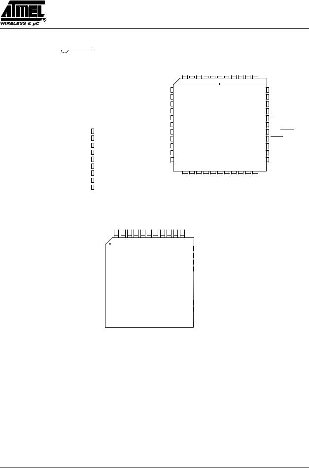
6. Pin Configuration
P1.0 / T2 |
|
1 |
|
|
40 |
|
|
VCC |
|
|
|
P1.4 |
P1.3/TxD1 |
P1.2/RxD1 |
|
P1.1/T2EX |
P1.0/T2 |
VSS1/NIC* |
VCC P0.0/AD0 |
P0.1/AD1 |
P0.2/AD2 |
P0.3/AD3 |
|||||||
|
|
|
|
|
|
|
|
|
|||||||||||||||||||||
P1.1 / T2EX |
|
2 |
|
|
39 |
|
|
P0.0 |
/ A0 |
|
|
|
|
|
|
|
|
|
|
|
|
|
|
||||||
|
|
|
|
|
|
|
|
|
|
|
|
|
|
|
|
|
|
|
|||||||||||
P1.2/RxD_1 |
|
3 |
|
|
38 |
|
|
P0.1 |
/ A1 |
|
|
|
|
|
|
|
|
|
|
|
|
|
|
||||||
|
|
|
|
|
|
|
|
|
|
|
|
|
|
|
|
|
|
|
|||||||||||
P1.3/TxD_1 |
|
4 |
|
|
37 |
|
P0.2 / A2 |
|
|
|
|
|
|
|
|
|
1 |
|
|
|
|
||||||||
|
|
|
|
|
|
|
|
|
|
|
|
|
|
|
|
|
|||||||||||||
|
|
P1.4 |
|
5 |
|
|
36 |
|
|
P0.3 / A3 |
|
|
6 |
5 |
4 |
3 |
2 |
44 43 42 41 40 |
|||||||||||
|
|
|
|
|
|
||||||||||||||||||||||||
|
|
P1.5 |
|
6 |
|
|
35 |
|
|
P0.4 |
/ A4 |
|
P1.5 |
7 |
|
|
|
|
|
|
|
|
|
|
39 |
||||
|
|
|
|
|
|
|
|
|
|
|
|
|
|
|
|||||||||||||||
P1.6/RxD_1 |
|
7 |
|
|
34 |
|
|
P0.5 |
/ A5 |
P1.6/RxD_1 |
8 |
|
|
|
|
|
|
|
|
|
|
38 |
|||||||
|
|
|
|
|
|
|
|
|
|
|
|
|
|
||||||||||||||||
P1.7/TxD_1 |
|
8 |
|
|
33 |
|
|
P0.6 |
/ A6 |
P1.7/TxD_1 |
9 |
|
|
|
|
|
|
|
|
|
|
37 |
|||||||
|
|
|
|
|
|
|
|
|
|
|
|
|
|
||||||||||||||||
RST |
|
9 |
|
|
32 |
|
|
P0.7 |
/ A7 |
|
RST |
10 |
|
|
|
|
|
|
|
|
|
|
36 |
||||||
|
|
|
|
|
|
|
|
|
|
|
|
|
|
|
|||||||||||||||
|
|
|
|
|
|
|
|
|
|
|
|
P3.0/RxD_0 |
|
|
|
|
|
|
|
|
|
|
|
|
|||||
P3.0/RxD_0 |
|
10 |
PDIL/ |
31 |
|
|
EA/VPP |
11 |
|
|
PLCC/CQPJ 44 |
|
|
35 |
|||||||||||||||
|
|
|
|
|
|
||||||||||||||||||||||||
|
|
|
|
|
|
|
|
|
|
|
|
|
|
RxD_1 |
12 |
|
|
|
|
|
|||||||||
P3.1/TxD_0 |
|
11 |
30 |
|
|
ALE/PROG |
|
|
|
|
34 |
||||||||||||||||||
|
|
|
|
|
|
|
|||||||||||||||||||||||
|
|
|
|
|
|
|
|
|
|||||||||||||||||||||
|
|
|
|
|
|
|
|
|
|
|
|
|
|
P3.1/TxD_0 |
13 |
|
|
|
|
|
|
|
|
|
|
|
|||
P3.2/INT0 |
|
|
12 CDIL40 |
29 |
|
|
PSEN |
|
|
|
|
|
|
|
|
|
|
33 |
|||||||||||
|
|
|
|
|
|
|
|
|
|
|
|
P2.7 |
/ A15 |
|
|
|
|
|
|
|
|
|
|
|
|
|
|
||
P3.3/INT1 |
|
|
13 |
|
|
28 |
|
|
P3.2/INT0 |
14 |
|
|
|
|
|
|
|
|
|
|
32 |
||||||||
|
|
|
|
|
|
|
|
|
|
|
|
|
|||||||||||||||||
|
|
|
|
|
|
|
|
|
|
|
|
P2.6 |
/ A14 |
|
|
|
|
|
|
|
|
|
|
|
|
|
|
||
P3.4/T0 |
|
14 |
|
|
27 |
P3.3/INT1 |
15 |
|
|
|
|
|
|
|
|
|
|
31 |
|||||||||||
|
|
|
|
|
|
|
|
|
|
|
|
|
|||||||||||||||||
|
|
|
|
|
P2.5 |
/ A13 |
|
|
|
|
|
|
|
|
|
|
|||||||||||||
P3.5/T1 |
|
15 |
|
|
26 |
|
|
P3.4/T0 |
16 |
|
|
|
|
|
|
|
|
|
|
30 |
|||||||||
|
|
|
|
|
|
|
|
|
|
|
|
|
|
|
|
|
|
|
|||||||||||
|
|
|
|
|
|
|
|
|
|
P2.4 |
/ A12 |
P3.5/T1 |
|
|
|
|
|
|
|
|
|
|
|
|
|||||
P3.6/WR |
|
16 |
|
|
25 |
|
17 |
|
|
|
|
|
|
|
|
|
|
29 |
|||||||||||
|
|
|
|
|
|
|
|
|
|
|
|
|
|
||||||||||||||||
|
|
|
|
|
|
17 |
|
|
24 |
|
|
P2.3 |
/ A11 |
|
|
|
|
|
|
|
|
|
|
|
|
|
|
||
P3.7/RD |
|
|
|
|
|
P2.2 |
/ A10 |
|
|
18 19 20 21 22 23 24 25 26 27 28 |
|||||||||||||||||||
|
18 |
|
|
23 |
|
|
|
|
|||||||||||||||||||||
XTAL2 |
|
|
|
|
|
|
|
|
P3.6/WR |
P3.7/RD |
XTAL2 |
|
XTAL1 |
VSS |
NIC* |
P2.0/A8 P2.1/A9 |
P2.2/A10 |
P2.3/A11 |
P2.4/A12 |
||||||||||
XTAL1 |
|
19 |
|
|
22 |
|
|
P2.1 |
/ A9 |
|
|
|
|
|
|
|
|
|
|
|
|
|
|
||||||
|
|
|
|
|
|
|
|
|
|
|
|
|
|
|
|
||||||||||||||
|
|
VSS |
|
20 |
|
|
21 |
|
|
P2.0 |
/ A8 |
|
|
|
|
|
|
|
|
|
|
|
|
|
|
||||
|
|
|
|
|
|
|
|
|
|
|
|
|
|
|
|
|
|
|
|||||||||||
|
|
|
|
|
|
|
|
|
|
|
|
|
|
|
|
|
|
|
|
|
|
|
|
|
|
|
|
|
|
|
|
|
|
|
|
|
P1.4 |
P1.3/TxD_1 |
P1.2/RxD_1 |
|
P1.1/T2EX |
|
P1.0/T2 |
|
VSS1/NIC* VCC |
|
P0.0/AD0 |
|
P0.1/AD1 |
|
P0.2/AD2 |
|
P0.3/AD3 |
|
|
|
|
|
|
||||||
|
|
|
|
|
|
|
|
|
|
|
|
|
|
|
|
|
|
|
|
|
|
|
|
|
|
|
|
|
|
|
|
||||
|
|
|
|
|
|
|
|
|
|
|
|
|
|
|
|
|
|
|
|
|
|
|
|
|
|
|
|
|
|
|
|
|
|
|
|
|
|
|
|
44 43 42 |
41 |
40 |
39 38 |
37 |
36 |
35 |
34 |
|
|
|
|
|
|
|
|||||||||||||||||
|
|
P1.5 |
|
|
|
|
|
|
|
|
|
|
|
|
|
|
|
|
|
|
|
|
|
33 |
|
|
P0.4/AD4 |
||||||||
|
|
1 |
|
|
|
|
|
|
|
|
|
|
|
|
|
|
|
|
|
|
|
|
|
|
|||||||||||
P1.6/RxD_1 |
|
|
2 |
|
|
|
|
|
|
|
|
|
|
|
|
|
|
|
|
|
|
|
|
32 |
|
|
P0.5/AD5 |
||||||||
|
|
|
|
|
|
|
|
|
|
|
|
|
|
|
|
|
|
|
|
|
|
|
|
||||||||||||
P1.7/TxD_1 |
|
|
3 |
|
|
|
|
|
|
|
|
|
|
|
|
|
|
|
|
|
|
|
|
31 |
|
|
P0.6/AD6 |
||||||||
|
|
|
|
|
|
|
|
|
|
|
|
|
|
|
|
|
|
|
|
|
|
|
|
||||||||||||
|
|
RST |
|
|
4 |
|
|
|
|
|
|
|
|
|
|
|
|
|
|
|
|
|
|
|
|
30 |
|
|
P0.7/AD7 |
||||||
|
|
|
|
|
|
|
|
|
|
|
|
|
|
|
|
|
|
|
|
|
|
|
|
||||||||||||
P3.0/RxD_0 |
|
|
|
|
|
|
|
|
|
|
|
|
|
|
|
|
|
|
|
|
|
|
|
29 |
|
|
|
|
|
|
|||||
|
|
5 |
|
|
|
|
|
|
|
VQFP44 1.4 |
|
|
|
|
EA/VPP |
||||||||||||||||||||
RxD_1 |
|
|
6 |
|
|
|
|
|
|
|
|
|
28 |
|
|
TxD_1 |
|||||||||||||||||||
|
|
|
|
|
|
|
|
|
|
|
|
|
|||||||||||||||||||||||
P3.1/TxD_0 |
|
|
|
|
|
|
|
|
|
|
|
|
|
|
|
|
|
|
|
|
|
|
|
27 |
|
|
|
|
|||||||
|
|
7 |
|
|
|
|
|
|
|
|
|
|
|
|
|
|
|
|
|
|
|
|
|
|
ALE/PROG |
||||||||||
|
|
|
|
|
|
8 |
|
|
|
|
|
|
|
|
|
|
|
|
|
|
|
|
|
|
|
|
26 |
|
|
|
|
|
|||
P3.2/INT0 |
|
|
|
|
|
|
|
|
|
|
|
|
|
|
|
|
|
|
|
|
|
|
|
|
|
PSEN |
|
||||||||
|
|
|
|
|
|
|
|
|
|
|
|
|
|
|
|
|
|
|
|
|
|
|
|
|
|
|
25 |
|
|
P2.7/A15 |
|||||
P3.3/INT1 |
|
|
|
9 |
|
|
|
|
|
|
|
|
|
|
|
|
|
|
|
|
|
|
|
|
|
|
|||||||||
P3.4/T0 |
|
|
10 |
|
|
|
|
|
|
|
|
|
|
|
|
|
|
|
|
|
|
|
|
24 |
|
|
P2.6/A14 |
||||||||
|
|
|
|
|
|
|
|
|
|
|
|
|
|
|
|
|
|
|
|
|
|
|
|
||||||||||||
P3.5/T1 |
|
|
11 |
|
|
|
|
|
|
|
|
|
|
|
|
|
|
|
|
|
|
|
|
23 |
|
|
P2.5/A13 |
||||||||
|
|
|
|
|
|
|
|
|
|
|
|
|
|
|
|
|
|
|
|
|
|
|
|
||||||||||||
|
|
|
|
12 13 14 15 16 17 18 19 20 21 22 |
|
|
|
|
|
|
|||||||||||||||||||||||||
|
|
|
|
|
|
|
|
|
|
|
|
|
|
|
|
|
|
|
|
|
|
|
|
|
|
|
|
|
|
|
|
|
|
|
|
|
|
|
|
|
|
|
|
|
|
|
|
|
|
|
|
|
|
|
|
|
|
|
|
|
|
|
|
|
|
|
|
|
|
|
|
*NIC: No Internal Connection |
|
|
|
P3.6/WR |
|
P3.7/RD |
XTAL2 |
|
XTAL1 |
|
VSS |
|
NIC* P2.0/A8 |
|
P2.1/A9 |
|
P2.2/A10 |
|
P2.3/A11 |
|
P2.4/A12 |
|
|
|
|
|
|
||||||||
|
|
|
|
|
|
|
|
|
|
|
|
|
|
|
|
|
|||||||||||||||||||
|
|
|
|
|
|
|
|
|
|
|
|
|
|
|
|
|
|||||||||||||||||||
|
|
|
|
|
|
|
|
|
|
|
|
|
|
|
|
|
|
|
|
|
|
|
|
|
|
|
|
|
|
|
|
||||
s
P0.4/AD4
P0.5/AD5
P0.6/AD6
P0.7/AD7
EA/VPP
TxD_1
ALE/PROG
PSEN
P2.7/A15
P2.6/A14
P2.5/A13
See “Alternate function on Port 1” on page 32 for accurate RxD_1 and TxD_1 pin location, depending on AUXR register configuration.
Rev. D - 15 January, 2001 |
5 |

TS80C51U2
TS83C51U2
TS87C51U2
Table 3. Pin Description for 40/44 pin packages
MNEMONIC |
PIN NUMBER |
TYPE |
|
|
|
|
NAME AND FUNCTION |
||
DIL |
LCC |
VQFP 1.4 |
|
|
|
|
|||
|
|
|
|
|
|
|
|||
|
|
|
|
|
|
|
|
|
|
VSS |
20 |
22 |
16 |
I |
|
Ground: 0V reference |
|||
Vss1 |
|
1 |
39 |
I |
|
Optional Ground: Contact the Sales Office for ground connection. |
|||
|
|
|
|
|
|
|
|||
VCC |
40 |
44 |
38 |
I |
|
Power Supply: This is the power supply voltage for normal, idle and power- |
|||
|
down operation |
||||||||
P0.0-P0.7 |
39-32 |
43-36 |
37-30 |
I/O |
|
Port 0: Port 0 is an open-drain, bidirectional I/O port. Port 0 pins that have 1s |
|||
|
|
|
|
|
|
written to them float and can be used as high impedance inputs. Port 0 pins must |
|||
|
|
|
|
|
|
be polarized to Vcc or Vss in order to prevent any parasitic current consumption. |
|||
|
|
|
|
|
|
Port 0 is also the multiplexed low-order address and data bus during access to |
|||
|
|
|
|
|
|
external program and data memory. In this application, it uses strong internal |
|||
|
|
|
|
|
|
pull-up when emitting 1s. Port 0 also inputs the code bytes during EPROM |
|||
|
|
|
|
|
|
programming. External pull-ups are required during program verification during |
|||
|
|
|
|
|
|
which P0 outputs the code bytes. |
|||
|
|
|
|
|
|
|
|||
P1.0-P1.7 |
1-8 |
2-9 |
40-44 |
I/O |
|
Port 1: Port 1 is an 8-bit bidirectional I/O port with internal pull-ups. Port 1 |
|||
|
|
|
1-3 |
|
|
pins that have 1s written to them are pulled high by the internal pull-ups and |
|||
|
|
|
|
|
|
can be used as inputs. As inputs, Port 1 pins that are externally pulled low will |
|||
|
|
|
|
|
|
source current because of the internal pull-ups. Port 1 also receives the low-order |
|||
|
|
|
|
|
|
address byte during memory programming and verification. |
|||
|
|
|
|
|
|
Alternate functions for TSC8x54/58 Port 1 include: |
|||
|
1 |
2 |
40 |
I/O |
|
T2 (P1.0): Timer/Counter 2 external count input/Clockout |
|||
|
2 |
3 |
41 |
I |
|
T2EX (P1.1): Timer/Counter 2 Reload/Capture/Direction Control |
|||
|
|
|
|
|
|
Depending on values of (M1UA_1, M0UA_1) bits located into AUXR register, |
|||
|
|
|
|
|
|
the UART_1 pins are alternate functins of P1 with two possible locations. |
|||
|
|
|
|
|
|
First location: |
|||
|
3 |
4 |
42 |
I |
|
P1.2: RxD_1, serial input port for UART_1 |
|||
|
4 |
5 |
43 |
O |
|
P1.3: TxD_1, serial output port for UART_1 |
|||
|
|
|
|
|
|
Second location: |
|||
|
7 |
8 |
2 |
I |
|
P1.6: RxD_1, serial input port for UART_1 |
|||
|
8 |
9 |
3 |
O |
|
P1.7: TxD_1, serial output port for UART_1 |
|||
|
|
|
|
|
|
See “Alternate function on Port 1” on page 32 |
|||
|
|
|
|
|
|
|
|||
P2.0-P2.7 |
21-28 |
24-31 |
18-25 |
I/O |
|
Port 2: Port 2 is an 8-bit bidirectional I/O port with internal pull-ups. Port 2 |
|||
|
|
|
|
|
|
pins that have 1s written to them are pulled high by the internal pull-ups and |
|||
|
|
|
|
|
|
can be used as inputs. As inputs, Port 2 pins that are externally pulled low will |
|||
|
|
|
|
|
|
source current because of the internal pull-ups. Port 2 emits the high-order address |
|||
|
|
|
|
|
|
byte during fetches from external program memory and during accesses to external |
|||
|
|
|
|
|
|
data memory that use 16-bit addresses (MOVX @DPTR).In this application, it |
|||
|
|
|
|
|
|
uses strong internal pull-ups emitting 1s. During accesses to external data memory |
|||
|
|
|
|
|
|
that use 8-bit addresses (MOVX @Ri), port 2 emits the contents of the P2 SFR. |
|||
|
|
|
|
|
|
Some Port 2 pins receive the high order address bits during EPROM programming |
|||
|
|
|
|
|
|
and verification: P2.0 to P2.5 |
|||
|
|
|
|
|
|
|
|||
P3.0-P3.7 |
10-17 |
11, |
5, |
I/O |
|
Port 3: Port 3 is an 8-bit bidirectional I/O port with internal pull-ups. Port 3 |
|||
|
|
13-19 |
7-13 |
|
|
pins that have 1s written to them are pulled high by the internal pull-ups and |
|||
|
|
|
|
|
|
can be used as inputs. As inputs, Port 3 pins that are externally pulled low will |
|||
|
|
|
|
|
|
source current because of the internal pull-ups. Port 3 also serves the special |
|||
|
|
|
|
|
|
features of the 80C51 family, as listed below. |
|||
|
10 |
11 |
5 |
I |
|
RxD_0 (P3.0): Serial input port for UART_0 |
|||
|
11 |
13 |
7 |
O |
|
TxD_0 (P3.1): Serial output port for UART_0 |
|||
|
12 |
14 |
8 |
I |
|
|
|
|
(P3.2): External interrupt 0 |
|
|
INT0 |
|||||||
|
13 |
15 |
9 |
I |
|
|
|
|
(P3.3): External interrupt 1 |
|
|
INT1 |
|||||||
|
14 |
16 |
10 |
I |
|
T0 (P3.4): Timer 0 external input |
|||
|
15 |
17 |
11 |
I |
|
T1 (P3.5): Timer 1 external input |
|||
|
16 |
18 |
12 |
O |
|
|
|
(P3.6): External data memory write strobe |
|
|
|
WR |
|||||||
|
17 |
19 |
13 |
O |
|
|
(P3.7): External data memory read strobe |
||
|
|
RD |
|||||||
6 |
Rev. D - 15 January, 2001 |

TS80C51U2
TS83C51U2
TS87C51U2
Table 3. Pin Description for 40/44 pin packages
|
MNEMONIC |
PIN NUMBER |
TYPE |
|
|
|
|
NAME AND FUNCTION |
||||||||||||||||
|
DIL |
LCC |
VQFP 1.4 |
|
|
|
|
|||||||||||||||||
|
|
|
|
|
|
|
|
|
|
|
|
|
|
|
|
|
|
|
|
|
|
|||
|
|
|
|
|
|
|
|
|
|
|
|
|
|
|
|
|
|
|
|
|
|
|
|
|
|
Reset |
9 |
10 |
4 |
I |
Reset: A high on this pin for two machine cycles while the oscillator is running, |
||||||||||||||||||
|
|
|
|
|
|
|
|
|
|
resets the device. An internal diffused resistor to VSS permits a power-on reset |
||||||||||||||
|
|
|
|
|
|
|
|
|
|
using only an external capacitor to VCC. If the hardware watchdog reaches its |
||||||||||||||
|
|
|
|
|
|
|
|
|
|
time-out, the reset pin becomes an output during the time the internal reset is |
||||||||||||||
|
|
|
|
|
|
|
|
|
|
activated. |
||||||||||||||
|
|
|
|
|
|
|
|
|
|
|
|
|
|
|
|
|
|
|
|
|
|
|
|
|
|
|
|
|
|
|
30 |
33 |
27 |
O (I) |
Address Latch Enable/Program Pulse: Output pulse for latching the low byte |
||||||||||||||
|
ALE/PROG |
|
||||||||||||||||||||||
|
|
|
|
|
|
|
|
|
|
of the address during an access to external memory. In normal operation, ALE |
||||||||||||||
|
|
|
|
|
|
|
|
|
|
is emitted at a constant rate of 1/6 (1/3 in X2 mode) the oscillator frequency, |
||||||||||||||
|
|
|
|
|
|
|
|
|
|
and can be used for external timing or clocking. Note that one ALE pulse is |
||||||||||||||
|
|
|
|
|
|
|
|
|
|
skipped during each access to external data memory. This pin is also the program |
||||||||||||||
|
|
|
|
|
|
|
|
|
|
pulse input |
|
|
|
during EPROM programming. ALE can be disabled by |
||||||||||
|
|
|
|
|
|
|
|
|
|
(PROG) |
||||||||||||||
|
|
|
|
|
|
|
|
|
|
setting SFR’s AUXR.0 bit. With this bit set, ALE will be inactive during internal |
||||||||||||||
|
|
|
|
|
|
|
|
|
|
fetches. |
||||||||||||||
|
|
|
|
|
|
|
|
|
||||||||||||||||
|
|
|
|
|
29 |
32 |
26 |
O |
Program Store ENable: The read strobe to external program memory. When |
|||||||||||||||
|
PSEN |
|||||||||||||||||||||||
|
|
|
|
|
|
|
|
|
|
executing code from the external program memory, |
|
is activated twice each |
||||||||||||
|
|
|
|
|
|
|
|
|
|
PSEN |
||||||||||||||
|
|
|
|
|
|
|
|
|
|
machine cycle, except that two |
PSEN |
activations are skipped during each access |
||||||||||||
|
|
|
|
|
|
|
|
|
|
to external data memory. |
|
is not activated during fetches from internal |
||||||||||||
|
|
|
|
|
|
|
|
|
|
PSEN |
||||||||||||||
|
|
|
|
|
|
|
|
|
|
program memory. |
||||||||||||||
|
|
|
|
|
|
|
|
|
||||||||||||||||
|
|
|
|
|
|
31 |
35 |
29 |
I |
External Access Enable/Programming Supply Voltage: |
|
must be externally |
||||||||||||
|
EA/VPP |
EA |
||||||||||||||||||||||
|
|
|
|
|
|
|
|
|
|
held low to enable the device to fetch code from external program memory |
||||||||||||||
|
|
|
|
|
|
|
|
|
|
locations 0000H and 3FFFH (RB) or 7FFFH (RC), or FFFFH (RD). If EA is |
||||||||||||||
|
|
|
|
|
|
|
|
|
|
held high, the device executes from internal program memory unless the program |
||||||||||||||
|
|
|
|
|
|
|
|
|
|
counter contains an address greater than 3FFFH (RB) or 7FFFH (RC) |
|
must |
||||||||||||
|
|
|
|
|
|
|
|
|
|
EA |
||||||||||||||
|
|
|
|
|
|
|
|
|
|
be held low for ROMless devices. This pin also receives the 12.75V programming |
||||||||||||||
|
|
|
|
|
|
|
|
|
|
supply voltage (VPP) during EPROM programming. If security level 1 is |
||||||||||||||
|
|
|
|
|
|
|
|
|
|
programmed, |
EA |
will be internally latched on Reset. |
||||||||||||
|
XTAL1 |
19 |
21 |
15 |
I |
Crystal 1: Input to the inverting oscillator amplifier and input to the internal |
||||||||||||||||||
|
|
|
|
|
|
|
|
|
|
clock generator circuits. |
||||||||||||||
|
|
|
|
|
|
|
||||||||||||||||||
|
XTAL2 |
18 |
20 |
14 |
O |
Crystal 2: Output from the inverting oscillator amplifier |
||||||||||||||||||
|
|
|
|
|
|
|
||||||||||||||||||
|
RxD_1 |
- |
12 |
6 |
I |
Serial Input for UART_1. For 44-pin package only. |
||||||||||||||||||
|
|
|
|
|
|
|
|
|
|
|
||||||||||||||
|
TxD_1 |
- |
34 |
28 |
O |
Serial Ouput for UART_1. This pin is pulled up by a 100K resistor when not |
||||||||||||||||||
|
selected. For 44-pin package only. |
|||||||||||||||||||||||
|
|
|
|
|
|
|
|
|
|
|||||||||||||||
|
|
|
|
|
|
|
|
|
|
|
|
|
|
|
|
|
|
|
|
|
|
|
|
|
Rev. D - 15 January, 2001 |
7 |

TS87C51U2
7. TS80C51U2 Enhanced Features
In comparison to the original 80C52, the TS80C51U2 implements some new features, which are:
∙The X2 option.
∙The second full duplex enhanced UART.
∙The Baud Rate generator.
∙The Dual Data Pointer.
∙The Watchdog.
∙The 4 level interrupt priority system.
∙The power-off flag.
∙The ONCE mode.
∙The ALE disabling.
∙Some enhanced features are also located in the UARTs and the timer 2.
7.1X2 Feature
The TS80C51U2 core needs only 6 clock periods per machine cycle. This feature called ”X2” provides the following advantages:
●Divide frequency crystals by 2 (cheaper crystals) while keeping same CPU power.
●Save power consumption while keeping same CPU power (oscillator power saving).
●Save power consumption by dividing dynamically operating frequency by 2 in operating and idle modes.
●Increase CPU power by 2 while keeping same crystal frequency.
In order to keep the original C51 compatibility, a divider by 2 is inserted between the XTAL1 signal and the main clock input of the core (phase generator). This divider may be disabled by software.
7.1.1 Description
The clock for the whole circuit and peripheral is first divided by two before being used by the CPU core and peripherals. This allows any cyclic ratio to be accepted on XTAL1 input. In X2 mode, as this divider is bypassed,
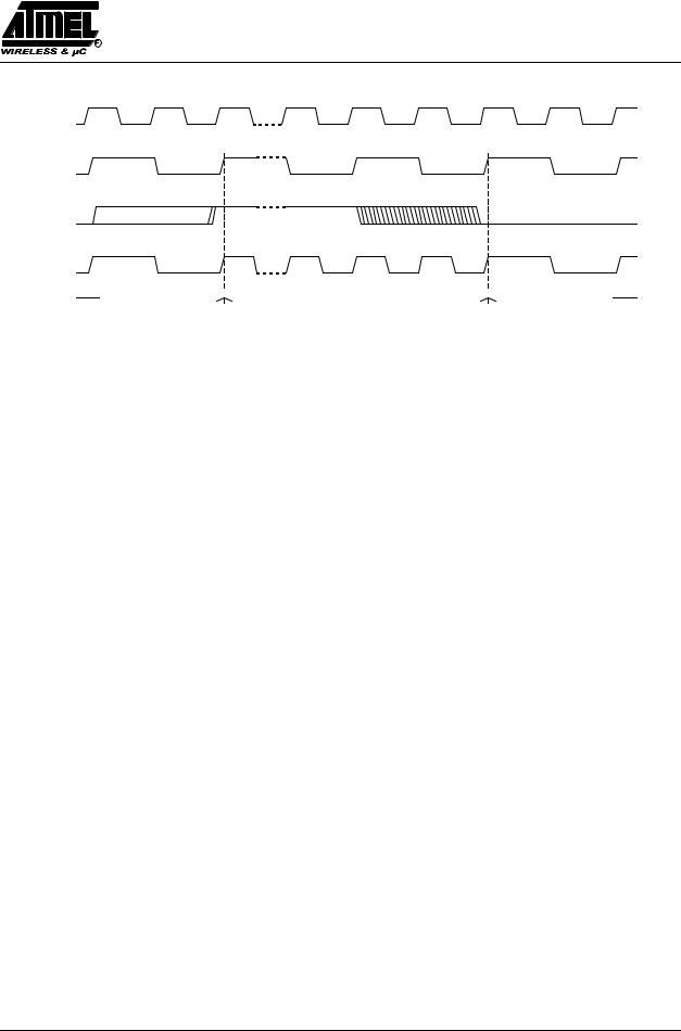
the signals on XTAL1 must have a cyclic ratio between 40 to 60%. Figure 1. shows the clock generation block diagram. X2 bit is validated on XTAL1÷2 rising edge to avoid glitches when switching from X2 to STD mode.
Figure 2. shows the mode switching waveforms.
|
|
|
|
|
|
XTAL1:2 |
|
||
XTAL1 |
|
|
|
|
2 |
0 |
|
state machine: 6 clock cycles. |
|
|
|
||||||||
|
FXTAL |
|
|
|
1 |
|
CPU control |
||
|
|
|
|
|
|
||||
FOSC
X2
CKCON reg
Figure 1. Clock Generation Diagram
8 |
Rev. D - 06 december, 2000 |
TS87C51U2
XTAL1
XTAL1:2
X2 bit
CPU clock
STD Mode X2 Mode
  STD Mode
Figure 2. Mode Switching Waveforms
The X2 bit in the CKCON register (See Table 4.) allows to switch from 12 clock cycles per instruction to 6 clock cycles and vice versa. At reset, the standard speed is activated (STD mode). Setting this bit activates the X2 feature (X2 mode).
CAUTION
In order to prevent any incorrect operation while operating in X2 mode, user must be aware that all peripherals using clock frequency as time reference (UARTs, timers) will have their time reference divided by two. For example a free running timer generating an interrupt every 20 ms will then generate an interrupt every 10 ms. UART with 4800 baud rate will have 9600 baud rate.
Rev. D - 06 december, 2000 |
9 |

TS87C51U2
Table 4. CKCON Register
CKCON - Clock Control Register (8Fh)
7 |
|
6 |
|
5 |
4 |
3 |
|
2 |
|
1 |
0 |
|
|
|
|
|
|
|
|
|
|
|
|
- |
|
- |
|
- |
- |
- |
|
- |
|
- |
X2 |
|
|
|
|
|
|
|
|
|
|
|
|
|
|
|
|
|
|
|
|
|
|
|
|
Bit |
|
Bit |
|
|
|
Description |
|
|
|
|
|
Number |
Mnemonic |
|
|
|
|
|
|
|
|||
|
|
|
|
|
|
|
|
|
|||
|
|
|
|
|
|
|
|
|
|
|
|
7 |
- |
Reserved |
|
|
|
|
|
|
|
||
|
The value read from this bit is indeterminate. Do not set this bit. |
|
|
||||||||
|
|
|
|
|
|
||||||
|
|
|
|
|
|
|
|
|
|
|
|
6 |
- |
Reserved |
|
|
|
|
|
|
|
||
|
The value read from this bit is indeterminate. Do not set this bit. |
|
|
||||||||
|
|
|
|
|
|
||||||
|
|
|
|
|
|
|
|
|
|
|
|
5 |
- |
Reserved |
|
|
|
|
|
|
|
||
|
The value read from this bit is indeterminate. Do not set this bit. |
|
|
||||||||
|
|
|
|
|
|
||||||
|
|
|
|
|
|
|
|
|
|
|
|
4 |
- |
Reserved |
|
|
|
|
|
|
|
||
|
The value read from this bit is indeterminate. Do not set this bit. |
|
|
||||||||
|
|
|
|
|
|
||||||
|
|
|
|
|
|
|
|
|
|
|
|
3 |
- |
Reserved |
|
|
|
|
|
|
|
||
|
The value read from this bit is indeterminate. Do not set this bit. |
|
|
||||||||
|
|
|
|
|
|
||||||
|
|
|
|
|
|
|
|
|
|
|
|
2 |
- |
Reserved |
|
|
|
|
|
|
|
||
|
The value read from this bit is indeterminate. Do not set this bit. |
|
|
||||||||
|
|
|
|
|
|
||||||
|
|
|
|
|
|
|
|
|
|
|
|
1 |
- |
Reserved |
|
|
|
|
|
|
|
||
|
The value read from this bit is indeterminate. Do not set this bit. |
|
|
||||||||
|
|
|
|
|
|
||||||
|
|
|
|
|
|
|
|
|
|
|
|
|
|
|
CPU and peripheral clock bit |
|
|
|
|
|
|
||
0 |
|
X2 |
|
Clear to select 12 clock periods per machine cycle (STD mode, FOSC=FXTAL/2). |
|
|
|||||
|
|
|
|
Set to select 6 clock periods per machine cycle (X2 mode, FOSC=FXTAL). |
|
|
|||||
|
|
|
|
|
|
|
|
|
|
|
|
Reset Value = XXXX XXX0b
Not bit addressable
For further details on the X2 feature, please refer to ANM072 available on the web (http://www.atmel-wm.com)
10 |
Rev. D - 06 december, 2000 |
TS80C51U2
TS83C51U2
TS87C51U2
7.2 Dual Data Pointer Register Ddptr
The additional data pointer can be used to speed up code execution and reduce code size in a number of ways.
The dual DPTR structure is a way by which the chip will specify the address of an external data memory location. There are two 16-bit DPTR registers that address the external memory, and a single bit called DPS = AUXR1/bit0 (See Table 5.) that allows the program code to switch between them (Refer to Figure 3).
External Data Memory
7 |
|
0 |
|
|
|
DPS |
DPTR1 |
|
|
|
|
|
AUXR1(A2H) |
|
DPTR0 |
|
|
|
|
|
|
|
DPH(83H) DPL(82H) |
Figure 3. Use of Dual Pointer
Rev. D - 15 January, 2001 |
11 |

TS80C51U2
TS83C51U2
TS87C51U2
Table 5. AUXR1: Auxiliary Register 1
7 |
|
6 |
|
5 |
|
4 |
3 |
|
2 |
1 |
0 |
|
|
|
|
|
|
|
|
|
|
|
|
- |
|
- |
|
- |
|
- |
- |
|
- |
- |
DPS |
|
|
|
|
|
|
|
|
|
|
|
|
|
|
|
|
|
|
|
|
|
|
|
|
Bit |
|
Bit |
|
|
|
|
Description |
|
|
|
|
Number |
Mnemonic |
|
|
|
|
|
|
|
|||
|
|
|
|
|
|
|
|
|
|||
|
|
|
|
|
|
|
|
|
|
|
|
7 |
- |
Reserved |
|
|
|
|
|
|
|||
|
The value read from this bit is indeterminate. Do not set this bit. |
|
|
||||||||
|
|
|
|
|
|
||||||
|
|
|
|
|
|
|
|
|
|
|
|
6 |
- |
Reserved |
|
|
|
|
|
|
|||
|
The value read from this bit is indeterminate. Do not set this bit. |
|
|
||||||||
|
|
|
|
|
|
||||||
|
|
|
|
|
|
|
|
|
|
|
|
5 |
- |
Reserved |
|
|
|
|
|
|
|||
|
The value read from this bit is indeterminate. Do not set this bit. |
|
|
||||||||
|
|
|
|
|
|
||||||
|
|
|
|
|
|
|
|
|
|
|
|
4 |
- |
Reserved |
|
|
|
|
|
|
|||
|
The value read from this bit is indeterminate. Do not set this bit. |
|
|
||||||||
|
|
|
|
|
|
||||||
|
|
|
|
|
|
|
|
|
|
|
|
3 |
- |
Reserved |
|
|
|
|
|
|
|||
|
The value read from this bit is indeterminate. Do not set this bit. |
|
|
||||||||
|
|
|
|
|
|
||||||
|
|
|
|
|
|
|
|
|
|
|
|
2 |
- |
Reserved |
|
|
|
|
|
|
|||
|
The value read from this bit is indeterminate. Do not set this bit. |
|
|
||||||||
|
|
|
|
|
|
||||||
|
|
|
|
|
|
|
|
|
|
|
|
1 |
- |
Reserved |
|
|
|
|
|
|
|||
|
The value read from this bit is indeterminate. Do not set this bit. |
|
|
||||||||
|
|
|
|
|
|
||||||
|
|
|
|
|
|
|
|
|
|
|
|
0 |
|
DPS |
Data Pointer Selection |
|
|
|
|
|
|
||
|
|
Clear to select DPTR0. |
|
|
|
|
|
|
|||
|
|
|
|
Set to select DPTR1. |
|
|
|
|
|
|
|
|
|
|
|
|
|
|
|
|
|
|
|
Reset Value = XXXX XXX0 Not bit addressable
User software should not write 1s to reserved bits. These bits may be used in future 8051 family products to invoke new feature. In that case, the reset value of the new bit will be 0, and its active value will be 1. The value read from a reserved bit is indeterminate.
Application
Software can take advantage of the additional data pointers to both increase speed and reduce code size, for example, block operations (copy, compare, search ...) are well served by using one data pointer as a ’source’ pointer and the other one as a "destination" pointer.
12 |
Rev. D - 15 January, 2001 |

TS80C51U2
TS83C51U2
TS87C51U2
ASSEMBLY LANGUAGE
;Block move using dual data pointers
;Destroys DPTR0, DPTR1, A and PSW
;note: DPS exits opposite of entry state
;unless an extra INC AUXR1 is added
00A2 AUXR1 EQU 0A2H
0000 |
909000MOV |
DPTR,#SOURCE |
; address of SOURCE |
|
0003 |
05A2 |
INC |
AUXR1 |
; switch data pointers |
0005 |
90A000 MOV DPTR,#DEST |
; address of DEST |
||
0008 |
|
LOOP: |
|
|
0008 |
05A2 |
INC |
AUXR1 |
; switch data pointers |
000A E0 |
MOVX A,@DPTR |
; get a byte from SOURCE |
||
000B A3 |
INC |
DPTR |
; increment SOURCE address |
|
000C 05A2 |
INC |
AUXR1 |
; switch data pointers |
|
000E F0 |
MOVX @DPTR,A |
; write the byte to DEST |
||
000F A3 |
INC |
DPTR |
; increment DEST address |
|
0010 |
70F6 |
JNZ |
LOOP |
; check for 0 terminator |
0012 |
05A2 |
INC |
AUXR1 |
; (optional) restore DPS |
INC is a short (2 bytes) and fast (12 clocks) way to manipulate the DPS bit in the AUXR1 SFR. However, note that the INC instruction does not directly force the DPS bit to a particular state, but simply toggles it. In simple routines, such as the block move example, only the fact that DPS is toggled in the proper sequence matters, not its actual value. In other words, the block move routine works the same whether DPS is '0' or '1' on entry. Observe that without the last instruction (INC AUXR1), the routine will exit with DPS in the opposite state.
Rev. D - 15 January, 2001 |
13 |

TS80C51U2
TS83C51U2
TS87C51U2
7.3 Timer 2
The timer 2 in the TS80C51U2 is compatible with the timer 2 in the 80C52.
It is a 16-bit timer/counter: the count is maintained by two eight-bit timer registers, TH2 and TL2, connected in cascade. It is controlled by T2CON register (See Table 6) and T2MOD register (See Table 7). Timer 2 operation is similar to Timer 0 and Timer 1. C/T2 selects FOSC/12 (timer operation) or external pin T2 (counter operation) as the timer clock input. Setting TR2 allows TL2 to be incremented by the selected input.
Timer 2 has 3 operating modes: capture, autoreload and Baud Rate Generator. These modes are selected by the combination of RCLK, TCLK and CP/RL2 (T2CON), as described in the Atmel Wireless & Microcontrollers 8- bit Microcontroller Hardware description.
Refer to the Atmel Wireless & Microcontrollers 8-bit Microcontroller Hardware description for the description of Capture and Baud Rate Generator Modes.
In TS80C51U2 Timer 2 includes the following enhancements:
●Auto-reload mode with up or down counter
●Programmable clock-output
7.3.1 Auto-Reload Mode
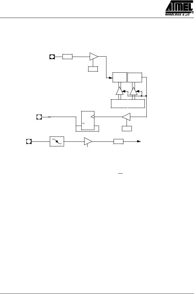
The auto-reload mode configures timer 2 as a 16-bit timer or event counter with automatic reload. If DCEN bit in T2MOD is cleared, timer 2 behaves as in 80C52 (refer to the Atmel Wireless & Microcontrollers 8-bit Microcontroller Hardware description). If DCEN bit is set, timer 2 acts as an Up/down timer/counter as shown in Figure 4. In this mode the T2EX pin controls the direction of count.
When T2EX is high, timer 2 counts up. Timer overflow occurs at FFFFh which sets the TF2 flag and generates an interrupt request. The overflow also causes the 16-bit value in RCAP2H and RCAP2L registers to be loaded into the timer registers TH2 and TL2.
When T2EX is low, timer 2 counts down. Timer underflow occurs when the count in the timer registers TH2 and TL2 equals the value stored in RCAP2H and RCAP2L registers. The underflow sets TF2 flag and reloads FFFFh into the timer registers.
The EXF2 bit toggles when timer 2 overflows or underflows according to the the direction of the count. EXF2 does not generate any interrupt. This bit can be used to provide 17-bit resolution.
14 |
Rev. D - 15 January, 2001 |
TS80C51U2
TS83C51U2
TS87C51U2
|
|
|
|
(:6 in X2 mode) |
|
||
XTAL1 |
|
|
|
|
:12 |
|
0 |
|
|
|
|||||
|
|
FOSC |
|
|
|||
FXTAL |
|
|
|
|
1 |
||
|
|
|
|
||||
T2 

C/T2 TR2
T2CONreg T2CONreg
(DOWN COUNTING RELOAD VALUE) |
T2EX: |
|
||
FFh |
FFh |
if DCEN=1, 1=UP |
||
(8-bit) |
(8-bit) |
if DCEN=1, 0=DOWN |
||
|
|
if DCEN = 0, up counting |
||
|
|
TOGGLE |
T2CONreg |
|
|
|
|
EXF2 |
|
TL2 |
TH2 |
TF2 |
TIMER 2 |
|
(8-bit) |
(8-bit) |
INTERRUPT |
||
T2CONreg |
||||
|
|
|
||
RCAP2L |
|
RCAP2H |
(8-bit) |
|
(8-bit) |
(UP COUNTING RELOAD VALUE)
Figure 4. Auto-Reload Mode Up/Down Counter (DCEN = 1)
7.3.2 Programmable Clock-Output
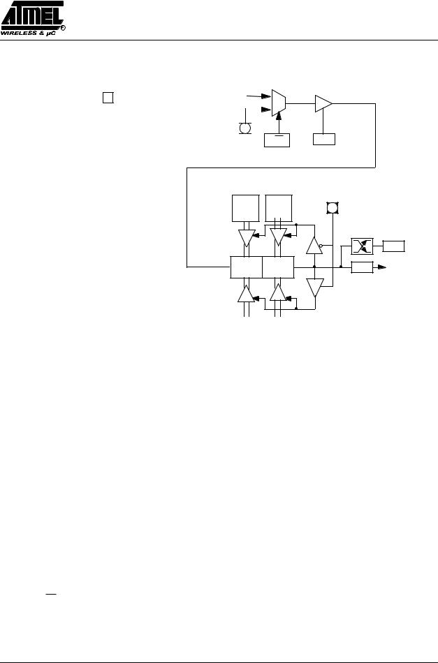
In the clock-out mode, timer 2 operates as a 50%-duty-cycle, programmable clock generator (See Figure 5) . The input clock increments TL2 at frequency FOSC/2. The timer repeatedly counts to overflow from a loaded value. At overflow, the contents of RCAP2H and RCAP2L registers are loaded into TH2 and TL2. In this mode, timer 2 overflows do not generate interrupts. The formula gives the clock-out frequency as a function of the system oscillator frequency and the value in the RCAP2H and RCAP2L registers:
Fosc
Clock –OutFrequency = --------------------------------------------------------------------------------------
4 ´ (65536 –RCAP2H ¤ RCAP2L)
For a 16 MHz system clock, timer 2 has a programmable frequency range of 61 Hz (FOSC/216) to 4 MHz (FOSC/4). The generated clock signal is brought out to T2 pin (P1.0).
Timer 2 is programmed for the clock-out mode as follows:
●Set T2OE bit in T2MOD register.
●Clear C/T2 bit in T2CON register.
●Determine the 16-bit reload value from the formula and enter it in RCAP2H/RCAP2L registers.
●Enter a 16-bit initial value in timer registers TH2/TL2. It can be the same as the reload value or a different one depending on the application.
Rev. D - 15 January, 2001 |
15 |
TS80C51U2
TS83C51U2
TS87C51U2
● To start the timer, set TR2 run control bit in T2CON register.
It is possible to use timer 2 as a baud rate generator and a clock generator simultaneously. For this configuration, the baud rates and clock frequencies are not independent since both functions use the values in the RCAP2H and RCAP2L registers.
XTAL1 :2
(:1 in X2 mode)
TR2
T2CON reg TL2 TH2 (8-bit) (8-bit)
OVERFLOW
RCAP2L 
 RCAP2H (8-bit) (8-bit)
Toggle
T2
Q D
T2OE
T2MOD reg
T2EX |
EXF2 |
TIMER 2 |
|
INTERRUPT |
|||
|
|
T2CON reg
EXEN2
T2CON reg
Figure 5. Clock-Out Mode C/T2 = 0
16 |
Rev. D - 15 January, 2001 |

TS80C51U2
TS83C51U2
TS87C51U2
Table 6. T2CON Register
T2CON - Timer 2 Control Register (C8h)
7 |
|
6 |
|
5 |
|
4 |
3 |
|
2 |
|
1 |
|
0 |
|
|
|
|
|
|
|
|
|
|
|
|
|
|
TF2 |
|
EXF2 |
|
RCLK |
|
TCLK |
EXEN2 |
|
TR2 |
|
C/T2# |
|
CP/RL2# |
|
|
|
|
|
|
|
|
|
|
|
|
|
|
|
|
|
|
|
|
|
|
|
|
|
|
|
|
Bit |
|
Bit |
|
|
|
|
Description |
|
|
|
|
|
|
Number |
Mnemonic |
|
|
|
|
|
|
|
|
|
|||
|
|
|
|
|
|
|
|
|
|
|
|||
|
|
|
|
|
|
|
|
|
|
|
|
|
|
|
|
|
Timer 2 overflow Flag |
|
|
|
|
|
|
|
|
||
7 |
|
TF2 |
|
Must be cleared by software. |
|
|
|
|
|
|
|
||
|
|
|
|
Set by hardware on timer 2 overflow, if RCLK = 0 and TCLK = 0. |
|
|
|
||||||
|
|
|
|
|
|
|
|
|
|
|
|
|
|
|
|
|
Timer 2 External Flag |
|
|
|
|
|
|
|
|
||
6 |
|
EXF2 |
|
Set when a capture or a reload is caused by a negative transition on T2EX pin if EXEN2=1. |
|
||||||||
|
|
When set, causes the CPU to vector to timer 2 interrupt routine when timer 2 interrupt is enabled. |
|||||||||||
|
|
|
|
||||||||||
|
|
|
|
Must be cleared by software. EXF2 doesn’t cause an interrupt in Up/down counter mode (DCEN = 1) |
|||||||||
|
|
|
|
|
|
|
|
|
|
|
|
|
|
|
|
|
Receive Clock bit for UART_0 |
|
|
|
|
|
|
|
|||
5 |
|
RCLK_0 |
|
Clear to use timer 1 overflow as receive clock for serial port in mode 1 or 3. |
|
|
|
||||||
|
|
|
|
Set to use timer 2 overflow as receive clock for serial port in mode 1 or 3. |
|
|
|
||||||
|
|
|
|
|
|
|
|
|
|
|
|
|
|
|
|
|
Transmit Clock bit for UART_0 |
|
|
|
|
|
|
|
|||
4 |
|
TCLK_0 |
|
Clear to use timer 1 overflow as transmit clock for serial port in mode 1 or 3. |
|
|
|
||||||
|
|
|
|
Set to use timer 2 overflow as transmit clock for serial port in mode 1 or 3. |
|
|
|
||||||
|
|
|
|
|
|
|
|
|
|
|
|
|
|
|
|
|
Timer 2 External Enable bit |
|
|
|
|
|
|
|
|||
3 |
|
EXEN2 |
|
Clear to ignore events on T2EX pin for timer 2 operation. |
|
|
|
|
|
||||
|
|
Set to cause a capture or reload when a negative transition on T2EX pin is detected, if timer 2 is not used to |
|||||||||||
|
|
|
|
||||||||||
|
|
|
clock the serial port. |
|
|
|
|
|
|
|
|
||
|
|
|
|
|
|
|
|
|
|
|
|
|
|
|
|
|
Timer 2 Run control bit |
|
|
|
|
|
|
|
|
||
2 |
|
TR2 |
|
Clear to turn off timer 2. |
|
|
|
|
|
|
|
||
|
|
|
|
Set to turn on timer 2. |
|
|
|
|
|
|
|
|
|
|
|
|
|
|
|
|
|
|
|
|
|
|
|
|
|
|
Timer/Counter 2 select bit |
|
|
|
|
|
|
|
|||
1 |
|
C/T2# |
|
Clear for timer operation (input from internal clock system: FOSC). |
|
|
|
||||||
|
|
|
|
Set for counter operation (input from T2 input pin, falling edge trigger). Must be 0 for clock out mode. |
|||||||||
|
|
|
|
|
|
|
|
|
|
|
|
|
|
|
|
|
Timer 2 Capture/Reload bit |
|
|
|
|
|
|
|
|||
0 |
|
CP/RL2# |
|
If RCLK=1 or TCLK=1, CP/RL2# is ignored and timer is forced to auto-reload on timer 2 overflow. |
|||||||||
|
|
Clear to auto-reload on timer 2 overflows or negative transitions on T2EX pin if EXEN2=1. |
|
||||||||||
|
|
|
|
|
|||||||||
|
|
|
|
Set to capture on negative transitions on T2EX pin if EXEN2=1. |
|
|
|
||||||
|
|
|
|
|
|
|
|
|
|
|
|
|
|
Reset Value = 0000 0000b
Bit addressable
Rev. D - 15 January, 2001 |
17 |

TS80C51U2
TS83C51U2
TS87C51U2
Table 7. T2MOD Register
T2MOD - Timer 2 Mode Control Register (C9h)
7 |
|
6 |
|
5 |
|
4 |
|
3 |
|
2 |
1 |
0 |
|
|
|
|
|
|
|
|
|
|
|
|
|
- |
|
- |
|
- |
|
- |
|
- |
|
- |
T2OE |
DCEN |
|
|
|
|
|
|
|
|
|
|
|
|
|
|
|
|
|
|
|
|
|
|
|
|
|
|
Bit |
|
Bit |
|
|
|
|
|
Description |
|
|
|
|
Number |
Mnemonic |
|
|
|
|
|
|
|
|
|||
|
|
|
|
|
|
|
|
|
|
|||
|
|
|
|
|
|
|
|
|
|
|
|
|
7 |
- |
Reserved |
|
|
|
|
|
|
|
|||
|
The value read from this bit is indeterminate. Do not set this bit. |
|
|
|||||||||
|
|
|
|
|
|
|||||||
|
|
|
|
|
|
|
|
|
|
|
|
|
6 |
- |
Reserved |
|
|
|
|
|
|
|
|||
|
The value read from this bit is indeterminate. Do not set this bit. |
|
|
|||||||||
|
|
|
|
|
|
|||||||
|
|
|
|
|
|
|
|
|
|
|
|
|
5 |
- |
Reserved |
|
|
|
|
|
|
|
|||
|
The value read from this bit is indeterminate. Do not set this bit. |
|
|
|||||||||
|
|
|
|
|
|
|||||||
|
|
|
|
|
|
|
|
|
|
|
|
|
4 |
- |
Reserved |
|
|
|
|
|
|
|
|||
|
The value read from this bit is indeterminate. Do not set this bit. |
|
|
|||||||||
|
|
|
|
|
|
|||||||
|
|
|
|
|
|
|
|
|
|
|
|
|
3 |
- |
Reserved |
|
|
|
|
|
|
|
|||
|
The value read from this bit is indeterminate. Do not set this bit. |
|
|
|||||||||
|
|
|
|
|
|
|||||||
|
|
|
|
|
|
|
|
|
|
|
|
|
2 |
- |
Reserved |
|
|
|
|
|
|
|
|||
|
The value read from this bit is indeterminate. Do not set this bit. |
|
|
|||||||||
|
|
|
|
|
|
|||||||
|
|
|
|
|
|
|
|
|
|
|
|
|
|
|
|
Timer 2 Output Enable bit |
|
|
|
|
|
|
|
||
1 |
|
T2OE |
|
Clear to program P1.0/T2 as clock input or I/O port. |
|
|
|
|||||
|
|
|
|
Set to program P1.0/T2 as clock output. |
|
|
|
|
|
|||
|
|
|
|
|
|
|
|
|
|
|
|
|
|
|
|
Down Counter Enable bit |
|
|
|
|
|
|
|
||
0 |
|
DCEN |
|
Clear to disable timer 2 as up/down counter. |
|
|
|
|||||
|
|
|
|
Set to enable timer 2 as up/down counter. |
|
|
|
|
|
|||
|
|
|
|
|
|
|
|
|
|
|
|
|
Reset Value = XXXX XX00b
Not bit addressable
18 |
Rev. D - 15 January, 2001 |
TS80C51U2
TS83C51U2
TS87C51U2
7.4 TS80C51U2 Serial I/O Ports enhancements
The serial I/O ports in the TS80C51U2 are compatible with the serial I/O port in the 80C52.
They provide both synchronous and asynchronous communication modes. They operate as Universal Asynchronous Receiver and Transmitter (UART) in three full-duplex modes (Modes 1, 2 and 3). Asynchronous transmission and reception can occur simultaneously and at different baud rates
Serial I/O ports include the following enhancements:
●Framing error detection
●Automatic address recognition
As these improvements apply to both UART, most of the time in the following lines, there won’t be any reference to UART_0 or UART_1, but only to UART, generally speaking. Idem for the bits in registers.
7.4.1 Framing Error Detection
Framing bit error detection is provided for the three asynchronous modes (modes 1, 2 and 3). To enable the framing bit error detection feature, set SMOD0 bit in PCON register (See Figure 6).
SM0/FE |
|
SM1 |
SM2 |
|
REN |
TB8 |
RB8 |
TI |
RI |
SCON_0 for UART_0 (98h) |
|||
|
|
|
|
|
|
|
|
|
|
|
|
|
(SCON_1 for UART_1 (C0h)) |
|
|
|
|
|
|
|
|
|
|
|
|
|
|
|
|
|
|
|
|
|
|
|
|||||
|
|
|
|
|
|
|
Set FE bit if stop bit is 0 (framing error) |
(SMOD0_0 = 1 for UART_0) |
|||||
|
|
|
|
|
|
||||||||
|
|
|
|
|
|
|
|
|
|
|
|
|
|
|
|
|
|
|
|
|
|
|
|
|
|
|
|
 SM0 to UART mode control (SMOD0_0 = 0 for UART_0)
SMOD1_0 |
SMOD0_0 |
- |
|
POF |
GF1 |
GF0 |
PD |
IDL |
PCON for UART_0 (87h) |
||
|
|
|
|
|
|
|
|
|
|
|
(SMOD bits for UART_1 are |
|
|
|
|
|
To UART framing error control |
|
|
||||
|
|
|
|
|
|
|
located in BDRCON_1) |
||||
|
|
|
|
|
|
|
|||||
|
|
|
|
|
|
|
|
|
|
|
|
Figure 6. Framing Error Block Diagram
When this feature is enabled, the receiver checks each incoming data frame for a valid stop bit. An invalid stop bit may result from noise on the serial lines or from simultaneous transmission by two CPUs. If a valid stop bit is not found, the Framing Error bit (FE) in SCON register (See Table 8.) bit is set.
Rev. D - 15 January, 2001 |
19 |
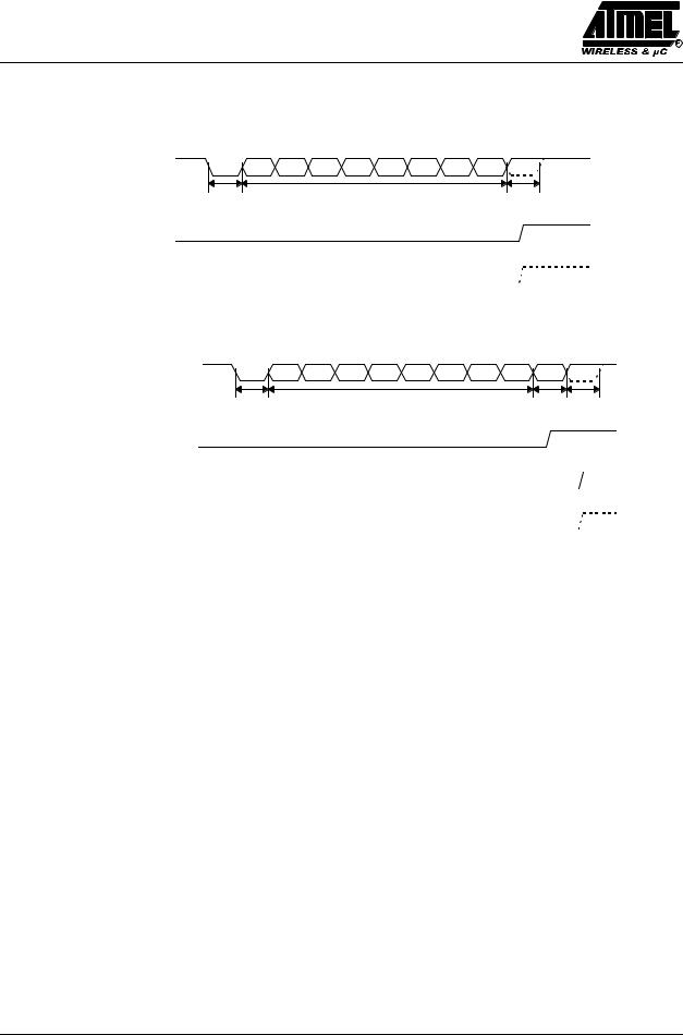
TS80C51U2
TS83C51U2
TS87C51U2
Software may examine FE bit after each reception to check for data errors. Once set, only software or a reset can clear FE bit. Subsequently received frames with valid stop bits cannot clear FE bit. When FE feature is enabled, RI rises on stop bit instead of the last data bit (See Figure 7. and Figure 8.).
RXD |
D0 |
D1 |
D2 |
D3 |
D4 |
D5 |
D6 |
D7 |
|
Start |
Data byte |
Stop |
|
bit |
|
bit |
RI |
|
|
|
SMOD0=X |
|
|
|
FE |
|
|
|
SMOD0=1 |
|
|
|
|
|
|
|
Figure 7. UART Timings in Mode 1
RXD |
D0 |
D1 |
D2 |
D3 |
D4 |
D5 |
D6 |
D7 |
D8 |
|
Start |
Data byte |
Ninth Stop |
||
|
bit |
|
bit bit |
||
RI |
|
|
|
|
|
SMOD0=0 |
|
|
|
|
|
RI |
|
|
|
|
|
|
|
|
|
||
SMOD0=1 |
|
|
|
|
|
|
|
|
|
|
|
FE |
|
|
|
|
|
SMOD0=1 |
|
|
|
|
|
|
|
|
|
|
|
Figure 8. UART Timings in Modes 2 and 3
7.4.2 Automatic Address Recognition
The automatic address recognition feature is enabled for each UART when the multiprocessor communication feature is enabled (SM2 bit in SCON register is set).
Implemented in hardware, automatic address recognition enhances the multiprocessor communication feature by allowing the serial port to examine the address of each incoming command frame. Only when the serial port recognizes its own address, the receiver sets RI bit in SCON register to generate an interrupt. This ensures that the CPU is not interrupted by command frames addressed to other devices.
If desired, you may enable the automatic address recognition feature in mode 1. In this configuration, the stop bit takes the place of the ninth data bit. Bit RI is set only when the received command frame address matches the device’s address and is terminated by a valid stop bit.
To support automatic address recognition, a device is identified by a given address and a broadcast address.
NOTE: The multiprocessor communication and automatic address recognition features cannot be enabled in mode 0 (i.e. setting SM2 bit in SCON register in mode 0 has no effect).
7.4.3 Given Address
Each UART has an individual address that is specified in SADDR_0 or SADDR_1 register; the SADEN_0 or SADEN_1 register is a mask byte that contains don’t-care bits (defined by zeros) to form the device’s given address. The don’t-care bits provide the flexibility to address one or more slaves at a time. The following example
20 |
Rev. D - 15 January, 2001 |
TS80C51U2
TS83C51U2
TS87C51U2
illustrates how a given address is formed.
To address a device by its individual address, the SADEN mask byte must be 1111 1111b. For example:
SADDR |
0101 0110b |
SADEN |
1111 1100b |
Given |
0101 01XXb |
The following is an example of how to use given addresses to address different slaves:
Slave A: |
SADDR |
1111 0001b |
|
SADEN |
1111 1010b |
|
Given |
1111 0X0Xb |
Slave B: |
SADDR |
1111 0011b |
|
SADEN |
1111 1001b |
|
Given |
1111 0XX1b |
Slave C: |
SADDR |
1111 0010b |
|
SADEN |
1111 1101b |
|
Given |
1111 00X1b |
The SADEN byte is selected so that each slave may be addressed separately.
For slave A, bit 0 (the LSB) is a don’t-care bit; for slaves B and C, bit 0 is a 1. To communicate with slave A only, the master must send an address where bit 0 is clear (e.g. 1111 0000b).
For slave A, bit 1 is a 1; for slaves B and C, bit 1 is a don’t care bit. To communicate with slaves B and C, but not slave A, the master must send an address with bits 0 and 1 both set (e.g. 1111 0011b).
To communicate with slaves A, B and C, the master must send an address with bit 0 set, bit 1 clear, and bit 2 clear (e.g. 1111 0001b).
7.4.4 Broadcast Address
A broadcast address is formed from the logical OR of the SADDR and SADEN registers with zeros defined as don’t-care bits, e.g.:
SADDR |
0101 0110b |
SADEN |
1111 1100b |
Broadcast =SADDR OR SADEN |
1111 111Xb |
The use of don’t-care bits provides flexibility in defining the broadcast address, however in most applications, a broadcast address is FFh. The following is an example of using broadcast addresses:
Slave A: |
SADDR |
1111 |
0001b |
|
SADEN |
1111 |
1010b |
|
Broadcast |
1111 |
1X11b, |
Slave B: |
SADDR |
1111 |
0011b |
|
SADEN |
1111 |
1001b |
|
Broadcast |
1111 |
1X11B, |
Slave C: |
SADDR= |
1111 |
0010b |
|
SADEN |
1111 |
1101b |
|
Broadcast |
1111 |
1111b |
For slaves A and B, bit 2 is a don’t care bit; for slave C, bit 2 is set. To communicate with all of the slaves, the master must send an address FFh. To communicate with slaves A and B, but not slave C, the master can send and address FBh.
7.4.5 Reset Addresses
On reset, the SADDR and SADEN registers are initialized to 00h, i.e. the given and broadcast addresses are XXXX XXXXb (all don’t-care bits). This ensures that the serial port will reply to any address, and so, that it is backwards compatible with the 80C51 microcontrollers that do not support automatic address recognition.
Rev. D - 15 January, 2001 |
21 |
Loading...