


 Loading...
Am186ä and Am188ä Family
Instruction Set Manual
February, 1997
© 1997 Advanced Micro Devices, Inc.
Advanced Micro Devices reserves the right to make changes in its products without notice in order to improve design or performance characteristics.
This publication neither states nor implies any warranty of any kind, including but not limited to implied warrants of merchantability or fitness for a particular application. AMD assumes no responsibility for the use of any circuitry other than the circuitry in an AMD product.
The information in this publication is believed to be accurate in all respects at the time of publication, but is subject to change without notice. AMD assumes no responsibility for any errors or omissions, and disclaims responsibility for any consequences resulting from the use of the information included herein. Additionally, AMD assumes no responsibility for the functioning of undescribed features or parameters.
Trademarks
AMD, the AMD logo, and combinations thereof are trademarks of Advanced Micro Devices, Inc.
Am186, Am188, and E86 are trademarks of Advanced Micro Devices, Inc.
FusionE86 is a service mark of Advanced Micro Devices, Inc.
Product names used in this publication are for identification purposes only and may be trademarks of their respective companies.

PREFACE
INTRODUCTION AND OVERVIEW
AMD has a strong history in x86 architecture and its E86™ family meets customer requirements of low system cost, high performance, quality vendor reputation, quick time to market, and an easy upgrade strategy.
The 16-bit Am186™ and Am188™ family of microcontrollers is based on the architecture of the original 8086 and 8088 microcontrollers, and currently includes the 80C186, 80C188, 80L186, 80L188, Am186EM, Am186EMLV, Am186ER, Am186ES, Am186ESLV, Am188EM, Am188EMLV, Am188ER, Am188ES, and Am188ESLV. Throughout this manual, the term Am186 and Am188 microcontrollers refers to any of these microcontrollers as well as future members based on the same core.
The Am186EM/ER/ES and Am188EM/ES/ER microcontrollers build on the 80C186/ 80C188 microcontroller cores and offer 386-class performance while lowering system cost. Designers can reduce the cost, size, and power consumption of embedded systems, while increasing performance and functionality. This is achieved by integrating key system peripherals onto the microcontroller. These low-cost, high-performance microcontrollers for embedded systems provide a natural migration path for 80C186/80C188 designs that need performance and cost enhancements.
PURPOSE OF THIS MANUAL
Each member of the Am186 and Am188 family of microcontrollers shares the standard 186 instruction set. This manual describes that instruction set. Details on technical features of family members can be found in the user’s manual for that specific device. Additional information is available in the form of data sheets, application notes, and other documentation provided with software products and hardware-development tools.
INTENDED AUDIENCE
This manual is intended for computer hardware and software engineers and system architects who are designing or are considering designing systems based on the Am186 and Am188 family of microcontrollers.
MANUAL OVERVIEW
The information in this manual is organized into 4 chapters and 1 appendix.
νChapter 1 provides a programming overview of the Am186 and Am188 microcontrollers, including the register set, instruction set, memory organization and address generation, I/O space, segments, data types, and addressing modes.
νChapter 2 offers an instruction set overview, detailing the format of the instructions.
νChapter 3 contains an instruction set listing, both by functional type and in alphabetical order.
νChapter 4 describes in detail each instruction in the Am186 and Am188 microcontrollers instruction set.
νAppendix A provides an instruction set summary table, as well as a guide to the instruction set by hex and binary opcode.
Introduction and Overview |
iii |

AMD DOCUMENTATION
E86 Family
ORDER NO. |
DOCUMENT TITLE |
19168 |
Am186EM and Am188EM Microcontrollers Data Sheet |
|
Hardware documentation for the Am186EM, Am186EMLV, Am188EM, and |
|
Am188EMLV microcontrollers: pin descriptions, functional descriptions, abso- |
|
lute maximum ratings, operating ranges, switching characteristics and wave- |
|
forms, connection diagrams and pinouts, and package physical dimensions. |
20732 |
Am186ER and Am188ER Microcontrollers Data Sheet |
|
Hardware documentation for the Am186ER and Am188ER microcontrollers: pin |
|
descriptions, functional descriptions, absolute maximum ratings, operating rang- |
|
es, switching characteristics and waveforms, connection diagrams and pinouts, |
|
and package physical dimensions. |
20002 |
Am186ES and Am188ES Microcontrollers Data Sheet |
|
Hardware documentation for the Am186ES, Am186ESLV, Am188ES, and |
|
Am188ESLV microcontrollers:pin descriptions,functionaldescriptions,absolute |
|
maximum ratings, operating ranges, switching characteristics and waveforms, |
|
connection diagrams and pinouts, and package physical dimensions. |
20071 |
E86 Family Support Tools Brief |
|
Lists available E86 family software and hardware development tools, as well as |
|
contact information for suppliers. |
19255 |
FusionE86SM Catalog |
|
Provides information on tools that speed an E86 family embedded product to |
|
market. Includes products from expert suppliers of embedded development so- |
|
lutions. |
21058 |
FusionE86 Development Tools Reference CD |
|
Provides a single-source multimedia tool for customer evaluation of AMD prod- |
|
ucts as well as Fusion partner tools and technologies that support the E86 family |
|
of microcontrollers and microprocessors. Technical documentation for the E86 |
|
family is included on the CD in PDF format. |
To order literature, contact the nearest AMD sales office or call 800-222-9323 (in the U.S. and Canada) or direct dial from any location 512-602-5651. Literature is also available in postscript and PDF formats on the AMD web site. To access the AMD home page, go to http:/ /www.amd.com.
iv |
Introduction and Overview |

TABLE OF CONTENTS
PREFACE |
INTRODUCTION AND OVERVIEW |
III |
|
PURPOSE OF THIS MANUAL . . . . . . . . . . . . . . . . . . . . . . . . . . . . . . . . . . . . . . |
III |
|
INTENDED AUDIENCE . . . . . . . . . . . . . . . . . . . . . . . . . . . . . . . . . . . . . . . . . . . . |
III |
|
MANUAL OVERVIEW . . . . . . . . . . . . . . . . . . . . . . . . . . . . . . . . . . . . . . . . . . . . . |
III |
|
AMD DOCUMENTATIONiv |
|
|
E86 Family . . . . . . . . . . . . . . . . . . . . . . . . . . . . . . . . . . . . . . . . . . . . . . . . . |
iv |
CHAPTER 1 PROGRAMMING
1.1 REGISTER SET . . . . . . . . . . . . . . . . . . . . . . . . . . . . . . . . . . . . . . . . . . . . . 1-1 1.1.1 Processor Status Flags Register . . . . . . . . . . . . . . . . . . . . . . . . . 1-2 1.2 INSTRUCTION SET . . . . . . . . . . . . . . . . . . . . . . . . . . . . . . . . . . . . . . . . . . 1-3
1.3 MEMORY ORGANIZATION AND ADDRESS GENERATION . . . . . . . . . . 1-3 1.4 I/O SPACE . . . . . . . . . . . . . . . . . . . . . . . . . . . . . . . . . . . . . . . . . . . . . . . . . 1-5 1.5 SEGMENTS . . . . . . . . . . . . . . . . . . . . . . . . . . . . . . . . . . . . . . . . . . . . . . . . 1-5 1.6 DATA TYPES . . . . . . . . . . . . . . . . . . . . . . . . . . . . . . . . . . . . . . . . . . . . . . . 1-5 1.7 ADDRESSING MODES . . . . . . . . . . . . . . . . . . . . . . . . . . . . . . . . . . . . . . . 1-7
Register and Immediate Operands . . . . . . . . . . . . . . . . . . . . . . . . . . . . . . . 1-7
Memory Operands . . . . . . . . . . . . . . . . . . . . . . . . . . . . . . . . . . . . . . . . . . . |
1-7 |
CHAPTER 2 INSTRUCTION SET OVERVIEW
2.1 OVERVIEW . . . . . . . . . . . . . . . . . . . . . . . . . . . . . . . . . . . . . . . . . . . . . . . . 2-1 2.2 INSTRUCTION FORMAT. . . . . . . . . . . . . . . . . . . . . . . . . . . . . . . . . . . . . . 2-1 2.2.1 Instruction Prefixes . . . . . . . . . . . . . . . . . . . . . . . . . . . . . . . . . . . . 2-1 2.2.2 Segment Override Prefix . . . . . . . . . . . . . . . . . . . . . . . . . . . . . . . 2-2 2.2.3 Opcode . . . . . . . . . . . . . . . . . . . . . . . . . . . . . . . . . . . . . . . . . . . . . 2-2 2.2.4 Operand Address . . . . . . . . . . . . . . . . . . . . . . . . . . . . . . . . . . . . . 2-2 2.2.5 Displacement . . . . . . . . . . . . . . . . . . . . . . . . . . . . . . . . . . . . . . . . 2-3 2.2.6 Immediate . . . . . . . . . . . . . . . . . . . . . . . . . . . . . . . . . . . . . . . . . . . 2-3 2.3 NOTATION. . . . . . . . . . . . . . . . . . . . . . . . . . . . . . . . . . . . . . . . . . . . . . . . . 2-3
2.4 USING THIS manual . . . . . . . . . . . . . . . . . . . . . . . . . . . . . . . . . . . . . . . . . 2-4 2.4.1 Mnemonics and Names . . . . . . . . . . . . . . . . . . . . . . . . . . . . . . . . 2-4 2.4.2 Forms of the Instruction . . . . . . . . . . . . . . . . . . . . . . . . . . . . . . . . 2-4 2.4.3 What It Does . . . . . . . . . . . . . . . . . . . . . . . . . . . . . . . . . . . . . . . . . 2-6 2.4.4 Syntax . . . . . . . . . . . . . . . . . . . . . . . . . . . . . . . . . . . . . . . . . . . . . . 2-6 2.4.5 Description . . . . . . . . . . . . . . . . . . . . . . . . . . . . . . . . . . . . . . . . . . 2-6 2.4.6 Operation It Performs . . . . . . . . . . . . . . . . . . . . . . . . . . . . . . . . . . 2-7 2.4.7 Flag Settings After Instruction . . . . . . . . . . . . . . . . . . . . . . . . . . . 2-7 2.4.8 Examples . . . . . . . . . . . . . . . . . . . . . . . . . . . . . . . . . . . . . . . . . . . 2-7 2.4.9 Tips . . . . . . . . . . . . . . . . . . . . . . . . . . . . . . . . . . . . . . . . . . . . . . . . 2-8 2.4.10 Related Instructions . . . . . . . . . . . . . . . . . . . . . . . . . . . . . . . . . . . 2-8
CHAPTER 3 INSTRUCTION SET LISTING
3.1 INSTRUCTION SET BY TYPE. . . . . . . . . . . . . . . . . . . . . . . . . . . . . . . . . . 3-1
3.1.1 Address Calculation and Translation . . . . . . . . . . . . . . . . . . . . . . 3-1
3.1.2 Binary Arithmetic . . . . . . . . . . . . . . . . . . . . . . . . . . . . . . . . . . . . . 3-2
Table of Contents |
v |

3.1.4 Comparison . . . . . . . . . . . . . . . . . . . . . . . . . . . . . . . . . . . . . . . . . 3-3 3.1.5 Control Transfer . . . . . . . . . . . . . . . . . . . . . . . . . . . . . . . . . . . . . . 3-3 3.1.6 Data Movement . . . . . . . . . . . . . . . . . . . . . . . . . . . . . . . . . . . . . . 3-5 3.1.7 Decimal Arithmetic . . . . . . . . . . . . . . . . . . . . . . . . . . . . . . . . . . . . 3-6 3.1.8 Flag . . . . . . . . . . . . . . . . . . . . . . . . . . . . . . . . . . . . . . . . . . . . . . . . 3-7 3.1.9 Input/Output . . . . . . . . . . . . . . . . . . . . . . . . . . . . . . . . . . . . . . . . . 3-8 3.1.10 Logical Operation . . . . . . . . . . . . . . . . . . . . . . . . . . . . . . . . . . . . . 3-8 3.1.11 Processor Control . . . . . . . . . . . . . . . . . . . . . . . . . . . . . . . . . . . . . 3-9 3.1.12 String . . . . . . . . . . . . . . . . . . . . . . . . . . . . . . . . . . . . . . . . . . . . . . 3-9
3.2 INSTRUCTION SET in alphabetical order . . . . . . . . . . . . . . . . . . . . . . . . 3-11
CHAPTER 4 INSTRUCTION SET |
|
|
4.1 INSTRUCTIONS . . . . . . . . . . . . . . . . . . . . . . . . . . . . . . . . . . . . . . . . . . . |
. 4-1 |
|
AAA |
ASCII Adjust AL After Addition..................................................... |
4-2 |
AAD |
ASCII Adjust AX Before Division.................................................. |
4-4 |
AAM |
ASCII Adjust AL After Multiplication ............................................. |
4-6 |
AAS |
ASCII Adjust AL After Subtraction................................................ |
4-8 |
ADC |
Add Numbers with Carry ............................................................ |
4-10 |
ADD |
Add Numbers ............................................................................ |
4-14 |
AND |
Logical AND ............................................................................... |
4-17 |
BOUND |
Check Array Index Against Bounds ........................................... |
4-19 |
CALL |
Call Procedure ........................................................................... |
4-21 |
CBW |
Convert Byte Integer to Word..................................................... |
4-24 |
CLC |
Clear Carry Flag......................................................................... |
4-26 |
CLD |
Clear Direction Flag ................................................................... |
4-29 |
CLI |
Clear Interrupt-Enable Flag........................................................ |
4-31 |
CMC |
Complement Carry Flag ............................................................. |
4-33 |
CMP |
Compare Components ............................................................... |
4-34 |
CMPS |
Compare String Components..................................................... |
4-36 |
CWD |
Convert Word Integer to Doubleword......................................... |
4-40 |
DAA |
Decimal Adjust AL After Addition ............................................... |
4-42 |
DAS |
Decimal Adjust AL After Subtraction .......................................... |
4-45 |
DEC |
Decrement Number by One ....................................................... |
4-48 |
DIV |
Divide Unsigned Numbers ......................................................... |
4-50 |
ENTER |
Enter High-Level Procedure....................................................... |
4-53 |
ESC |
Escape ....................................................................................... |
4-56 |
HLT |
Halt............................................................................................. |
4-57 |
IDIV |
Divide Integers ........................................................................... |
4-60 |
IMUL |
Multiply Integers ......................................................................... |
4-63 |
IN |
Input Component from Port........................................................ |
4-67 |
INC |
Increment Number by One......................................................... |
4-69 |
INS |
Input String Component from Port ............................................. |
4-71 |
INT |
Generate Interrupt...................................................................... |
4-73 |
IRET |
Interrupt Return .......................................................................... |
4-76 |
JA |
Jump If Above ............................................................................ |
4-78 |
JAE |
Jump If Above or Equal.............................................................. |
4-80 |
JB |
Jump If Below............................................................................. |
4-82 |
JBE |
Jump If Below or Equal .............................................................. |
4-84 |
JC |
Jump If Carry.............................................................................. |
4-86 |
JCXZ |
Jump If CX Register Is Zero....................................................... |
4-87 |
JE |
Jump If Equal ............................................................................. |
4-89 |
vi |
Table of Contents |

JG |
Jump If Greater .......................................................................... |
4-91 |
JGE |
Jump If Greater or Equal............................................................ |
4-93 |
JL |
Jump If Less............................................................................... |
4-95 |
JLE |
Jump If Less or Equal ................................................................ |
4-97 |
JMP |
Jump Unconditionally ................................................................. |
4-99 |
JNA |
Jump If Not Above.................................................................... |
4-102 |
JNAE |
Jump If Not Above or Equal ..................................................... |
4-103 |
JNB |
Jump If Not Below .................................................................... |
4-104 |
JNBE |
Jump If Not Below or Equal...................................................... |
4-105 |
JNC |
Jump If Not Carry ..................................................................... |
4-106 |
JNE |
Jump If Not Equal..................................................................... |
4-107 |
JNG |
Jump If Not Greater.................................................................. |
4-109 |
JNGE |
Jump If Not Greater or Equal ................................................... |
4-110 |
JNL |
Jump If Not Less ...................................................................... |
4-111 |
JNLE |
Jump If Not Less or Equal........................................................ |
4-112 |
JNO |
Jump If Not Overflow................................................................ |
4-113 |
JNP |
Jump If Not Parity..................................................................... |
4-115 |
JNS |
Jump If Not Sign....................................................................... |
4-116 |
JNZ |
Jump If Not Zero ...................................................................... |
4-118 |
JO |
Jump If Overflow ...................................................................... |
4-119 |
JP |
Jump If Parity ........................................................................... |
4-121 |
JPE |
Jump If Parity Even .................................................................. |
4-122 |
JPO |
Jump If Parity Odd ................................................................... |
4-124 |
JS |
Jump If Sign ............................................................................. |
4-126 |
JZ |
Jump If Zero ............................................................................. |
4-128 |
LAHF |
Load AH with Flags .................................................................. |
4-129 |
LDS |
Load DS with Segment and Register with Offset ..................... |
4-131 |
LEA |
Load Effective Address ........................................................... |
4-133 |
LEAVE |
Leave High-Level Procedure.................................................... |
4-135 |
LES |
Load ES with Segment and Register with Offset .......................... |
4-138 |
LOCK |
Lock the Bus ............................................................................ |
4-140 |
LODS |
Load String Component ........................................................... |
4-141 |
LOOP |
Loop While CX Register Is Not Zero ........................................ |
4-146 |
LOOPE |
Loop If Equal ............................................................................ |
4-148 |
LOOPNE |
Loop If Not Equal ..................................................................... |
4-150 |
LOOPZ |
Loop If Zero.............................................................................. |
4-152 |
MOV |
Move Component..................................................................... |
4-153 |
MOVS |
Move String Component .......................................................... |
4-156 |
MUL |
Multiply Unsigned Numbers ..................................................... |
4-160 |
NEG |
Two’s Complement Negation ................................................... |
4-163 |
NOP |
No Operation............................................................................ |
4-165 |
NOT |
One’s Complement Negation ................................................... |
4-167 |
OR |
Logical Inclusive OR ................................................................ |
4-169 |
OUT |
Output Component to Port ....................................................... |
4-171 |
OUTS |
Output String Component to Port............................................. |
4-173 |
POP |
Pop Component from Stack ..................................................... |
4-175 |
POPA |
Pop All 16-Bit General Registers from Stack................................ |
4-178 |
POPF |
Pop Flags from Stack............................................................... |
4-180 |
PUSH |
Push Component onto Stack ................................................... |
4-181 |
|
|
|
|
Table of Contents |
vii |

PUSHA |
Push All 16-Bit General Registers onto Stack.......................... |
4-184 |
PUSHF |
Push Flags onto Stack ............................................................. |
4-186 |
RCL |
Rotate through Carry Left......................................................... |
4-187 |
RCR |
Rotate through Carry Right ...................................................... |
4-189 |
REP |
Repeat...................................................................................... |
4-191 |
REPE |
Repeat While Equal ................................................................. |
4-193 |
REPNE |
Repeat While Not Equal........................................................... |
4-197 |
REPZ |
Repeat While Zero ................................................................... |
4-201 |
RET |
Return from Procedure............................................................. |
4-202 |
ROL |
Rotate Left................................................................................ |
4-205 |
ROR |
Rotate Right ............................................................................. |
4-207 |
SAHF |
Store AH in Flags ..................................................................... |
4-209 |
SAL |
Shift Arithmetic Left .................................................................. |
4-211 |
SAR |
Shift Arithmetic Right................................................................ |
4-214 |
SBB |
Subtract Numbers with Borrow ................................................ |
4-216 |
SCAS |
Scan String for Component...................................................... |
4-219 |
SHL |
Shift Left ................................................................................... |
4-224 |
SHR |
Shift Right................................................................................. |
4-225 |
STC |
Set Carry Flag .......................................................................... |
4-228 |
STD |
Set Direction Flag..................................................................... |
4-231 |
STI |
Set Interrupt-Enable Flag ......................................................... |
4-235 |
STOS |
Store String Component........................................................... |
4-237 |
SUB |
Subtract Numbers .................................................................... |
4-240 |
TEST |
Logical Compare ...................................................................... |
4-243 |
WAIT |
Wait for Coprocessor ............................................................... |
4-245 |
XCHG |
Exchange Components............................................................ |
4-246 |
XLAT |
Translate Table Index to Component....................................... |
4-248 |
XOR |
Logical Exclusive OR ............................................................... |
4-251 |
APPENDIX A INSTRUCTION SET SUMMARY
INDEX
viii |
Table of Contents |

LIST OF FIGURES
Figure 1-1 |
Register Set . . . . . . . . . . . . . . . . . . . . . . . . . . . . . . . . . . . . . . . . . . . . . . . . . . . . . . . . . . |
1-2 |
Figure 1-2 Processor Status Flags Register (FLAGS) . . . . . . . . . . . . . . . . . . . . . . . . . . . . . . . . . . |
1-2 |
|
Figure 1-3 |
Physical-Address Generation . . . . . . . . . . . . . . . . . . . . . . . . . . . . . . . . . . . . . . . . . . . . . |
1-4 |
Figure 1-4 Memory and i/O Space . . . . . . . . . . . . . . . . . . . . . . . . . . . . . . . . . . . . . . . . . . . . . . . . . |
1-4 |
|
Figure 1-5 Supported Data Types . . . . . . . . . . . . . . . . . . . . . . . . . . . . . . . . . . . . . . . . . . . . . . . . . . |
1-6 |
|
Figure 2-1 |
Instruction Mnemonic and Name Sample . . . . . . . . . . . . . . . . . . . . . . . . . . . . . . . . . . . |
2-4 |
Figure 2-2 |
Instruction Forms Table Sample . . . . . . . . . . . . . . . . . . . . . . . . . . . . . . . . . . . . . . . . . . |
2-4 |
LIST OF TABLES
Table 1-1 Segment Register Selection Rules . . . . . . . . . . . . . . . . . . . . . . . . . . . . . . . . . . . . . . . |
. 1-5 |
|
Table 1-2 Memory Addressing Mode Examples . . . . . . . . . . . . . . . . . . . . . . . . . . . . . . . . . . . . . |
. 1-7 |
|
Table 2-1 |
mod field . . . . . . . . . . . . . . . . . . . . . . . . . . . . . . . . . . . . . . . . . . . . . . . . . . . . . . . . . . . . |
. 2-2 |
Table 2-2 |
aux field . . . . . . . . . . . . . . . . . . . . . . . . . . . . . . . . . . . . . . . . . . . . . . . . . . . . . . . . . . . . |
. 2-3 |
Table 2-3 |
r/m field . . . . . . . . . . . . . . . . . . . . . . . . . . . . . . . . . . . . . . . . . . . . . . . . . . . . . . . . . . . . |
. 2-3 |
Table 3-4 |
Instruction Set . . . . . . . . . . . . . . . . . . . . . . . . . . . . . . . . . . . . . . . . . . . . . . . . . . . . . . . |
3-11 |
Table of Contents |
ix |

x |
Table of Contents |
CHAPTER
1 PROGRAMMING
All members of the Am186 and Am188 family of microcontrollers contain the same basic set of registers, instructions, and addressing modes, and are compatible with the original industry-standard 186/188 parts.
1.1REGISTER SET
The base architecture for Am186 and Am188 microcontrollers has 14 registers (see Figure 1-1), which are controlled by the instructions detailed in this manual. These registers are grouped into the following categories.
νGeneral Registers—Eight 16-bit general purpose registers can be used for arithmetic and logical operands. Four of these (AX, BX, CX, and DX) can be used as 16-bit registers or split into pairs of separate 8-bit registers (AH, AL, BH, BL, CH, CL, DH, and DL). The Destination Index (DI) and Source Index (SI) general-purpose registers are used for data movement and string instructions. The Base Pointer (BP) and Stack Pointer (SP) general-purpose registers are used for the stack segment and point to the bottom and top of the stack, respectively.
–Base and Index Registers—Four of the general-purpose registers (BP, BX, DI, and SI) can also be used to determine offset addresses of operands in memory. These registers can contain base addresses or indexes to particular locations within a segment. The addressing mode selects the specific registers for operand and address calculations.
–Stack Pointer Register—All stack operations (POP, POPA, POPF, PUSH, PUSHA, PUSHF) utilize the stack pointer. The Stack Pointer (SP) register is always offset from the Stack Segment (SS) register, and no segment override is allowed.
νSegment Registers—Four 16-bit special-purpose registers (CS, DS, ES, and SS) select, at any given time, the segments of memory that are immediately addressable for code (CS), data (DS and ES), and stack (SS) memory.
νStatus and Control Registers—Two 16-bit special-purpose registers record or alter certain aspects of the processor state—the Instruction Pointer (IP) register contains the offset address of the next sequential instruction to be executed and the Processor Status Flags (FLAGS) register contains status and control flag bits (see Figure 1-2).
Note that all members of the Am186 and Am188 family of microcontrollers have additional peripheral registers, which are external to the processor. These peripheral registers are not directly accessible by the instruction set. However, because the processor treats these peripheral registers like memory, instructions that have operands that access memory can also access peripheral registers. The above processor registers, as well as the additional peripheral registers, are described in the user’s manual for each specific part.
Programming |
1-1 |

Figure 1-1 |
|
Register Set |
|
|
|
|
|
|
|
||||
16-Bit |
|
|
|
|
|
|
Special |
16-Bit |
|
|
|||
Register |
|
7 |
0 7 |
0 |
|
Register |
Register |
|
|
||||
Name |
|
|
Functions |
Name 15 |
0 |
|
|||||||
Byte |
|
|
AX |
|
AH |
|
AL |
|
Multiply/Divide |
CS |
|
|
Code Segment |
|
|
|
|
|
|
|
|||||||
|
|
|
|
|
|
||||||||
Addressable |
|
DX |
|
DH |
|
DL |
|
I/O Instructions |
DS |
|
|
||
|
|
|
|
|
|
|
|||||||
(8-Bit |
|
|
CX |
|
|
|
|
|
Loop/Shift/Repeat/Count SS |
|
|
Data Segment |
|
Register |
|
|
|
CH |
|
CL |
|
|
|
Stack Segment |
|||
|
|
|
|
||||||||||
Names |
|
|
BX |
|
BH |
|
BL |
|
Base Registers |
ES |
|
|
|
|
|
|
|
|
|
|
|
||||||
Shown) |
|
|
|
|
|
|
Extra Segment |
||||||
BP |
|
base pointer |
|
|
|
|
|||||||
|
|
|
|
|
|||||||||
|
|
|
|
|
|
|
Segment Registers |
||||||
|
|
|
|
|
|
|
|
|
|
|
|||
|
|
|
SI |
|
source index |
|
Index Registers |
||||||
|
|
|
|
|
|||||||||
|
|
|
|
|
|
|
|
|
|||||
|
|
|
DI |
|
destination index |
|
15 |
0 |
|
||||
|
|
|
|
|
|
|
|||||||
|
|
|
SP |
|
|
|
|
|
Stack Pointer |
FLAGS |
|
|
Processor Status Flags |
|
|
|
|
|
|
|
|
||||||
|
|
|
|
15 |
General |
0 |
|
|
IP |
|
|
Instruction Pointer |
|
|
|
|
|
|
|
|
|
|
|
|
|||
|
|
|
|
|
|
|
|
|
|
|
|||
Registers
Status and Control
Registers
1.1.1Processor Status Flags Register
The 16-bit processor status flags register (see Figure 1-2) records specific characteristics of the result of logical and arithmetic instructions (bits 0, 2, 4, 6, 7, and 11) and controls the operation of the microcontroller within a given operating mode (bits 8, 9, and 10).
After an instruction is executed, the value of a flag may be set (to 1), cleared/reset (to 0), unchanged, or undefined. The term undefined means that the flag value prior to the execution of the instruction is not preserved, and the value of the flag after the instruction is executed cannot be predicted. The documentation for each instruction indicates how each flag bit is affected by that instruction.
Figure 1-2 Processor Status Flags Register (FLAGS)
15 |
7 |
0 |
Reserved
OF |
|
|
|
|
|
|
|
|
|
|
|
|
|
|
|
|
|
|
|
AF |
|
PF |
|
CF |
|
|
|
|
|
|
|
|
|
|
|
|
|
|
|
|
|
|
|
|
|||||
|
|
|
|
|
|
|
|
|
|
|
|
|
|
|
|
|
|
|
||||||
|
||||||||||||||||||||||||
DF |
|
|
|
|
|
|
|
|
|
|
|
|
|
|
|
Res Res Res |
||||||||
IF |
|
|
|
|
|
|
|
|
|
|
|
|
|
|
|
|
|
|
|
|
|
|||
TF |
|
|
|
|
|
|
|
|
|
|
|
|
|
|
|
|
|
|
|
|
|
|||
|
|
|
|
|
|
|
|
|
|
|
|
|
|
|
|
|
|
|
|
|
||||
SF |
|
|
|
|
|
|
|
|
|
|
|
|
|
|
|
|
|
|
|
|
|
|
||
|
|
|
|
|
|
|
|
|
|
|
|
|
|
|
|
|
|
|
|
|
|
|||
|
|
|
|
|
|
|
|
|
|
|
|
|
|
|
|
|
|
|
|
|
|
|||
ZF |
|
|
|
|
|
|
|
|
|
|
|
|
|
|
|
|
|
|
|
|
|
|||
|
|
|
|
|
|
|
|
|
|
|
|
|
|
|
|
|
|
|
|
|
||||
Bits 15–12 —Reserved.
Bit 11: Overflow Flag (OF)—Set if the signed result cannot be expressed within the number of bits in the destination operand, cleared otherwise.
1-2 |
Programming |

Bit 10: Direction Flag (DF)—Causes string instructions to auto decrement the appropriate index registers when set. Clearing DF causes auto-increment. See the CLD and STD instructions, respectively, for how to clear and set the Direction Flag.
Bit 9: Interrupt-Enable Flag (IF)—When set, enables maskable interrupts to cause the CPU to transfer control to a location specified by an interrupt vector. See the CLI and STI instructions, respectively, for how to clear and set the Interrupt-Enable Flag.
Bit 8: Trace Flag (TF)—When set, a trace interrupt occurs after instructions execute. TF is cleared by the trace interrupt after the processor status flags are pushed onto the stack. The trace service routine can continue tracing by popping the flags back with an IRET instruction.
Bit 7: Sign Flag (SF)—Set equal to high-order bit of result (set to 0 if 0 or positive, 1 if negative).
Bit 6: Zero Flag (ZF)—Set if result is 0; cleared otherwise.
Bit 5: Reserved
Bit 4: Auxiliary Carry (AF)—Set on carry from or borrow to the low-order 4 bits of the AL general-purpose register; cleared otherwise.
Bit 3: Reserved
Bit 2: Parity Flag (PF)—Set if low-order 8 bits of result contain an even number of 1 bits; cleared otherwise.
Bit 1: Reserved
Bit 0: Carry Flag (CF)—Set on high-order bit carry or borrow; cleared otherwise. See the CLC, CMC, and STC instructions, respectively, for how to clear, toggle, and set the Carry Flag. You can use CF to indicate the outcome of a procedure, such as when searching a string for a character. For instance, if the character is found, you can use STC to set CF to 1; if the character is not found, you can use CLC to clear CF to 0. Then, subsequent instructions that do not affect CF can use its value to determine the appropriate course of action.
1.2INSTRUCTION SET
Each member of the Am186 and Am188 family of microcontrollers shares the standard 186 instruction set. An instruction can reference from zero to several operands. An operand can reside in a register, in the instruction itself, or in memory. Specific operand addressing modes are discussed on page 1-7.
Chapter 2 provides an overview of the instruction set, describing the format of the instructions. Chapter 3 lists all the instructions for the Am186 and Am188 microcontrollers in both functional and alphabetical order. Chapter 4 details each instruction.
1.3MEMORY ORGANIZATION AND ADDRESS GENERATION
The Am186 and Am188 microcontrollers organize memory in sets of segments. Memory
is addressed using a two-component address that consists of a 16-bit segment value and a 16-bit offset. Each segment is a linear contiguous sequence of 64K (216) 8-bit bytes of memory in the processor’s address space. The offset is the number of bytes from the beginning of the segment (the segment address) to the data or instruction which is being accessed.
The processor forms the physical address of the target location by taking the segment address, shifting it to the left 4 bits (multiplying by 16), and adding this to the 16-bit offset.
Programming |
1-3 |
The result is a 20-bit address of the target data or instruction. Thisallowsfora 1-Mbyte physical address size.
For example, if the segment register is loaded with 12A4h and the offset is 0022h, the resultant address is 12A62h (see Figure 1-3). To find the result:
1.The segment register contains 12A4h.
2.The segment register is shifted 4 places and is now 12A40h.
3.The offset is 0022h.
4.The shifted segment address (12A40h) is added to the offset (00022h) to get 12A62h.
5.This address is placed on the address bus pins of the controller.
All instructions that address operands in memory must specify (implicitly or explicitly) a 16bit segment value and a 16-bit offset value. The 16-bit segment values are contained in one of four internal segment registers (CS, DS, ES, and SS). See "Addressing Modes” on page 1-7 for more information on calculating the segment and offset values. See "Segments" on page 1-5 for more information on the CS, DS, ES, and SS registers.
In addition to memory space, all Am186 and Am188 microcontrollers provide 64K of I/O space (see Figure 1-4). The I/O space is described on page 1-5.
Figure 1-3 Physical-Address Generation
Shift Left
4 Bits
|
|
|
|
|
|
|
|
1 |
|
|
2 |
A |
4 |
Segment |
|
|
|
|
|
|
|
|
|
|
|
|
|
|
|
||||||
|
|
|
|
|
|
|
|
|
|
|
|
||||||
|
|
|
|
|
|
|
|
|
|
Base |
|
|
|||||
|
|
|
|
|
|
|
|
|
|
|
|
|
|
|
|
|
|
|
|
|
|
|
|
|
15 |
|
|
|
|
0 |
|
Logical Address |
|||
|
|
|
|
|
|
|
|
|
|
|
|
|
|||||
|
|
|
|
|
|
|
|
|
|
|
|
|
|
|
|
|
|
|
|
|
|
|
|
|
|
|
|
|
|
|
|
|
|
|
|
|
|
|
|
|
|
|
|
0 |
|
|
0 |
2 |
2 |
Offset |
|
|
|
|
|
|
|
|
|
|
|
|
|
|
|
|
|
|
|
|
|
|
|
|
|
|
|
|
|
15 |
|
|
|
|
0 |
|
|
|
|
1 |
|
2 |
A |
4 |
|
|
0 |
|
|
|
|
|
|
|
|
|
|
|
|
|
|
|
|
|
|
||||||||||
|
|
|
|
|
|
|
|
|
|
|
|
|
|
|
|
|
|
19 |
|
|
|
|
0 |
|
|
|
|
|
|
|
|
||||
|
|
|
|
|
|
|
|
|
|
|
|
|
|
|
|
|
|
0 |
|
0 |
0 |
2 |
|
2 |
|
|
|
|
|
|
|
|
|
||
|
|
|
|
|
|
|
|
|
|||||||||
|
|
|
|
|
|
|
|
|
|||||||||
|
|
|
|
|
|
|
|
|
|
|
|
|
|
|
|
|
|
|
|
|
15 |
|
|
0 |
|
|
|
|
|
|
|
|
|
||
|
|
|
|
|
|
|
|
|
|
|
|
|
|
|
|
|
|
1 |
|
2 |
A |
6 |
|
2 |
|
|
|
Physical Address |
|
|
|||||
19 |
|
|
|
|
0 |
|
|
|
|
|
|
|
|
|
|||
|
|
|
|
|
|
|
|
|
|
|
|
|
|||||
|
|
|
|
|
|
|
|
|
|
|
|
|
|
|
|
|
|
|
|
|
|
To Memory |
|
|
|
|
|
|
|
|
|
|
|
||
Figure 1-4 Memory and i/O Space
Memory
Space 1M
I/O
Space 64K
1-4 |
Programming |

1.4I/O SPACE
The I/O space consists of 64K 8-bit or 32K 16-bit ports. The IN and OUT instructions address the I/O space with either an 8-bit port address specified in the instruction, or a 16-bit port address in the DX register. 8-bit port addresses are zero-extended so that A15–A8 are Low. I/O port addresses 00F8h through 00FFh are reserved. The Am186 and Am188 microcontrollers provide specific instructions for addressing I/O space.
1.5SEGMENTS
The Am186 and Am188 microcontrollers use four segment registers:
1.Data Segment (DS): The processor assumes that all accesses to the program’s variables are from the 64K space pointed to by the DS register. The data segment holds data, operands, etc.
2.Code Segment (CS): This 64K space is the default location for all instructions. All code must be executed from the code segment.
3.Stack Segment (SS): The processor uses the SS register to perform operations that involve the stack, such as pushes and pops. The stack segment is used for temporary space.
4.Extra Segment (ES): Usually this segment is used for large string operations and for large data structures. Certain string instructions assume the extra segment as the segment portion of the address. The extra segment is also used (by using segment override) as a spare data segment.
When a segment register is not specified for a data movement instruction, it’s assumed to be a data segment. An instruction prefix can be used to override the segment register (see "Segment Override Prefix" on page 2-2).For speed and compact instruction encoding, the segment register used for physical-address generation is implied by the addressing mode used (see Table 1-1).
Table 1-1 |
Segment Register Selection Rules |
||
Memory Reference Needed |
Segment Register Used |
Implicit Segment Selection Rule |
|
|
|
|
|
Local Data |
|
Data (DS) |
All data references |
|
|
|
|
Instructions |
|
Code (CS) |
Instructions (including immediate data) |
|
|
|
|
Stack |
|
Stack (SS) |
All stack pushes and pops |
|
|
|
Any memory references that use the BP register |
|
|
|
|
External Data (Global) |
Extra (ES) |
All string instruction references that use the DI register as an index |
|
|
|
|
|
1.6DATA TYPES
The Am186 and Am188 microcontrollers directly support the following data types:
νInteger—A signed binary numeric value contained in an 8-bit byte or a 16-bit word. All operations assume a two’s complement representation.
νOrdinal—An unsigned binary numeric value contained in an 8-bit byte or a 16-bit word.
νDouble Word—A signed binary numeric value contained in two sequential 16-bit addresses, or in a DX::AX register pair.
νQuad Word—A signed binary numeric value contained in four sequential 16-bit addresses.
νBCD—An unpacked byte representation of the decimal digits 0–9.
Programming |
1-5 |

νASCII—A byte representation of alphanumeric and control characters using the ASCII standard of character representation.
νPacked BCD—A packed byte representation of two decimal digits (0–9). One digit is stored in each nibble (4 bits) of the byte.
νString—A contiguous sequence of bytes or words. A string can contain from 1 byte up to 64 Kbyte.
νPointer—A 16-bit or 32-bit quantity, composed of a 16-bit offset component or a 16-bit segment base component plus a 16-bit offset component.
In general, individual data elements must fit within defined segment limits. Figure 1-5 graphically represents the data types supported by the Am186 and Am188 microcontrollers.
Figure 1-5 Supported Data Types
Signed |
7 |
|
|
|
|
|
|
|
|
0 |
|
|
|
|
|
|
|
|
|
|
|
|
|
|
|
|
|
|
|
|
|
|
|
|
|
|
|||||
Byte |
|
|
|
|
|
|
|
|
|
|
|
|
|
|
|
|
|
|
|
|
|
|
|
|
|
|
|
|
|
|
|
|
|
|
|
|
|
|
|
||
|
|
|
|
|
|
|
|
|
|
|
|
|
|
|
|
|
|
|
|
|
|
|
|
|
|
|
|
|
|
|
|
|
|
|
|
|
|
|
|||
Sign Bit |
|
|
|
|
|
|
|
|
|
|
|
|
|
|
|
|
|
|
|
|
|
|
|
|
|
|
|
|
|
|
|
|
|
|
|
|
|
|
|
|
|
|
|
|
|
|
|
|
|
|
|
|
|
|
|
|
|
|
|
|
|
|
|
|
|
|
|
|
|
|
|
|
|
|
|
|
|
|
|
|
|
||
|
|
|
|
|
|
|
|
|
|
|
|
|
|
|
|
|
|
|
|
|
|
|
|
|
|
|
|
|
|
|
|
|
|
|
|
|
|
|
|||
|
|
|
|
|
|
|
|
|
|
|
|
|
|
|
|
|
|
|
|
|
|
|
|
|
|
|
|
|
|
|
|
|
|
|
|
|
|
|
|
||
|
|
|
Magnitude |
|
|
|
|
|
|
|
|
|
|
|
|
|
|
|
|
|
|
|
|
|
|
|
|
||||||||||||||
Unsigned |
7 |
|
|
|
|
|
|
|
0 |
|
|
|
|
|
|
|
|
|
|
|
|
|
|
|
|
|
|
|
|
|
|
|
|
|
|
||||||
Byte |
|
|
|
|
|
|
|
|
|
|
|
|
|
|
|
|
|
|
|
|
|
|
|
|
|
|
|
|
|
|
|
|
|
|
|
|
|
|
|
||
|
|
|
|
|
|
|
|
|
|
|
|
|
|
|
|
|
|
|
|
|
|
|
|
|
|
|
|
|
|
|
|
|
|
|
|
|
|
|
|||
|
|
|
|
|
|
|
|
|
|
|
|
|
|
|
|
|
|
|
|
|
|
|
|
|
|
|
|
|
|
|
|
|
|
|
|
|
|
|
|||
|
|
|
|
|
|
|
|
|
|
MSB |
|
|
|
|
|
|
|
|
|
|
|
|
|
|
|
|
|
|
|
|
|
|
|
|
|
|
|||||
|
|
|
|
|
|
|
|
|
|
|
|
|
|
|
|
|
|
|
|
|
|
|
|
|
|
|
|
|
|
|
|
|
|
|
|
||||||
|
|
|
|
|
|
|
|
|
|
|
|
|
|
|
|
|
|
|
|
|
|
|
|
|
|
|
|
|
|
|
|
|
|
|
|||||||
|
|
|
Magnitude |
|
|
|
|
|
|
|
|
|
|
|
|
|
|
|
|
|
|
|
|
|
|
|
|
||||||||||||||
Signed |
1514 |
+1 |
8 7 |
0 |
|
0 |
|
|
|
|
|
|
|
|
|
|
|
|
|
|
|
|
|
||||||||||||||||||
Word |
|
|
|
|
|
|
|
|
|
|
|
|
|
|
|
|
|
|
|
|
|
|
|
|
|
||||||||||||||||
|
|
|
|
|
|
|
|
|
|
|
|
|
|
|
|
|
|
|
|
|
|
|
|
|
|
|
|
|
|
|
|
|
|
|
|
|
|
|
|||
|
|
|
|
|
|
|
|
|
|
|
|
|
|
|
|
|
|
|
|
|
|
|
|
|
|
|
|
|
|
|
|
|
|
|
|
|
|
|
|||
Sign Bit |
|
|
|
|
|
|
|
|
|
|
|
|
|
|
|
|
|
|
|
|
|
|
|
|
|
|
|
|
|
|
|
|
|
|
|
|
|
|
|
||
|
|
|
|
|
|
|
|
|
MSB |
|
|
|
|
|
|
|
|
|
|
|
|
|
|
|
|
|
|
|
|
|
|
|
|
||||||||
|
|
|
|
|
|
|
|
|
|
|
|
|
|
|
|
|
|
|
|
|
|
|
|
|
|
|
|
|
|
|
|
|
|||||||||
|
|
|
|
|
|
|
|
|
|
|
|
|
|
|
|
|
|
|
|
|
|
|
|
|
|
|
|
|
|
|
|
|
|||||||||
|
|
|
|
|
|
|
|
|
|
|
|
|
|
|
|
|
|
|
|
|
|
|
|
|
|
|
|
|
|
|
|
|
|||||||||
|
|
|
|
|
|
|
|
|
|
|
|
Magnitude |
|
|
|
|
|
|
|
|
|
|
|
|
|
|
|
|
|
|
|
||||||||||
Signed |
|
|
|
|
|
|
|
|
+3 |
|
|
|
|
|
+2 |
|
|
|
|
|
+1 |
|
|
|
|
0 |
|
|
|
|
|||||||||||
Double |
31 |
|
|
|
|
|
|
|
|
|
1615 |
|
|
|
|
0 |
|||||||||||||||||||||||||
|
|
|
|
|
|
|
|
|
|
|
|
|
|
|
|
|
|
|
|
|
|
|
|
|
|
||||||||||||||||
Word |
|
|
|
|
|
|
|
|
|
|
|
|
|
|
|
|
|
|
|
|
|
|
|
|
|
|
|
|
|
|
|
|
|
|
|
|
|
|
|
||
|
|
|
|
|
|
|
|
|
|
|
|
|
|
|
|
|
|
|
|
|
|
|
|
|
|
|
|
|
|
|
|
|
|
|
|
|
|
|
|||
|
|
|
|
|
|
|
|
|
|
|
|
|
|
|
|
|
|
|
|
|
|
|
|
|
|
|
|
|
|
|
|
|
|
|
|
|
|
|
|||
Sign Bit |
|
|
|
|
|
|
|
|
MSB |
|
|
|
|
|
|
|
|
|
|
|
|
|
|
|
|
|
|
|
|
|
|
|
|
||||||||
|
|
|
|
|
|
|
|
|
|
|
|
|
|
|
|
|
|
|
|
|
|
|
|
|
|
|
|
|
|
|
|
||||||||||
|
|
|
|
|
|
|
|
|
|
|
|
|
|
|
|
|
|
|
|
|
|
|
|
|
|
|
|
|
|
|
|
||||||||||
|
|
|
|
|
|
|
|
|
|
|
|
|
|
|
|
|
|
|
Magnitude |
|
|
|
|
|
|
|
|
|
|
|
|||||||||||
Signed |
+7 |
|
|
+6 |
|
+5 |
|
|
+4 |
|
|
+3 |
|
+2 |
+1 |
+0 |
|
||||||||||||||||||||||||
Quad |
|
|
|
|
|
|
|
|
|
||||||||||||||||||||||||||||||||
63 |
|
|
|
|
|
|
48 47 |
|
|
|
32 31 |
|
|
|
16 15 |
|
|
0 |
|||||||||||||||||||||||
Word |
|
|
|
|
|
|
|
|
|
|
|
|
|
|
|
|
|
|
|
|
|
|
|
|
|
|
|
|
|
|
|
|
|
|
|
|
|
|
|
||
Sign Bit |
|
|
|
|
|
|
|
|
|
MSB |
|
|
|
|
|
|
|
|
|
|
|
|
|
|
|
|
|
|
|
|
|
|
|
|
|||||||
|
|
|
|
|
|
|
|
|
|
|
|
|
|
|
|
|
|
|
|
|
|
|
|
|
|
|
|
|
|
|
|
||||||||||
|
|
|
|
|
|
|
|
|
|
|
|
|
|
|
|
|
|
|
|
|
|
|
|
|
|
|
|
|
|
|
|
|
|||||||||
|
|
|
|
|
|
|
|
|
|
|
|
|
|
|
|
|
|
|
|
|
|
|
|
|
|
|
|
|
|
|
|
||||||||||
|
|
|
|
|
|
|
|
|
|
|
|
|
|
|
|
|
|
Magnitude |
|
|
|
|
|
|
|
|
|
|
|
||||||||||||
Unsigned |
15 |
|
|
|
+1 |
|
|
|
|
|
0 |
|
0 |
|
|
|
|
|
|
|
|
|
|
|
|
|
|
|
|
||||||||||||
|
|
|
|
|
|
|
|
|
|
|
|
|
|
|
|
|
|
|
|
|
|
|
|
|
|
|
|
|
|
|
|||||||||||
|
|
|
|
|
|
|
|
|
|
|
|
|
|
|
|
|
|
|
|
|
|
|
|
|
|
|
|
|
|
|
|
|
|
|
|
|
|
|
|||
Word |
|
|
|
|
|
|
|
|
|
|
|
|
|
|
|
|
|
|
|
|
|
|
|
|
|
|
|
|
|
|
|
|
|
|
|
|
|
|
|
||
|
|
|
|
|
|
|
|
|
|
|
|
|
|
|
|
|
|
|
|
|
|
|
|
|
|
|
|
|
|
|
|
|
|
|
|
|
|
|
|||
|
|
|
|
|
|
|
MSB |
|
|
|
|
|
|
|
|
|
|
|
|
|
|
|
|
|
|
|
|
|
|
|
|
||||||||||
|
|
|
|
|
|
|
|
|
|
|
|
|
|
|
|
|
|
|
|
|
|
|
|
|
|
|
|
|
|
|
|||||||||||
|
|
|
|
|
|
|
|
|
|
|
|
|
|
|
|
|
|
|
|
|
|
|
|
|
|
|
|
|
|
|
|
|
|
||||||||
|
|
|
|
|
|
|
|
|
|
|
|
|
|
|
|
|
|
|
|
|
|
|
|
|
|
|
|
|
|
|
|
|
|
||||||||
|
|
|
|
|
|
|
|
|
|
|
Magnitude |
|
|
|
|
|
|
|
|
|
|
|
|
|
|
|
|
|
|
|
|||||||||||
Binary 7 |
|
|
+N |
0 |
|
|
7 |
+1 |
|
|
0 7 |
|
0 |
|
|
0 |
|
|
||||||||||||||||||
Coded |
|
|
|
|
|
|
|
|
|
|
|
|
. . . |
|
|
|
|
|
|
|
|
|
|
|
|
|
|
|
|
|
|
|
|
|
||
|
|
|
|
|
|
|
|
|
|
|
|
|
|
|
|
|
|
|
|
|
|
|
|
|
|
|
|
|
|
|
|
|
||||
Decimal |
|
|
|
|
|
|
|
|
|
|
|
|
|
|
|
|
|
|
|
|
|
|
|
|
|
|
|
|
|
|
|
|
|
|||
|
|
|
|
BCD |
|
|
|
|
|
|
|
|
|
|
BCD |
|
|
|
|
BCD |
|
|
|
|||||||||||||
(BCD) |
Digit N |
|
|
|
|
|
|
Digit 1 Digit 0 |
|
|
|
|||||||||||||||||||||||||
7 |
|
|
+N |
0 |
|
|
7 |
+1 |
|
|
0 7 |
|
0 |
|
|
0 |
|
|
||||||||||||||||||
|
|
|
|
|
|
|
|
|
|
|
|
|
|
|
|
|
|
|
|
|
|
|||||||||||||||
ASCII |
|
|
|
|
|
|
|
|
|
|
. . . |
|
|
|
|
|
|
|
|
|
|
|
|
|
|
|
|
|
|
|
|
|||||
|
|
|
|
|
|
|
|
|
|
|
|
|
|
|
|
|
|
|
|
|
|
|
|
|
|
|
|
|
||||||||
|
|
|
|
|
|
|
|
|
|
|
|
|
|
|
|
|
|
|
|
|
|
|
|
|
|
|
|
|
||||||||
|
|
|
|
|
ASCII |
|
|
|
|
|
|
|
ASCII |
|
|
|
|
|
ASCII |
|||||||||||||||||
CharacterN |
|
|
|
Character1 Character0 |
||||||||||||||||||||||||||||||||
7 |
|
|
+N |
0 |
|
|
7 |
+1 |
|
|
0 7 |
|
0 |
|
|
0 |
|
|||||||||||||||||||
|
|
|
|
|
|
|
|
|
|
|
|
|
|
|
|
|
|
|
|
|
||||||||||||||||
Packed |
|
|
|
|
|
|
|
|
|
|
. . . |
|
|
|
|
|
|
|
|
|
|
|
|
|
|
|
|
|
|
|
|
|
||||
|
|
|
|
|
|
|
|
|
|
|
|
|
|
|
|
|
|
|
|
|
|
|
|
|
|
|
|
|
|
|
||||||
BCD |
|
|
|
|
|
|
|
|
|
|
|
|
|
|
|
|
|
|
|
|
|
|
|
|
|
|
|
|
|
|
|
|||||
|
|
|
|
|
|
|
|
|
|
|
|
|
|
|
|
|
|
|
|
|
|
|
|
|
|
|
|
|
|
|
|
|
|
|||
|
|
|
|
|
|
|
|
|
|
|
|
|
|
|
|
|
|
|
|
|
|
|
|
|
|
|
|
|
|
|
|
|
|
|||
Most |
|
|
|
|
|
|
|
|
|
|
|
|
|
|
|
|
|
|
|
|
|
Least |
||||||||||||||
Significant Digit |
|
|
Significant Digit |
|||||||||||||||||||||||||||||||||
7 |
|
|
+N |
0 |
|
|
7 |
+1 |
|
0 7 |
|
0 |
|
|
0 |
|
|
|||||||||||||||||||
String |
|
|
|
|
|
|
|
|
|
|
. . . |
|
|
|
|
|
|
|
|
|
|
|
|
|
|
|
|
|
|
|
|
|
||||
|
|
|
|
|
|
|
|
|
|
|
|
|
|
|
|
|
|
|
|
|
|
|
|
|
|
|
|
|
||||||||
|
|
|
|
|
|
|
|
|
|
|
|
|
|
|
|
|
|
|
|
|
|
|
|
|
|
|
|
|
||||||||
Byte/WordN |
|
|
Byte/Word1 Byte/Word0 |
|||||||||||||||||||||||||||||||||
|
|
|
|
+3 |
|
|
|
|
|
+2 |
|
|
|
+1 |
|
|
|
|
|
0 |
|
|
|
|
|
|||||||||||
Pointer |
|
|
|
|
|
|
|
|
|
|
|
|
|
|
|
|
|
|
|
|
|
|
|
|
|
|
|
|
|
|
|
|
|
|
|
|
|
|
|
|
|
|
|
|
|
|
|
|
|
|
|
|
|
|
|
|
|
|
|
|
|
|
|
|
|
|
|
|
|
|
|
||
|
|
|
|
|
|
|
|
|
|
|
|
|
|
|
|
|
|
|
|
|
|
|
|
|
|
|
|
|
|
|
|
|
|
|
||
|
|
|
|
|
|
|
|
|
|
|
|
|
|
|
|
|
|
|
|
|
|
|
|
|
|
|
|
|
|
|
|
|
|
|
||
|
|
|
|
|
|
|
|
|
|
|
|
|
|
|
|
|
|
|
|
|
|
|
|
|
|
|
|
|
|
|
||||||
|
|
|
|
Segment Base |
|
|
|
|
|
|
Offset |
|
|
|
||||||||||||||||||||||
1-6 |
Programming |

1.7ADDRESSING MODES
The Am186 and Am188 microcontrollers use eight categories of addressing modes to specify operands. Two addressing modes are provided for instructions that operate on register or immediate operands; six modes are provided to specify the location of an operand in a memory segment.
Register and Immediate Operands
1.Register Operand Mode—The operand is located in one of the 8- or 16-bit registers.
2.Immediate Operand Mode—The operand is included in the instruction.
Memory Operands
A memory-operand address consists of two 16-bit components: a segment value and an offset. The segment value is supplied by a 16-bit segment register either implicitly chosen by the addressing mode (described below) or explicitly chosen by a segment override prefix (see "Segment Override Prefix" on page 2-2). The offset, also called the effective address, is calculated by summing any combination of the following three address elements:
νDisplacement—an 8-bit or 16-bit immediate value contained in the instruction
νBase—contents of either the BX or BP base registers
νIndex—contents of either the SI or DI index registers
Any carry from the 16-bit addition is ignored. Eight-bit displacements are sign-extended to 16-bit values.
Combinations of the above three address elements define the following six memory addressing modes (see Table 1-2 for examples).
1.Direct Mode—The operand offset is contained in the instruction as an 8- or 16-bit displacement element.
2.Register Indirect Mode—The operand offset is in one of the BP, BX, DI, or SI registers.
3.Based Mode—The operand offset is the sum of an 8- or 16-bit displacement and the contents of a base register (BP or BX).
4.Indexed Mode—The operand offset is the sum of an 8- or 16-bit displacement and the contents of an index register (DI or SI).
5.Based Indexed Mode—The operand offset is the sum of the contents of a base register (BP or BX) and an index register (DI or SI).
6.Based Indexed Mode with Displacement—The operand offset is the sum of a base register’s contents, an index register’s contents, and an 8-bit or 16-bit displacement.
Table 1-2 |
Memory Addressing Mode Examples |
|
|
|
|
|
Addressing Mode |
Example |
|
|
|
|
Direct |
mov ax, ds:4 |
|
|
|
|
Register Indirect |
mov ax, [si] |
|
|
|
|
Based |
mov ax, [bx]4 |
|
|
|
|
Indexed |
mov ax, [si]4 |
|
|
|
|
Based Indexed |
mov ax, [si][bx] |
|
|
|
|
Based Indexed with Displacement |
mov ax, [si][bx]4 |
|
|
|
Programming |
1-7 |

1-8 |
Programming |

CHAPTER
2 INSTRUCTION SET OVERVIEW
2.1OVERVIEW
The instruction set used by the Am186 and Am188 family of microcontrollers is identical to the original 8086 and 8088 instruction set, with the addition of seven instructions (BOUND, ENTER, INS, LEAVE, OUTS, POPA, and PUSHA), and the enhancement of nine instructions (immediate operands were added to IMUL, PUSH, RCL, RCR, ROL, ROR, SAL/SHL, SAR, and SHR). In addition, three valid instructions are not supported with the necessary processor pinout (ESC, LOCK and WAIT). All of these instructions are marked as such in their description.
2.2INSTRUCTION FORMAT
When assembling code, an assembler replaces each instruction statement with its machine-language equivalent. In machine language, all instructions conform to one basic format. However, the length of an instruction in machine language varies depending on the operands used in the instruction and the operation that the instruction performs.
An instruction can reference from zero to several operands. An operand can reside in a register, in the instruction itself, or in memory.
The Am186 and Am188 microcontrollers use the following instruction format. The shortest instructions consist of only a single opcode byte.
Instruction Prefixes
Segment Override Prefix
Opcode
Operand Address
Displacement
Immediate
2.2.1Instruction Prefixes
The REP, REPE, REPZ, REPNE and REPNZ prefixes can be used to repeatedly execute a single string instruction.
The LOCK prefix may be combined with the instruction and segment override prefixes, and causes the processor to assert its bus LOCK signal while the instruction that follows executes.
Instruction Set Overview |
2-1 |
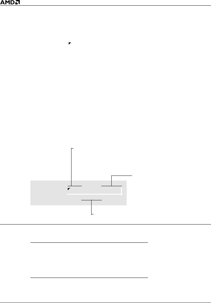
2.2.2Segment Override Prefix
To override the default segment register, place the following byte in front of the instruction, where RR determines which register is used. Only one segment override prefix can be used per instruction.
|
|
|
|
|
|
|
|
|
|
|
|
Segment Override |
0 |
0 |
1 |
|
R |
R |
|
1 |
1 |
0 |
|
Prefix |
7 |
6 |
5 |
|
4 |
3 |
2 |
1 |
0 |
|
|
|
|
|
|||||||||
|
|
|
|
|
|
|
|
|
|
|
|
|
|
|
|
|
|
|
|
|
|
|
|
00 = ES Register
01 = CS Register
10 = SS Register
11 = DS Register
2.2.3Opcode
This specifies the machine-language opcode for an instruction. The format for the opcodes is described on page 2-5. Although most instructions use only one opcode byte, the AAD (D5 0A hex) and AAM (D4 0A hex) instructions use two opcodes.
2.2.4Operand Address
The following illustration shows the structure of the operand address byte. The operand address byte controls the addressing for an instruction.
Along with r/m, the Modifier field determines whether the Register/Memory field is interpreted as a register or the address of a memory operand. For a memory operand, the Modifier field also indicates whether the operand is addressed directly or indirectly. For indirectly addressed memory operands, the Modifier field specifies the number of bytes of displacement that appear in the instruction. See Table 2-1 for mod values.
Along with mod, the Register/Memory field specifies a general register or the address of a memory operand. See Table 2-3 for r/m values.
Operand Address |
mod |
|
aux |
|
|
r/m |
|
|
|
7 |
6 |
5 |
4 |
3 |
2 |
1 |
0 |
The Auxiliary field specifies an opcode extension or a register that is used as a second operand. See Table 2-2 for aux values
Table 2-1 mod field
mod Description
11 r/m is treated as a reg field
00 DISP = 0, disp-low and disp-high are absent
01DISP = disp-low sign-extended to 16-bits, disp-high is absent
10 DISP = disp-high: disp-low
2-2 |
Instruction Set Overview |
Table 2-2 |
aux field |
|
|
|
aux |
If mod=11 and w=0 |
If mod=11 and w=1 |
|
|
|
|
|
000 |
AL |
AX |
|
001 |
CL |
CX |
|
010 |
DL |
DX |
|
011 |
BL |
BX |
|
100 |
AH |
SP |
|
101 |
CH |
BP |
|
110 |
DH |
SI |
|
111 |
BH |
DI |
|
|
|
|
|
* – When mod¹11, depends on instruction |
|
|
Table 2-3 |
r/m field |
|
|
|
|
r/m |
Description |
|
|
|
|
|
000 |
EA* = (BX)+(SI)+DISP |
|
|
001 |
EA = (BX)+(DI)+DISP |
|
|
010 |
EA = (BP)+(SI)+DISP |
|
|
011 |
EA = (BP)+(DI)+DISP |
|
|
100 |
EA = (SI)+DISP |
|
|
101 |
EA = (DI)+DISP |
|
110EA = (BP)+DISP (except if mod=00, then EA = disp-high:disp:low)
111EA = (BX)+DISP
*– EA is the Effective Address
2.2.5Displacement
The displacement is an 8- or 16-bit immediate value to be added to the offset portion of the address.
2.2.6Immediate
The immediate bytes contain up to 16 bits of immediate data.
2.3 |
NOTATION |
|
|
This parameter |
Indicates that |
|
|
|
|
: |
The component on the left is the segment for a component located in |
|
|
memory. The component on the right is the offset. |
|
:: |
The component on the left is concatenated with the component on the right. |
|
|
|
Instruction Set Overview |
2-3 |

2.4USING THIS MANUAL
Each instruction is detailed in Chapter 4. The following sections explain the format used when describing each instruction.
2.4.1Mnemonics and Names
The primary assembly-language mnemonic and its name appear at the top of the first page for an instruction (see Figure 2-1). Some instructions have additional mnemonics that perform the same operation. These synonyms are listed below the primary mnemonic.
Figure 2-1 Instruction Mnemonic and Name Sample
MUL |
Multiply Unsigned Numbers |
2.4.2Forms of the Instruction
Many instructions have more than one form. The forms for each instruction are listed in a table just below the mnemonics (see Figure 2-2).
Figure 2-2 Instruction Forms Table Sample
Form |
Opcode |
Description |
Clocks |
||
Am186 |
Am188 |
||||
|
|
|
|||
|
|
|
|
|
|
MUL r/m8 |
F6 /4 |
AX=(r/m byte)•AL |
26–28/32–34 |
26–28/32–34 |
|
MUL r/m16 |
F7 /4 |
DX::AX=(r/m word)•AX |
35–37/41–43 |
35–37/45–47 |
|
|
|
|
|
|
|
Form
The Form column specifies the syntax for the different forms of an instruction. Each form includes an instruction mnemonic and zero or more operands. Items in italics are placeholders for operands that must be provided. A placeholder indicates the size and type of operand that is allowed.
|
This operand |
Is a placeholder for |
|
|
|
|
|
|
imm8 |
An immediate byte: a signed number between –128 and 127 |
|
|
imm16 |
An immediate word: a signed number between –32768 and 32767 |
|
|
m |
An operand in memory |
|
|
m8 |
A byte string in memory pointed to by DS:SI or ES:DI |
|
|
m16 |
A word string in memory pointed to by DS:SI or ES:DI |
|
|
m16&16 |
A pair of words in memory |
|
|
m16:16 |
A doubleword in memory that contains a full address (segment:offset) |
|
|
moffs8 |
A byte in memory that contains a signed, relative offset displacement |
|
|
moffs16 |
A word in memory that contains a signed, relative offset displacement |
|
|
ptr16:16 |
A full address (segment:offset) |
|
|
r8 |
A general byte register: AL, BL, CL, DL, AH, BH, CH, or DH |
|
|
r16 |
A general word register: AX, BX, CX, DX, BP, SP, DI, or SI |
|
|
r/m8 |
A general byte register or a byte in memory |
|
|
r/m16 |
A general word register or a word in memory |
|
|
rel8 |
A signed, relative offset displacement between –128 and 127 |
|
|
rel16 |
A signed, relative offset displacement between –32768 and 32767 |
|
|
sreg |
A segment register |
|
|
|
|
|
|
|
|
|
2-4 |
Instruction Set Overview |

Opcode
The Opcode column specifies the machine-language opcodes for the different forms of an instruction. (For instruction prefixes, this column also includes the prefix.) Each opcode includes one or more numbers in hexadecimal format, and zero or more parameters, which are shown in italics. A parameter provides information about the contents of the Operand Address byte for that particular form of the instruction.
This parameter |
Indicates that |
|
|
/0–/7 |
The Auxiliary (aux) Field in the Operand Address byte specifies an |
|
extension (from 0 to 7) to the opcode instead of a register. So for example, |
|
the opcode for adding (ADD) an immediate byte to a general byte register |
|
or a byte in memory is "80 /0 ib". So the second byte of the opcode is |
|
"mod 000 r/m", where mod and r/m are as defined in "Operand Address" |
|
on page 2-2. |
/0 |
The aux field is 0. |
/1 |
The aux field is 1. |
/2 |
The aux field is 2. |
/3 |
The aux field is 3. |
/4 |
The aux field is 4. |
/5 |
The aux field is 5. |
/6 |
The aux field is 6. |
/7 |
The aux field is 7. |
/r |
The Auxiliary (aux) field in the Operand Address byte specifies a register |
|
instead of an opcode extension. If the Opcode byte specifies a byte register, |
|
the registers are assigned as follows: AL=0, CL=1, DL=2, BL=3, AH=4, |
|
CH=5, DH=6, and BH=7. If the Opcode byte specifies a word register, the |
|
registers are assigned as follows: AX=0, CX=1, DX=2, BX=3, SP=4, BP=5, |
|
SI=6, and DI=7. |
/sr |
The Auxiliary (aux) field in the Operand Address byte specifies a segment |
|
register as follows: ES=0, CS=1, SS=2, and DS=3. |
cb |
The byte following the Opcode byte specifies an offset. |
cd |
The doubleword following the Opcode byte specifies an offset and, in some |
|
cases, a segment. |
cw |
The word following the Opcode byte specifies an offset and, in some cases, |
|
a segment. |
ib |
The parameter is an immediate byte. The Opcode byte determines whether |
|
it is interpreted as a signed or unsigned number. |
iw |
The parameter is an immediate word. The Opcode byte determines whether |
|
it is interpreted as a signed or unsigned number. |
rb |
The byte register operand is specified in the Opcode byte. To determine |
|
the Opcode byte for a particular register, add the hexadecimal value on the |
|
left of the plus sign to the value of rb for that register, as follows: |
|
AL=0, CL=1, DL=2, BL= 3, AH=4, CH=5, DH=6, and BH=7. So for example, |
|
the opcode for moving an immediate byte to a register (MOV) is "B0+rb". |
|
So B0–B7 are valid opcodes, and B0 is "MOV AL,imm8". |
rw |
The word register operand is specified in the Opcode byte. To determine |
|
the Opcode byte for a particular register, add the hexadecimal value on the |
|
left of the plus sign to the value of rw for that register, as follows: |
|
AX=0, CX=1, DX=2, BX=3, SP=4, BP=5, SI=6, DI=7. |
|
|
Instruction Set Overview |
2-5 |

Description
The Description column contains a brief synopsis of each form of the instruction.
Clocks
The Clocks columns (one for the Am186 and one for the Am188 microcontrollers) specify the number of clock cycles required for the different forms of an instruction.
This parameter |
Indicates that |
|
|
/ |
The number of clocks required for a register operand is different than the |
|
number required for an operand located in memory. The number to the |
|
left corresponds with a register operand; the number to the right |
|
corresponds with an operand located in memory. |
, |
The number of clocks depends on the result of the condition tested. The |
|
number to the left corresponds with a True or Pass result, and the number |
|
to the right corresponds with a False or Fail result. |
n |
The number of clocks depends on the number of times the instruction is |
|
repeated. n is the number of repetitions. |
|
|
2.4.3What It Does
This section contains a brief description of the operation the instruction performs.
2.4.4Syntax
This section shows the syntax for the instruction. Instructions with more than one mnemonic show the syntax for each mnemonic.
2.4.5Description
This section contains a more in-depth description of the instruction.
2-6 |
Instruction Set Overview |

2.4.6Operation It Performs
This section uses a combination of C-language and assembler syntax to describe the operation of the instruction in detail. In some cases, pseudo-code functions are used to simplify the code. These functions and the actions they perform are as follows:
Pseudo-Code Function |
Action |
||
|
|
||
cat(componenta,componentb) |
Component A is concatenated with component B. |
||
execute(instruction) |
Execute the instruction. |
||
interrupt(type) |
Issue an interrupt request to the microcontroller. |
||
interruptRequest() |
Return True if the microcontroller receives a maskable |
||
|
interrupt request. |
||
leastSignificantBit(component) |
Return the least significant bit of the component. |
||
mostSignificantBit(component) |
Return the most significant bit of the component. |
||
nextMostSignificantBit(component) |
Return the next most significant bit of the component. |
||
nmiRequest() |
Return True if the microcontroller receives a nonmaskable |
||
|
interrupt request. |
||
operands() |
Return the number of operands present in the instruction. |
||
pop() |
Read a word from the top of the stack, increment SP, and |
||
|
return the value. |
||
pow(n,component) |
Raise component to the nth power. |
||
push(component) |
Decrement SP and copy the component to the top of the |
||
|
stack. |
||
resetRequest() |
Return True if a device resets the microcontroller by asserting |
||
|
the |
|
signal. |
|
RES |
||
serviceInterrupts() |
Service any pending interrupts. |
||
size(component) |
Return the size of the component in bits. |
||
stopExecuting() |
Suspend execution of current instruction sequence. |
||
|
|
|
|
2.4.7Flag Settings After Instruction
This section identifies the flags that are set, cleared, modified according to the result, unchanged, or left undefined by the instruction. Each instruction has the graphic below, and shows values for the flag bits after the instruction is performed. A "?" in the bit field indicates the value is undefined; a "–" indicates the bit value is unchanged. See "Processor Status Flags Register" on page 1-2 for more information on the flags.
Processor Status
Flags Register
|
|
|
|
OF |
DF |
IF |
TF SF |
ZF |
|
AF |
|
PF |
|
CF |
|
|
reserved |
|
|
|
|
|
|
|
res |
|
res |
|
res |
|
|
15 |
14 |
13 |
12 |
11 |
10 |
9 |
8 |
7 |
6 |
5 |
4 |
3 |
2 |
1 |
0 |
? = undefined; – = unchanged |
? = unknown; – = unchanged |
2.4.8Examples
This section contains one or more examples that illustrate possible uses for the instruction.
The beginning of each example is marked with a printout icon; a summary of the example’s function appears next to it. The example code follows the summary. Note that some of the examples use assembler directives: CONST (define constant data), DB (define byte), DD (define double), DW (define word), EQU (equate), LENGTH (length of array), PROC (begin procedure), SEGMENT (define segment), SIZE (return integer size) and TYPE (return integer type).
Instruction Set Overview |
2-7 |

2.4.9Tips
This section contains hints and ideas about some of the ways in which the instruction can be used.
Tips are marked with this icon.
2.4.10Related Instructions
This section lists other instructions related to the described instruction.
2-8 |
Instruction Set Overview |

CHAPTER
3 INSTRUCTION SET LISTING
This chapter lists all the instructions for the Am186 and Am188 family of microcontrollers. The instructions are first grouped by type (see page 3-1) and then listed in alphabetical order (see page 3-11)
3.1INSTRUCTION SET BY TYPE
The instructions can be classified into groups according to the type of operation they perform. Instructions that are used for more than one purpose are listed under each category to which they belong. The functional groups are:
ν"Address Calculation and Translation" on page 3-1
ν"Binary Arithmetic" on page 3-2
ν"Block-Structured Language" on page 3-3
ν"Comparison" on page 3-3
ν"Control Transfer" on page 3-3
ν"Data Movement" on page 3-5
ν"Decimal Arithmetic" on page 3-6
ν"Flag" on page 3-7
ν"Input/Output" on page 3-8
ν"Logical Operation" on page 3-8
ν"Processor Control" on page 3-9
ν"String" on page 3-9
3.1.1Address Calculation and Translation
Address Calculation Instructions
Mnemonic |
Name |
See Page |
|
|
|
LDS |
Load DS with Segment and Register with Offset |
4-131 |
LEA |
Load Effective Address |
4-133 |
LES |
Load ES with Segment and Register with Offset |
4-138 |
|
|
|
Address Translation Instructions |
|
|
Mnemonic |
Name |
See Page |
|
|
|
XLAT |
Translate Table Index to Component |
4-248 |
XLATB |
Translate Table Index to Byte (Synonym for XLAT) |
4-248 |
|
|
|
Instruction Set Listing |
3-1 |

3.1.2Binary Arithmetic
The microcontroller supports binary arithmetic using numbers represented in the two’s complement system. The two’s complement system uses the high bit of an integer (a signed number) to determine the sign of the number. Unsigned numbers have no sign bit.
Binary Addition Instructions
Mnemonic |
Name |
See Page |
|
|
|
ADC |
Add Numbers with Carry |
4-10 |
ADD |
Add Numbers |
4-14 |
INC |
Increment Number by One |
4-69 |
|
|
|
Binary Subtraction Instructions |
|
|
Mnemonic |
Name |
See Page |
|
|
|
DEC |
Decrement Number by One |
4-48 |
SBB |
Subtract Numbers with Borrow |
4-216 |
SUB |
Subtract Numbers |
4-240 |
|
|
|
Binary Multiplication Instructions |
|
|
Mnemonic |
Name |
See Page |
|
|
|
IMUL |
Multiply Integers |
4-63 |
MUL |
Multiply Unsigned Numbers |
4-160 |
SAL |
Shift Arithmetic Left |
4-211 |
SHL |
Shift Left (Synonym for SAL) |
4-211 |
|
|
|
Binary Division Instructions |
|
|
Mnemonic |
Name |
See Page |
|
|
|
DIV |
Divide Unsigned Numbers |
4-50 |
IDIV |
Divide Integers |
4-60 |
SAR |
Shift Arithmetic Right |
4-214 |
SHR |
Shift Right |
4-225 |
|
|
|
Binary Conversion Instructions |
|
|
Mnemonic |
Name |
See Page |
|
|
|
CBW |
Convert Byte Integer to Word |
4-24 |
CWD |
Convert Word Integer to Doubleword |
4-40 |
NEG |
Two’s Complement Negation |
4-163 |
|
|
|
3-2 |
Instruction Set Listing |

3.1.3Block-Structured Language
Block-Structured Language Instructions
Mnemonic |
Name |
See Page |
|
|
|
ENTER |
Enter High-Level Procedure |
4-53 |
LEAVE |
Leave High-Level Procedure |
4-135 |
|
|
|
3.1.4Comparison
General Comparison Instructions
Mnemonic |
Name |
See Page |
|
|
|
CMP |
Compare Components |
4-34 |
TEST |
Logical Compare |
4-243 |
|
|
|
String Comparison Instructions |
|
|
Mnemonic |
Name |
See Page |
|
|
|
CMPS |
Compare String Components |
4-36 |
CMPSB |
Compare String Bytes (Synonym for CMPS) |
4-36 |
CMPSW |
Compare String Words (Synonym for CMPS) |
4-36 |
SCAS |
Scan String for Component |
4-219 |
SCASB |
Scan String for Byte (Synonym for SCAS) |
4-219 |
SCASW |
Scan String for Word (Synonym for SCAS) |
4-219 |
|
|
|
3.1.5Control Transfer
Conditional Jump Instructions to Use after Integer Comparisons
Mnemonic |
Name |
See Page |
|
|
|
JG |
Jump If Greater |
4-91 |
JGE |
Jump If Greater or Equal |
4-93 |
JL |
Jump If Less |
4-95 |
JLE |
Jump If Less or Equal |
4-97 |
JNG |
Jump If Not Greater (Synonym for JLE) |
4-97 |
JNGE |
Jump If Not Greater or Equal (Synonym for JL) |
4-95 |
JNL |
Jump If Not Less (Synonym for JGE) |
4-93 |
JNLE |
Jump If Not Less or Equal (Synonym for JG) |
4-91 |
|
|
|
Instruction Set Listing |
3-3 |

Conditional Jump Instructions to Use after Unsigned Number Comparisons
Mnemonic |
Name |
See Page |
|
|
|
JA |
Jump If Above |
4-78 |
JAE |
Jump If Above or Equal |
4-80 |
JB |
Jump If Below |
4-82 |
JBE |
Jump If Below or Equal |
4-84 |
JNA |
Jump If Not Above (Synonym for JBE) |
4-84 |
JNAE |
Jump If Not Above or Equal (Synonym for JB) |
4-82 |
JNB |
Jump If Not Below (Synonym for JAE) |
4-80 |
JNBE |
Jump If Not Below or Equal (Synonym for JA) |
4-78 |
|
|
|
Conditional Jump Instructions That Test for Equality |
|
|
Mnemonic |
Name |
See Page |
|
|
|
JE |
Jump If Equal |
4-89 |
JNE |
Jump If Not Equal |
4-107 |
|
|
|
Conditional Jump Instructions That Test Flags |
|
|
Mnemonic |
Name |
See Page |
|
|
|
JC |
Jump If Carry (Synonym for JB) |
4-82 |
JNC |
Jump If Not Carry (Synonym for JAE) |
4-80 |
JNO |
Jump If Not Overflow |
4-113 |
JNP |
Jump If Not Parity (Synonym for JPO) |
4-124 |
JNS |
Jump If Not Sign |
4-116 |
JNZ |
Jump If Not Zero (Synonym for JNE) |
4-107 |
JO |
Jump If Overflow |
4-119 |
JP |
Jump If Parity (Synonym for JPE) |
4-121 |
JPE |
Jump If Parity Even |
4-122 |
JPO |
Jump If Parity Odd |
4-124 |
JS |
Jump If Sign |
4-126 |
JZ |
Jump If Zero (Synonym for JE) |
4-89 |
|
|
|
Conditional Interrupt Instructions |
|
|
Mnemonic |
Name |
See Page |
|
|
|
BOUND |
Check Array Index Against Bounds |
4-19 |
IDIV |
Divide Integers |
4-60 |
INTO |
Generate Interrupt If Overflow (Conditional form of INT) |
4-73 |
|
|
|
3-4 |
Instruction Set Listing |
Loading...