


UTRON UT62L5128SC-100LLI, UT62L5128SC-100LI, UT62L5128LS-70LLI, UT62L5128LS-70LI, UT62L5128LS-55LLI Datasheet
...
|
UTRON |
UT62L5128(I) |
Preliminary Rev. 0.7 |
512K X 8 BIT LOW POWER CMOS SRAM |
|
|
|
|
FEATURES
Access time : 55/70/100 ns CMOS Low operating power Operating : 45/35/25mA (max.) Standby : 20µA (typ.) L-version
3µA (typ.) LL-version Single 2.7V~3.6V power supply
Industrial Temperature : -40 ~85 All inputs and outputs TTL compatible Fully static operation
Three state outputs
Data retention voltage : 1.5V (min) Package : 32-pin 450 mil SOP
32-pin 8mm×20mm TSOP-I
32-pin 8mm×13.4mm STSOP
36-pin 6mm×8mm TFBGA
GENERAL DESCRIPTION
The UT62L5128 is a 4,194,304-bit low power CMOS static random access memory organized as 524,288 words by 8 bits. It is fabricated using high performance, high reliability CMOS technology.
The UT62L5128 operates from a wide range 2.7V~3.6V power supply and all inputs and outputs are fully TTL compatible.
The UT62L5128 supports industrial operating temperature range, and supports low data retention voltage for battery back-up operation with low data retention current.
FUNCTIONAL BLOCK DIAGRAM
512K × 8
A0-A18 DECODER MEMORY ARRAY
Vcc 
Vss 
I/O1-I/O8 |
I/O DATA |
COLUMN I/O |
|
CIRCUIT |
|||
|
|
|
|
|
|
|
|
|
|
|
|
|
|
|
|
|
|
|
|
|
|
|
|
|
|
|
|
|
|
|
|
|
|
|
|
|
|
CE |
|
|
|
CONTROL |
|
||||||
|
|
|
|||||||||
|
|
|
|
|
|
|
|
|
CIRCUIT |
|
|
|
|
OE |
|
||||||||
|
|
|
|
|
|
|
|||||
WE |
|
|
|
|
|
|
|
||||
|
|
|
|
|
|
|
|
||||
|
|
|
|
|
|
|
|
|
|
|
|
UTRON TECHNOLOGY INC. |
P80052 |
1F, No. 11, R&D Rd. II, Science-Based Industrial Park, Hsinchu, Taiwan, R. O. C. TEL: 886-3-5777882 FAX: 886-3-5777919
1

|
|
UTRON |
|
|
|
|
|
UT62L5128(I) |
||||
Preliminary Rev. 0.7 |
|
|
|
512K X 8 BIT LOW POWER CMOS SRAM |
||||||||
PIN CONFIGURATION |
|
|
|
|
|
|
|
|
|
|
||
|
A18 |
1 |
32 |
Vcc |
|
|
|
|
|
|
|
|
|
A16 |
2 |
31 |
A15 |
|
A |
A0 |
A1 |
NC |
A3 |
A6 |
A8 |
|
A14 |
3 |
30 |
A17 |
|
B |
I/O5 |
A2 |
WE |
A4 |
A7 |
I/O1 |
|
A12 |
|
29 |
WE |
|
|||||||
|
4 |
|
|
|||||||||
|
|
|
|
|
|
|
|
|
||||
|
A7 |
5 |
28 |
A13 |
|
C |
I/O6 |
|
NC |
A5 |
|
I/O2 |
|
A6 |
6 |
27 |
A8 |
|
D |
|
|
|
|
|
|
|
A5 |
7 |
26 |
A9 |
|
Vss |
|
|
|
|
Vcc |
|
|
|
|
|
|
|
|
||||||
|
|
|
|
|
|
|
|
|
||||
|
A4 |
8 |
25 |
A11 |
|
E |
Vcc |
|
|
|
|
Vss |
|
A3 |
|
|
OE |
|
|
|
|
|
|
||
|
9 |
24 |
|
F |
|
|
|
|
|
|
||
|
A2 |
10 |
23 |
A10 |
|
I/O7 |
|
A17 |
A18 |
|
I/O3 |
|
|
|
|
|
|
||||||||
|
A1 |
11 |
22 |
CE |
|
G |
I/O8 |
OE |
CE |
A16 |
A15 |
I/O4 |
|
|
|
|
|
|
|||||||
|
A0 |
12 |
21 |
I/O8 |
|
|
||||||
|
|
H |
|
|
|
|
|
|
||||
|
I/O1 |
13 |
20 |
I/O7 |
|
A9 |
A10 |
A11 |
A12 |
A13 |
A14 |
|
|
|
|
||||||||||
|
I/O2 |
14 |
19 |
I/O6 |
|
|
|
|
|
|
|
|
|
I/O3 |
15 |
18 |
I/O5 |
|
|
|
|
|
|
|
|
|
Vss |
16 |
17 |
I/O4 |
|
|
1 |
2 |
3 |
4 |
5 |
6 |
|
|
SOP |
|
|
|
|
||||||
|
|
|
|
|
|
|
|
TFBGA |
|
|
||
|
|
|
|
|
|
|
|
|
|
|
||
A11 |
1 |
|
|
32 |
OE |
PIN DESCRIPTION |
|
|
|
|||
A9 |
2 |
|
|
31 |
A10 |
|
|
|
|
|
|
|
A8 |
3 |
|
|
30 |
CE |
|
SYMBOL |
|
|
DESCRIPTION |
||
A13 |
4 |
|
|
29 |
|
|
|
|||||
|
|
I/O8 |
|
A0 - A18 |
|
Address Inputs |
||||||
WE |
5 |
|
|
28 |
I/O7 |
|
|
|||||
A17 |
6 |
|
|
27 |
I/O6 |
|
I/O1 - I/O8 |
|
Data Inputs/Outputs |
|||
A15 |
7 |
|
|
26 |
I/O5 |
|
CE |
|
Chip Enable Input |
|||
Vcc |
8 |
|
|
25 |
I/O4 |
|
|
|||||
A18 |
9 |
|
|
24 |
Vss |
|
WE |
|
Write Enable Input |
|||
A16 |
10 |
|
|
23 |
I/O3 |
|
|
|||||
A14 |
11 |
|
|
22 |
I/O2 |
|
OE |
|
Output Enable Input |
|||
A12 |
12 |
|
|
21 |
I/O1 |
|
Vcc |
|
Power Supply |
|
||
A7 |
13 |
|
|
20 |
A0 |
|
|
|
||||
|
|
|
Vss |
|
Ground |
|
|
|||||
A6 |
14 |
|
|
19 |
A1 |
|
|
|
|
|||
A5 |
15 |
|
|
18 |
A2 |
|
NC |
|
No Connection |
|
||
A4 |
16 |
|
|
17 |
A3 |
|
|
|
|
|
|
|
TSOP-1 / STSOP
UTRON TECHNOLOGY INC. |
P80052 |
1F, No. 11, R&D Rd. II, Science-Based Industrial Park, Hsinchu, Taiwan, R. O. C. TEL: 886-3-5777882 FAX: 886-3-5777919
2

UTRON |
|
|
UT62L5128(I) |
||
Preliminary Rev. 0.7 |
|
512K X 8 BIT LOW POWER CMOS SRAM |
|||
|
|
|
|
|
|
ABSOLUTE MAXIMUM RATINGS* |
|
|
|
|
|
|
|
|
|
|
|
PARAMETER |
|
SYMBOL |
RATING |
UNIT |
|
Terminal Voltage with Respect to VSS |
VTERM |
-0.5 to 4.6 |
V |
||
Operating Temperature |
Industrial |
TA |
-40 to 85 |
|
|
Storage Temperature |
|
TSTG |
-65 to 150 |
|
|
Power Dissipation |
|
PD |
1 |
W |
|
DC Output Current |
|
IOUT |
50 |
mA |
|
Soldering Temperature (under 10 secs) |
Tsolder |
260 |
|
||
*Stresses greater than those listed under “Absolute Maximum Ratings” may cause permanent damage to the device. This is a stress rating only and functional operation of the device or any other conditions above those indicated in the operational sections of this specification is not implied. Exposure to the absolute maximum rating conditions for extended period may affect device reliability.
TRUTH TABLE
MODE |
|
|
|
|
|
|
I/O OPERATION |
SUPPLY CURRENT |
|
|
|
||||||
WE |
|
CE |
OE |
|||||
Standby |
X |
|
H |
|
X |
High – Z |
ISB, ISB1 |
|
Output Disable |
H |
|
L |
|
H |
High – Z |
ICC , ICC1, ICC2 |
|
Read |
H |
|
L |
|
L |
DOUT |
ICC , ICC1, ICC2 |
|
Write |
L |
|
L |
|
X |
DIN |
ICC , ICC1, ICC2 |
|
Note: H = VIH, L=VIL, X = Don't care.
DC ELECTRICAL CHARACTERISTICS (VCC = 2.7V~3.6V, TA = -40 to 85 )
PARAMETER |
SYMBOL |
|
|
|
|
|
TEST CONDITION |
|
MIN. |
TYP. |
MAX. |
UNIT |
||
Power Voltage |
VCC |
|
|
|
|
|
|
|
|
|
2.7 |
3.0 |
3.6 |
V |
Input High Voltage |
VIH |
|
|
|
|
|
|
|
|
|
2.0 |
- |
VCC+0.3 |
V |
Input Low Voltage |
VIL |
|
|
|
|
|
|
|
|
|
-0.2 |
- |
0.6 |
V |
Input Leakage Current |
ILI |
VSS VIN VCC |
|
- 1 |
- |
1 |
µA |
|||||||
Output Leakage Current |
ILO |
VSS VI/O VCC; Output Disabled |
|
- 1 |
- |
1 |
µA |
|||||||
Output High Voltage |
VOH |
IOH= -1mA |
|
2.2 |
- |
- |
V |
|||||||
Output Low Voltage |
VOL |
IOL= 2.1mA |
|
- |
- |
0.4 |
V |
|||||||
Operating Power |
ICC |
Cycle time=min, 100%duty, |
|
55 |
- |
30 |
45 |
mA |
||||||
|
|
|
|
|
|
|
|
70 |
- |
25 |
35 |
mA |
||
II/O=0mA, CE =VIL ; |
|
|||||||||||||
Supply Current |
|
|||||||||||||
|
|
|
|
|
|
|
|
|
100 |
- |
20 |
25 |
mA |
|
|
|
|
|
|
|
|
|
|
|
|||||
|
ICC1 |
Cycle time=1µs,100%duty,II/O=0mA, |
|
|
- |
4 |
5 |
mA |
||||||
|
|
|
|
|
|
|
|
|
|
|||||
Average Operation |
|
CE 0.2V,other pins at 0.2V or Vcc-0.2V, |
||||||||||||
|
|
|
|
|
|
|||||||||
Current |
|
|
|
|
|
|
|
|
|
|
||||
ICC2 |
Cycle time=500ns,100%duty,II/O=0mA, |
|
- |
8 |
10 |
mA |
||||||||
|
|
|
|
|
|
|
|
|
|
|||||
|
|
CE 0.2V,other pins at 0.2V or Vcc-0.2V, |
||||||||||||
|
|
|
|
|
|
|
||||||||
Standby Current (TTL) |
ISB |
|
|
|
|
=VIH, other pins = VIH or VIL ; |
|
- |
0.3 |
0.5 |
mA |
|||
CE |
|
|||||||||||||
Standby Current (CMOS) |
ISB1 |
|
|
CE |
=VCC-0.2V, |
|
-L |
- |
20 |
80 |
µA |
|||
other pins at 0.2V or Vcc-0.2V, |
|
-LL |
- |
3 |
25 |
µA |
||||||||
|
|
|
||||||||||||
UTRON TECHNOLOGY INC. |
P80052 |
1F, No. 11, R&D Rd. II, Science-Based Industrial Park, Hsinchu, Taiwan, R. O. C. TEL: 886-3-5777882 FAX: 886-3-5777919
3
|
UTRON |
|
|
UT62L5128(I) |
||
|
Preliminary Rev. 0.7 |
512K X 8 BIT LOW POWER CMOS SRAM |
||||
|
|
|
|
|
|
|
|
CAPACITANCE (TA=25 , f=1.0MHz) |
|
|
|
|
|
|
|
|
|
|
|
|
|
PARAMETER |
SYMBOL |
MIN. |
MAX |
UNIT |
|
|
Input Capacitance |
CIN |
- |
6 |
pF |
|
|
Input/Output Capacitance |
CI/O |
- |
8 |
pF |
|
Note : These parameters are guaranteed by device characterization, but not production tested.
AC TEST CONDITIONS
Input Pulse Levels |
0V to 3.0V |
Input Rise and Fall Times |
5ns |
Input and Output Timing Reference Levels |
1.5V |
Output Load |
CL = 30pF+1TTL , IOH/IOL = -1mA / 2.1mA |
AC ELECTRICAL CHARACTERISTICS |
(VCC = 2.7V~3.6V , TA = -40 to 85 ) |
|
|
|||||||
(1) READ CYCLE |
|
|
|
|
|
|
|
|
|
|
PARAMETER |
SYMBOL |
UT62L5128-55 |
UT62L5128-70 |
UT62L5128-100 |
UNIT |
|||||
|
|
|
|
|||||||
MIN. |
MAX. |
MIN. |
MAX. |
MIN. |
MAX. |
|||||
|
|
|
||||||||
Read Cycle Time |
tRC |
55 |
|
- |
70 |
- |
100 |
- |
ns |
|
Address Access Time |
tAA |
- |
|
55 |
- |
70 |
- |
100 |
ns |
|
Chip Enable Access Time |
tACE |
- |
|
55 |
- |
70 |
- |
100 |
ns |
|
Output Enable Access Time |
tOE |
- |
|
30 |
- |
35 |
- |
50 |
ns |
|
Chip Enable to Output in Low Z |
tCLZ* |
10 |
|
- |
10 |
- |
10 |
- |
ns |
|
Output Enable to Output in Low Z |
tOLZ* |
5 |
|
- |
5 |
- |
5 |
- |
ns |
|
Chip Disable to Output in High Z |
tCHZ* |
- |
|
20 |
- |
25 |
- |
30 |
ns |
|
Output Disable to Output in High Z |
tOHZ* |
- |
|
20 |
- |
25 |
- |
30 |
ns |
|
Output Hold from Address Change |
tOH |
10 |
|
- |
10 |
- |
10 |
- |
ns |
|
(2) WRITE CYCLE |
|
|
|
|
|
|
|
|
|
|
PARAMETER |
SYMBOL |
UT62L5128-55 UT62L5128-70 |
UT62L5128-100 |
UNIT |
||||||
|
|
MIN. |
|
MAX. |
MIN. |
MAX. |
MIN. |
MAX. |
|
|
Write Cycle Time |
tWC |
55 |
- |
70 |
- |
100 |
- |
ns |
||
Address Valid to End of Write |
tAW |
50 |
- |
60 |
- |
80 |
- |
ns |
||
Chip Enable to End of Write |
tCW |
50 |
- |
60 |
- |
80 |
- |
ns |
||
Address Set-up Time |
tAS |
0 |
- |
0 |
- |
0 |
- |
ns |
||
Write Pulse Width |
tWP |
45 |
- |
55 |
- |
70 |
- |
ns |
||
Write Recovery Time |
tWR |
0 |
- |
0 |
- |
0 |
- |
ns |
||
Data to Write Time Overlap |
tDW |
25 |
- |
30 |
- |
40 |
- |
ns |
||
Data Hold from End of Write Time |
tDH |
0 |
- |
0 |
- |
0 |
- |
ns |
||
Output Active from End of Write |
tOW* |
5 |
- |
5 |
- |
5 |
- |
ns |
||
Write to Output in High Z |
tWHZ* |
- |
30 |
- |
30 |
- |
40 |
ns |
||
*These parameters are guaranteed by device characterization, but not production tested.
UTRON TECHNOLOGY INC. |
P80052 |
1F, No. 11, R&D Rd. II, Science-Based Industrial Park, Hsinchu, Taiwan, R. O. C. TEL: 886-3-5777882 FAX: 886-3-5777919
4
UTRON |
UT62L5128(I) |
|
Preliminary Rev. 0.7 |
512K X 8 BIT LOW POWER CMOS SRAM |
|
|
|
|
TIMING WAVEFORMS |
|
|
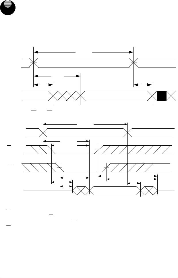
READ CYCLE 1 (Address Controlled) (1,2,4) |
|
|
tRC
Address
|
tAA |
tOH |
tOH |
DOUT |
Data Valid |
READ CYCLE 2 ( CE and OE Controlled) (1,3,5,6)
t RC
Address
|
|
t AA |
CE |
|
t ACE |
|
OE
|
|
|
|
|
|
t OE |
|
|
|
t CHZ |
|
|
|||
|
t |
|
|
|
|
|
t OHZ |
|
|
||||||
|
CLZ |
|
|
|
|||||||||||
|
|
|
|
|
|
|
|
|
|||||||
|
|
|
|
|
|
|
|
|
|
t OH |
|
|
|
|
|
Dout |
HIGH-Z |
t OLZ |
|
|
|
|
HIGH-Z |
||||||||
|
|
|
|
|
|||||||||||
|
|
|
|
|
|
|
|
|
|
|
|||||
|
|
|
|
|
|
|
|
|
Data Valid |
||||||
Notes :
1.WE is HIGH for read cycle.
2.Device is continuously selected CE =VIL.
3. Address must be valid prior to or coincident with CE transition; otherwise tAA is the limiting parameter.
4.OE is LOW.
5.tCLZ, tOLZ, tCHZ and tOHZ are specified with CL = 5pF. Transition is measured ±500mV from steady state.
6.At any given temperature and voltage condition, tCHZ is less than tCLZ, tOHZ is less than tOLZ.
UTRON TECHNOLOGY INC. |
P80052 |
1F, No. 11, R&D Rd. II, Science-Based Industrial Park, Hsinchu, Taiwan, R. O. C. TEL: 886-3-5777882 FAX: 886-3-5777919
5
 Loading...