


UTRON UT51C164MC-60, UT51C164MC-50, UT51C164MC-40, UT51C164MC-35, UT51C164JC-60 Datasheet
...UTRON |
UT51C164 |
Rev 1.4 |
256K X 16 BIT EDO DRAM |
FEATURES |
|
RAS access time: 35, 40, 50, 60
2 CAS Byte/Word Read/Write operation CAS - before – RAS refresh capability RAS only and Hidden refresh capability
Early write or output enable controlled write Extended Data Out operation
Package : 40 pin 400mil SOJ
40 / 44 pin 400mil TSOPSingle +5V+10% power supply
TTL compatible inputs and outputs 512 refresh cycles /8ms
Speed |
-35 |
-40 |
-50 |
-60 |
tRAC |
35ns |
40ns |
50ns |
60ns |
tCAA |
18ns |
20ns |
24ns |
30ns |
tPC |
14ns |
15ns |
19ns |
27ns |
tCAC |
11ns |
12ns |
14ns |
15ns |
tRC |
70ns |
75ns |
90ns |
110ns |
GENERAL DESCRIPTION
The UT51C164 is high speed 5V EDO DRAMs organized as 256K bit X 16 I/O and fabricated with the CMOS process. The UT51C164 offers a combination of unique features including : EDO Page Mode operation for higher bandwidth with Page Mode cycle time as short as 14ns. All inputs are TTL compatible. Input and output capacitance is significantly lowered to increase performance and minimize loading. These features make the UT51C164 suited for wide variety of high performance computer systems and peripheral applications
UTRON TECHNOLOGY INC. |
P90005 |
1F, No. 11, R&D Rd. II, Science-Based Industrial Park, Hsinchu, Taiwan, R. O. C. TEL: 886-3-5777882 FAX: 886-3-5777919
1
|
|
|
|
|
|
|
UTRON |
|
UT51C164 |
||
Rev 1.4 |
|
|
256K X 16 BIT EDO DRAM |
||||||||
PIN DESCRIPTION |
|
|
|||||||||
|
|
|
|
|
|
|
|
|
|
|
|
SYMBOL |
|
DESCRIPTION |
|
|
|||||||
A0-A8 |
|
Address Inputs |
|
|
|||||||
|
|
|
|
|
|
|
|
|
Row Address Strobe |
|
|
|
RAS |
|
|
|
|||||||
|
|
|
|
|
|
|
|
|
Column Address Strobe / Upper Byte Control |
|
|
|
UCAS |
|
|
||||||||
|
|
|
|
|
|
|
|
Column Address Strobe / Lower Byte Control |
|
||
|
LCAS |
|
|
||||||||
|
|
|
|
|
|
Write enable |
|
|
|||
|
|
WE |
|
|
|
||||||
|
|
|
|
|
Output enable |
|
|
||||
|
OE |
|
|
|
|||||||
DQ0-DQ15 |
|
Data Inputs, Data Outputs |
|
|
|||||||
VDD |
|
+5V Supply |
|
|
|||||||
Vss |
|
0V Supply |
|
|
|||||||
NC |
|
No Connect |
|
|
|||||||
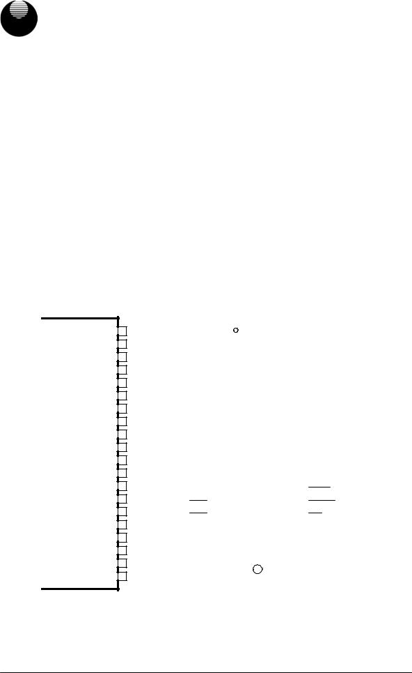
PIN CONFIGURATIONS |
|
|
|||||||||
|
|
|
|
|
|
|
|
UT51C164 |
UT51C164 |
||
|
|
|
|
|
|
|
|
40pin SOJ |
40pin TSOP - |
||
VDD |
|
|
1 |
40 |
|
|
|
||||
DQ0 |
|
|
2 |
39 |
|
DQ1 |
|
|
3 |
38 |
|
DQ2 |
|
4 |
37 |
||
DQ3 |
|
|
|
36 |
|
|
5 |
||||
VDD |
|
|
6 |
35 |
|
|
|
||||
DQ4 |
|
7 |
34 |
||
DQ5 |
|
|
|
33 |
|
|
|
8 |
|||
DQ6 |
|
9 |
32 |
||
DQ7 |
|
|
|
31 |
|
|
|
10 |
|||
NC |
|
11 |
30 |
||
NC |
|
|
|
29 |
|
|
12 |
||||
|
|
|
|
|
|
WE |
|
13 |
28 |
||
|
|
|
|
|
|
RAS |
|
|
14 |
27 |
|
NC |
|
15 |
26 |
||
A0 |
|
|
|
25 |
|
|
|
16 |
|||
A1 |
|
17 |
24 |
||
A2 |
|
|
|
23 |
|
|
|
18 |
|||
A3 |
|
19 |
22 |
||
VDD |
|
|
20 |
21 |
|
|
|
||||
|
|
|
|
|
|
|
|
Vss |
VDD |
|
1 |
40 |
|
||
|
|
|
|
||||||
|
|
DQ15 |
DQ0 |
|
2 |
39 |
|
||
|
|
||||||||
|
|
DQ14 |
DQ1 |
|
3 |
38 |
|
||
|
|
||||||||
|
|
DQ13 |
DQ2 |
|
4 |
37 |
|
||
|
|
||||||||
|
|
|
|
|
DQ3 |
|
|
36 |
|
|
|
|
|
|
|
||||
|
|
DQ12 |
|
5 |
|
||||
|
|
|
|
|
VDD |
|
|
35 |
|
|
|
|
|
|
|
|
|
||
|
|
Vss |
|
6 |
|
||||
|
|
|
|
|
|
||||
|
|
|
|
||||||
|
|
DQ11 |
DQ4 |
|
7 |
34 |
|
||
|
|
DQ10 |
DQ5 |
|
|
33 |
|
||
|
|
|
|
|
|||||
|
|
|
|
|
DQ6 |
|
8 |
|
|
|
|
DQ9 |
|
|
32 |
|
|||
|
|
|
|
|
|||||
|
|
|
|
|
DQ7 |
|
9 |
|
|
|
|
DQ8 |
|
|
31 |
|
|||
|
|
|
|
|
|||||
|
|
NC |
|
|
10 |
|
|||
|
|
|
|
|
|
|
|||
|
|
|
|
|
|
|
|||
|
|
|
|
|
|
||||
|
|
|
|
|
|
|
|
|
|
|
|
LCAS |
NC |
|
11 |
30 |
|
||
|
|
|
|
|
|||||
|
|
UCAS |
|
|
|||||
|
|
NC |
|
12 |
29 |
|
|||
|
|
|
|
|
|
|
|||
|
|
|
|
|
|
||||
|
|
OE |
|
||||||
|
|
|
|
||||||
|
|
A8 |
WE |
|
13 |
28 |
|
||
|
|
|
|||||||
|
|
RAS |
|
14 |
27 |
|
|||
|
|
|
|||||||
|
|
A7 |
|
|
|||||
|
|
|
|||||||
|
|
|
|
|
|
||||
|
|
A6 |
NC |
|
15 |
26 |
|
||
|
|
|
|||||||
|
|
A0 |
|
16 |
25 |
|
|||
|
|
A5 |
|
|
|||||
|
|
|
|||||||
|
|
|
|||||||
|
|
|
|
|
|
||||
|
|
A4 |
A1 |
|
17 |
24 |
|
||
|
|
|
|||||||
|
|
|
|
|
|
||||
|
|
A2 |
|
|
23 |
|
|||
|
|
Vss |
|
18 |
|
||||
|
|
|
|||||||
|
|
|
|
|
|
||||
|
|
A3 |
|
19 |
22 |
|
|||
|
|
|
|
|
|
|
|||
|
|
|
|
|
|
|
|
|
|
|
|
|
|
|
VDD |
|
|
21 |
|
|
|
|
|
|
|
20 |
|
||
|
|
|
|
|
|
|
|
|
|
|
|
|
|
|
|
|
|
|
|
Vss
DQ15
DQ14
DQ13
DQ12
Vss
DQ11
DQ10
DQ9
DQ8
NC LCAS UCAS OE A8 A7 A6 A5 A4 Vss
UTRON TECHNOLOGY INC. |
P90005 |
1F, No. 11, R&D Rd. II, Science-Based Industrial Park, Hsinchu, Taiwan, R. O. C. TEL: 886-3-5777882 FAX: 886-3-5777919
2

UTRON |
|
|
|
|
|
|
|
|
UT51C164 |
|
Rev 1.4 |
|
|
|
256K X 16 BIT EDO DRAM |
||||||
FUNCTION BLOCK DIAGRAM |
|
|
|
|
|
|
|
|
V |
V |
|
|
WE |
|
UCAS |
|
LCAS |
|
RAS |
||
|
|
|
|
|
||||||
A0 A1 . . A7 A8 |
OE |
|
|
|
SS |
DD |
||||
. . |
|
|
|
|
|
|
|
|
|
|
|
|
|
|
|
|
|
|
|
|
|
Address Buffers
& Predecoders
Y8 – Y0
Decoder Column |
CS X512 |
|
|
9 |
Refresh Counter |
Control Circuit |
|
|
|
|
X0 |
|
|
– |
|
|
X8 |
|
Row Control Circuit
Row Decoder
Array Cell 16 x 512 x 512 Amp Sense
x16
FSA & Write in Circuit
x16
Input & Output Buffer
x16 DQ[0,15]
BBV
GENERATOR
BBV
UTRON TECHNOLOGY INC. |
P90005 |
1F, No. 11, R&D Rd. II, Science-Based Industrial Park, Hsinchu, Taiwan, R. O. C. TEL: 886-3-5777882 FAX: 886-3-5777919
3

|
UTRON |
|
|
UT51C164 |
|
|
Rev 1.4 |
|
256K X 16 BIT EDO DRAM |
||
|
ABSOLUTE MAXIMUM RATINGS |
|
|
|
|
|
PARAMETER |
SYMBOL |
VALUE |
UNIT |
|
|
Voltage on any pin relative to Vss |
VT |
-1.0 to +7 |
V |
|
|
Supply voltage relative to VSS |
VDD |
-1.0 to +7 |
V |
|
|
Short circuit output current |
IOUT |
50 |
mA |
|
|
Power dissipation |
PD |
1.0 |
W |
|
|
Operating temperature |
TA |
0 to + 70 |
ºC |
|
|
Storage temperature |
TSTG |
-55 to +125 |
ºC |
|
Notes: Permanent device damage may occur if absolute maximum ratings are exceed.
RECOMMENDED DC OPERATING CONDITIONS (TA = 0 to 70ºC)
PARAMETER |
SYMBOL |
|
5.0V |
UNIT |
NOTES |
|
MIN |
|
MAX |
||||
|
|
|
|
|
||
Supply voltage |
VDD |
4.5 |
|
5.5 |
V |
1 |
Vss |
0 |
|
0 |
V |
- |
|
|
|
|||||
Input high voltage |
VIH |
2.4 |
|
VDD +1V |
V |
1 |
Input low voltage |
VIL |
-0.3 |
|
0.8 |
V |
1 |
Notes: 1. All Voltage referred to Vss
CAPACITANCE (TA = 25ºC, VDD= 5V±0.5V f=1MHz)
|
|
|
PARAMETER |
SYMBOL |
TYP |
MAX |
UNIT |
|||||||
Input capacitance (A0-A8) |
CIN1 |
3 |
4 |
pF |
||||||||||
Input Capacitance |
CIN2 |
4 |
5 |
pF |
||||||||||
( |
RAS |
, |
UCAS |
, |
LCAS |
, |
WE |
, |
OE |
) |
|
|
|
|
Output capacitance(DQ0-DQ15) |
CDQ |
5 |
7 |
pF |
||||||||||
UTRON TECHNOLOGY INC. |
P90005 |
1F, No. 11, R&D Rd. II, Science-Based Industrial Park, Hsinchu, Taiwan, R. O. C. TEL: 886-3-5777882 FAX: 886-3-5777919
4

|
|
UTRON |
|
|
|
|
|
UT51C164 |
|||||||||||
Rev 1.4 |
|
|
|
|
|
|
|
256K X 16 BIT EDO DRAM |
|||||||||||
DC CHARACTERISTICS (TA = 0 to 70ºC, VDD = 5.0 V ± 0.5 V, Vss = 0 V) |
|||||||||||||||||||
|
|
|
|
|
|
|
|
|
|
|
|
|
|
|
|
|
|
|
|
SYMBOL |
PARAMETER |
|
SPEED |
UT51C164 |
UNIT |
TEST CONDITION |
|||||||||||||
|
(tRAC) |
Min |
Max |
||||||||||||||||
|
|
|
|
|
|
|
|
|
|
|
|
|
|
|
|
||||
|
Operating Current, |
-35 |
- |
190 |
|
|
|
|
|
|
|
|
|
|
|||||
IDD1 |
-40 |
- |
180 |
mA |
tRC = tRC (min.) |
||||||||||||||
VDD Supply |
|
-50 |
- |
170 |
|||||||||||||||
|
|
|
|
|
|
|
|
|
|
|
|
||||||||
|
|
|
|
|
|
-60 |
- |
160 |
|
|
|
|
|
|
|
|
|
|
|
|
Standby Current |
|
|
|
|
|
|
= |
|
|
= |
|
|
||||||
IDD2 |
- |
- |
3 |
mA |
RAS |
UCAS |
LCAS |
||||||||||||
|
(TTL Input) |
|
=VIH |
||||||||||||||||
|
|
|
|
|
|
|
|||||||||||||
|
|
|
|
Only |
Refresh |
-35 |
- |
190 |
|
|
|
|
|
|
|
|
|
|
|
IDD3 |
|
RAS |
|
-40 |
- |
180 |
mA |
tRC = tRC (min.) |
|||||||||||
Current |
|
-50 |
- |
170 |
|||||||||||||||
|
|
|
|
|
|
|
|
|
|
|
|
||||||||
|
|
|
|
|
|
-60 |
- |
160 |
|
|
|
|
|
|
|
|
|
|
|
|
EDO |
Page |
Mode |
-35 |
- |
220 |
|
|
|
|
|
|
|
|
|
|
|||
IDD4 |
-40 |
- |
200 |
mA |
tPC = tPC (min.) |
||||||||||||||
Current |
|
-50 |
- |
190 |
|||||||||||||||
|
|
|
|
|
|
|
|
|
|
|
|
||||||||
|
|
|
|
|
|
-60 |
- |
180 |
|
|
|
|
|
|
|
|
|
|
|
|
|
|
|
|
|
-35 |
- |
190 |
|
|
|
|
|
|
|
|
|
|
|
IDD5 |
CBR Refresh Current |
-40 |
- |
180 |
mA |
tRC = tRC (min.) |
|||||||||||||
-50 |
- |
170 |
|||||||||||||||||
|
|
|
|
|
|
|
|
|
|
|
|
|
|
|
|
||||
|
|
|
|
|
|
-60 |
- |
160 |
|
|
|
|
|
|
|
|
|
|
|
|
|
|
|
|
|
|
|
|
|
|
|
|
VDD-0.2V |
||||||
IDD6 |
Standby Current |
- |
- |
2 |
mA |
RAS |
|||||||||||||
CAS VDD-0.2V |
|||||||||||||||||||
(CMOS Input) |
|
||||||||||||||||||
|
|
|
|
|
|
All other inputs VSS |
|||||||||||||
|
|
|
|
|
|
|
|
|
|
||||||||||
VDD |
Power Supply |
|
- |
4.5 |
5.5 |
V |
|
|
|
|
|
|
|
|
|
||||
ILI |
Input Leakage Current |
- |
-10 |
10 |
uA |
VSS VIN VDD |
|||||||||||||
ILO |
Output |
|
Leakage |
- |
-10 |
10 |
uA |
VSS VOUT VDD |
|||||||||||
Current |
|
|
|
|
|
|
|
|
|
|
|||||||||
|
RAS = CAS = VIH |
||||||||||||||||||
|
|
|
|
|
|
||||||||||||||
VIL |
Input Low Voltage |
- |
-1 |
0.8 |
V |
|
|
|
|
|
|
|
|
|
|||||
VIH |
Input High Voltage |
- |
2.4 |
VDD +1 |
V |
|
|
|
|
|
|
|
|
|
|||||
VOL |
Output Low Voltage |
- |
- |
0.4 |
V |
IOI = 2mA |
|||||||||||||
VOH |
Output High Voltage |
- |
2.4 |
- |
V |
IOH = 2mA |
|||||||||||||
Notes: IDD1, IDD3, IDD4, IDD5 are dependent on output loading and cycle rates. Specified values are obtained with the output open. IDD is specified as an average current. In IDD1, IDD3, and IDD5 address can be changed maximum once while
RAS =VIL. In IDD4, address can be changed maximum once within one EDO page cycle time, tPC.
UTRON TECHNOLOGY INC. |
P90005 |
1F, No. 11, R&D Rd. II, Science-Based Industrial Park, Hsinchu, Taiwan, R. O. C. TEL: 886-3-5777882 FAX: 886-3-5777919
5

|
|
UTRON |
|
|
|
|
|
|
|
|
|
UT51C164 |
|||||||||||||||||||||||||||||||
Rev 1.4 |
|
|
|
|
|
|
|
|
|
|
|
|
|
|
|
|
|
|
|
|
|
|
|
|
|
|
|
|
|
|
|
|
|
|
256K X 16 BIT EDO DRAM |
||||||||
AC CHARACTERISTICS (TA = 0 to 70°C) |
|
|
|
|
|
|
|
|
|
|
|
||||||||||||||||||||||||||||||||
Test condition: VDD = 5.0V±0.5V, VIH / VIL=3V / 0V, VOH / VOL=2.0 / 0.8) |
|
|
|
|
|
||||||||||||||||||||||||||||||||||||||
|
|
|
|
|
|
|
|
|
|
|
|
|
|
|
|
|
|
|
|
|
|
|
|
|
|
|
|
|
|
|
|
|
|
|
|
|
|
|
|
|
|
|
|
|
SYMBOL |
PARAMETER |
|
35 |
|
40 |
|
50 |
|
60 |
UNIT |
NOTE |
|||||||||||||||||||||||||||||||
|
Min. |
Max. |
Min. |
Max. |
Min. |
Max. |
Min. |
Max. |
|||||||||||||||||||||||||||||||||||
1 |
tRAS |
|
|
|
|
|
|
|
|
|
|
Pulse Width |
35 |
|
75K |
40 |
|
75K |
50 |
|
75K |
60 |
|
75K |
ns |
|
|||||||||||||||||
|
RAS |
|
|
|
|
|
|||||||||||||||||||||||||||||||||||||
2 |
tRC |
|
Read or Write Cycle Time |
70 |
|
|
75 |
|
|
90 |
|
|
110 |
|
|
ns |
|
||||||||||||||||||||||||||
3 |
tRP |
|
|
|
|
|
|
|
|
|
|
Precharge Time |
25 |
|
|
25 |
|
|
30 |
|
|
40 |
|
|
ns |
|
|||||||||||||||||
|
|
RAS |
|
|
|
|
|
|
|
|
|
||||||||||||||||||||||||||||||||
4 |
tCSH |
|
|
|
|
|
|
|
|
|
|
Hold Time |
35 |
|
|
40 |
|
|
50 |
|
|
60 |
|
|
ns |
|
|||||||||||||||||
|
|
|
CAS |
|
|
|
|
|
|
|
|
|
|||||||||||||||||||||||||||||||
5 |
tCAS |
|
|
|
|
|
|
|
|
|
|
Pulse Width |
8 |
|
|
8 |
|
|
10 |
|
|
10 |
|
|
ns |
|
|||||||||||||||||
|
|
|
CAS |
|
|
|
|
|
|
|
|
|
|||||||||||||||||||||||||||||||
6 |
tRCD |
|
|
|
|
|
|
|
|
|
|
to |
|
|
|
|
|
|
Delay |
13 |
|
24 |
17 |
|
28 |
19 |
|
36 |
20 |
|
45 |
ns |
|
||||||||||
|
|
RAS |
CAS |
|
|
|
|
|
|||||||||||||||||||||||||||||||||||
7 |
tRCS |
|
Read Command Setup Time |
0 |
|
|
0 |
|
|
0 |
|
|
0 |
|
|
ns |
*1 |
||||||||||||||||||||||||||
8 |
tASR |
|
Row Address Setup Time |
0 |
|
|
0 |
|
|
0 |
|
|
0 |
|
|
ns |
|
||||||||||||||||||||||||||
9 |
tRAH |
|
Row Address Hold Time |
6 |
|
|
7 |
|
|
9 |
|
|
10 |
|
|
ns |
|
||||||||||||||||||||||||||
10 |
tASC |
|
Column Address Setup Time |
0 |
|
|
0 |
|
|
0 |
|
|
0 |
|
|
ns |
|
||||||||||||||||||||||||||
11 |
tCAH |
|
Column Address Hold Time |
6 |
|
|
7 |
|
|
9 |
|
|
10 |
|
|
ns |
|
||||||||||||||||||||||||||
12 |
tRSH |
|
|
|
|
|
|
|
|
|
|
to |
|
|
|
|
|
|
Hold Time |
10 |
|
|
12 |
|
|
14 |
|
|
15 |
|
|
ns |
|
||||||||||
|
|
RAS |
CAS |
|
|
|
|
|
|
|
|
|
|||||||||||||||||||||||||||||||
|
|
|
|
|
|
|
|
|
|
|
|
to |
|
|
|
|
|
Precharge |
|
|
|
|
|
|
|
|
|
|
|
|
|
|
|||||||||||
13 |
tCRP |
|
|
|
CAS |
RAS |
5 |
|
|
5 |
|
|
5 |
|
|
5 |
|
|
ns |
|
|||||||||||||||||||||||
|
Time |
|
|
|
|
|
|
|
|
|
|||||||||||||||||||||||||||||||||
|
|
|
|
|
|
|
|
|
|
|
|
|
|
|
|
|
|||||||||||||||||||||||||||
14 |
tRCH |
|
Read Command Hold Time |
0 |
|
|
0 |
|
|
0 |
|
|
0 |
|
|
ns |
*2 |
||||||||||||||||||||||||||
|
|
|
|
|
|
|
|
|
|
|
|
|
|
|
|
|
|
|
|
|
|
|
|
|
|
|
|
|
|
|
|
|
|
|
|
||||||||
|
Reference CAS |
|
|
|
|
|
|
|
|
||||||||||||||||||||||||||||||||||
|
|
|
|
|
|
|
|
|
|
|
|
|
|
|
|
|
|||||||||||||||||||||||||||
15 |
tRRH |
|
Read Command Hold Time |
0 |
|
|
0 |
|
|
0 |
|
|
0 |
|
|
ns |
*2 |
||||||||||||||||||||||||||
|
|
|
|
|
|
|
|
|
|
|
|
|
|
|
|
|
|
|
|
|
|
|
|
|
|
|
|
|
|
|
|
|
|
|
|
||||||||
|
Reference RAS |
|
|
|
|
|
|
|
|
||||||||||||||||||||||||||||||||||
|
|
|
|
|
|
|
|
|
|
|
|
|
|
|
|
|
|||||||||||||||||||||||||||
|
|
|
|
|
|
|
|
|
|
|
|
Hold Time Referenced |
|
|
|
|
|
|
|
|
|
|
|
|
|
|
|||||||||||||||||
16 |
tROH |
|
|
RAS |
7 |
|
|
8 |
|
|
10 |
|
|
10 |
|
|
ns |
|
|||||||||||||||||||||||||
|
|
|
|
|
|
|
|
|
|
|
|
|
|
|
|
|
|
|
|
|
|
|
|
|
|
|
|
|
|
|
|
|
|
|
|
|
|||||||
|
to OE |
|
|
|
|
|
|
|
|
|
|||||||||||||||||||||||||||||||||
|
|
|
|
|
|
|
|
|
|
|
|
|
|
|
|
|
|||||||||||||||||||||||||||
17 |
tOAC |
|
Access Time from |
|
|
|
|
|
|
|
|
11 |
|
|
12 |
|
|
14 |
|
|
15 |
ns |
*9 |
||||||||||||||||||||
|
OE |
|
|
|
|
|
|
|
|
||||||||||||||||||||||||||||||||||
18 |
tCAC |
|
Access Time from |
|
|
|
|
|
|
|
|
|
11 |
|
|
12 |
|
|
14 |
|
|
15 |
ns |
*3,4,11 |
|||||||||||||||||||
|
CAS |
|
|
|
|
|
|
|
|
||||||||||||||||||||||||||||||||||
19 |
tRAC |
|
Access Time from |
|
|
|
|
|
|
|
|
|
35 |
|
|
40 |
|
|
50 |
|
|
60 |
ns |
*3,5,6 |
|||||||||||||||||||
|
RAS |
|
|
|
|
|
|
|
|
||||||||||||||||||||||||||||||||||
20 |
tCAA |
|
Access Time From Column |
|
|
18 |
|
|
20 |
|
|
24 |
|
|
30 |
ns |
*3,4,7 |
||||||||||||||||||||||||||
|
Address |
|
|
|
|
|
|
|
|
||||||||||||||||||||||||||||||||||
|
|
|
|
|
|
|
|
|
|
|
|
|
|
|
|
|
|||||||||||||||||||||||||||
21 |
tLZ |
|
|
|
|
|
|
or |
|
|
|
|
|
to Low-Z Output |
0 |
|
|
0 |
|
|
0 |
|
|
0 |
|
|
ns |
*13 |
|||||||||||||||
|
|
|
OE |
CAS |
|
|
|
|
|
|
|
|
|||||||||||||||||||||||||||||||
|
|
|
|
|
|
|
|
or |
|
|
|
|
|
to High-Z |
|
|
|
|
|
|
|
|
|
|
|
|
|
|
|||||||||||||||
22 |
tHZ |
|
|
|
OE |
CAS |
0 |
|
5 |
0 |
|
6 |
0 |
|
8 |
0 |
|
10 |
ns |
*13 |
|||||||||||||||||||||||
|
Output |
|
|
|
|
||||||||||||||||||||||||||||||||||||||
|
|
|
|
|
|
|
|
|
|
|
|
|
|
|
|
|
|||||||||||||||||||||||||||
23 |
tAR |
|
Column Address Hold Time |
25 |
|
|
30 |
|
|
40 |
|
|
50 |
|
|
ns |
|
||||||||||||||||||||||||||
|
|
|
|
|
|
|
|
|
|
|
|
|
|
|
|
|
|
|
|
|
|
|
|
|
|
|
|
|
|
|
|
|
|
|
|
|
|||||||
|
from RAS |
|
|
|
|
|
|
|
|
|
|||||||||||||||||||||||||||||||||
|
|
|
|
|
|
|
|
|
|
|
|
|
|
|
|
|
|||||||||||||||||||||||||||
|
|
|
|
|
|
|
|
|
to Column Address |
|
|
|
|
|
|
|
|
|
|
|
|
|
|
||||||||||||||||||||
24 |
tRAD |
|
|
RAS |
10 |
|
17 |
12 |
|
20 |
14 |
|
26 |
15 |
|
30 |
ns |
*8 |
|||||||||||||||||||||||||
|
Delay Time |
|
|
|
|
||||||||||||||||||||||||||||||||||||||
|
|
|
|
|
|
|
|
|
|
|
|
|
|
|
|
|
|||||||||||||||||||||||||||
25 |
tT |
|
Transition Time |
1.5 |
|
50 |
1.5 |
|
50 |
1.5 |
|
50 |
1.5 |
|
50 |
ns |
*12 |
||||||||||||||||||||||||||
|
|
|
Write Command to |
|
|
|
|
|
|
|
|
|
|
|
|
|
|
|
|
|
|
|
|||||||||||||||||||||
26 |
tCWL |
|
CAS |
8 |
|
|
10 |
|
|
10 |
|
|
10 |
|
|
ns |
|
||||||||||||||||||||||||||
|
Lead Time |
|
|
|
|
|
|
|
|
|
|||||||||||||||||||||||||||||||||
|
|
|
|
|
|
|
|
|
|
|
|
|
|
|
|
|
|||||||||||||||||||||||||||
27 |
tWCS |
|
Write Command Setup Time |
0 |
|
|
0 |
|
|
0 |
|
|
0 |
|
|
ns |
*9,10 |
||||||||||||||||||||||||||
28 |
tWCH |
|
Write Command Hold time |
5 |
|
|
6 |
|
|
7 |
|
|
10 |
|
|
ns |
|
||||||||||||||||||||||||||
29 |
tWP |
|
Write Pulse Width |
5 |
|
|
6 |
|
|
7 |
|
|
10 |
|
|
ns |
|
||||||||||||||||||||||||||
UTRON TECHNOLOGY INC. |
P90005 |
1F, No. 11, R&D Rd. II, Science-Based Industrial Park, Hsinchu, Taiwan, R. O. C. TEL: 886-3-5777882 FAX: 886-3-5777919
6

|
|
UTRON |
|
|
|
|
|
|
|
UT51C164 |
|||||||||||||||||||||||||||||
Rev 1.4 |
|
|
|
|
|
|
|
|
|
|
|
|
|
|
|
|
|
|
|
|
|
|
|
|
|
|
|
|
|
|
|
256K X 16 BIT EDO DRAM |
|||||||
AC CHARACTERISTICS ( continued ) |
|
|
|
|
|
|
|
|
|
||||||||||||||||||||||||||||||
|
|
|
|
|
|
|
|
|
|
|
|
|
|
|
|
|
|
|
|
|
|
|
|
|
|
|
|
|
|
|
|
|
|
|
|
|
|
|
|
|
SYMBOL |
PARAMETER |
35 |
40 |
|
50 |
60 |
UNIT |
NOTE |
||||||||||||||||||||||||||||||
|
Min. |
Max. |
Min. |
Max. |
Min. |
Max. |
Min. |
Max. |
|||||||||||||||||||||||||||||||
30 |
tWCR |
|
Write Command Hold Time |
25 |
|
30 |
|
|
40 |
|
50 |
|
ns |
|
|||||||||||||||||||||||||
|
|
|
|
|
|
|
|
|
|
|
|
|
|
|
|
|
|
|
|
|
|
|
|
|
|
|
|
|
|
|
|
|
|||||||
|
from RAS |
|
|
|
|
|
|
||||||||||||||||||||||||||||||||
|
|
|
|
|
|
|
|
|
|
|
|
|
|
||||||||||||||||||||||||||
|
|
|
Write Command to |
|
|
|
|
|
|
|
|
|
|
|
|
|
|
|
|
|
|
||||||||||||||||||
31 |
tRWL |
|
RAS |
11 |
|
12 |
|
|
14 |
|
15 |
|
ns |
|
|||||||||||||||||||||||||
|
Lead Time |
|
|
|
|
|
|
||||||||||||||||||||||||||||||||
|
|
|
|
|
|
|
|
|
|
|
|
|
|
||||||||||||||||||||||||||
32 |
tDS |
|
Data in Setup Time |
0 |
|
0 |
|
|
0 |
|
0 |
|
ns |
*11 |
|||||||||||||||||||||||||
33 |
tDH |
|
Data in Hold Time |
5 |
|
6 |
|
|
7 |
|
10 |
|
ns |
*11 |
|||||||||||||||||||||||||
34 |
tWOH |
|
Write to |
|
|
|
|
Hold time |
5 |
|
6 |
|
|
8 |
|
10 |
|
ns |
*11 |
||||||||||||||||||||
|
OE |
|
|
|
|
|
|||||||||||||||||||||||||||||||||
35 |
tOED |
|
|
|
|
|
|
to Data Delay Time |
5 |
|
6 |
|
|
8 |
|
10 |
|
ns |
*11 |
||||||||||||||||||||
|
OE |
|
|
|
|
|
|||||||||||||||||||||||||||||||||
36 |
tRWC |
|
Read-Modify-Write Cycle Time |
105 |
|
110 |
|
|
130 |
|
170 |
|
ns |
|
|||||||||||||||||||||||||
37 |
tRRW |
|
Read-Modify-Write Cycle Time |
70 |
|
75 |
|
|
85 |
|
105 |
|
ns |
|
|||||||||||||||||||||||||
|
|
|
|
|
|
|
|
|
|
|
|
|
|
|
|
|
|
|
|
|
|
|
|
|
|
|
|
|
|
|
|
|
|||||||
|
|
RAS Pulse Width |
|
|
|
|
|
|
|||||||||||||||||||||||||||||||
|
|
|
|
|
|
|
|
|
|
|
|
|
|
|
|||||||||||||||||||||||||
|
|
|
|
|
|
|
|
|
|
|
to |
|
|
|
|
|
Delay in Read- |
|
|
|
|
|
|
|
|
|
|
|
|||||||||||
38 |
tCWD |
|
|
CAS |
WE |
28 |
|
30 |
|
|
34 |
|
40 |
|
ns |
*9 |
|||||||||||||||||||||||
|
Modify-Write Cycle |
|
|
|
|
|
|||||||||||||||||||||||||||||||||
|
|
|
|
|
|
|
|
|
|
|
|
|
|
||||||||||||||||||||||||||
|
|
|
|
|
|
|
|
|
|
|
to |
|
|
|
|
|
Delay in Read- |
|
|
|
|
|
|
|
|
|
|
|
|||||||||||
39 |
tRWD |
|
|
RAS |
WE |
54 |
|
58 |
|
|
68 |
|
85 |
|
ns |
*9 |
|||||||||||||||||||||||
|
Modify-Write Cycle |
|
|
|
|
|
|||||||||||||||||||||||||||||||||
|
|
|
|
|
|
|
|
|
|
|
|
|
|
||||||||||||||||||||||||||
40 |
tCRW |
|
|
|
|
|
|
|
|
|
pulse Width in RMW |
46 |
|
48 |
|
|
52 |
|
65 |
|
ns |
|
|||||||||||||||||
|
|
CAS |
|
|
|
|
|
|
|||||||||||||||||||||||||||||||
|
|
|
Column Address to |
|
|
|
Delay |
|
|
|
|
|
|
|
|
|
|
|
|||||||||||||||||||||
41 |
tAWD |
|
WE |
35 |
|
38 |
|
|
42 |
|
58 |
|
ns |
*9 |
|||||||||||||||||||||||||
|
Time |
|
|
|
|
|
|||||||||||||||||||||||||||||||||
|
|
|
|
|
|
|
|
|
|
|
|
|
|
||||||||||||||||||||||||||
42 |
tPC |
|
EDO Page Mode Read or |
14 |
|
15 |
|
|
19 |
|
27 |
|
ns |
|
|||||||||||||||||||||||||
|
Write Cycle Time |
|
|
|
|
|
|
||||||||||||||||||||||||||||||||
|
|
|
|
|
|
|
|
|
|
|
|
|
|
||||||||||||||||||||||||||
43 |
tCP |
|
|
|
|
|
|
|
Precharge Time |
4 |
|
5 |
|
|
7 |
|
10 |
|
ns |
|
|||||||||||||||||||
|
|
CAS |
|
|
|
|
|
|
|||||||||||||||||||||||||||||||
44 |
tCAR |
|
Column Address to |
18 |
|
20 |
|
|
24 |
|
30 |
|
ns |
|
|||||||||||||||||||||||||
|
|
|
|
|
|
|
|
|
|
|
|
|
|
|
|
|
|
|
|
|
|
|
|
|
|
|
|
|
|
|
|
|
|||||||
|
|
RAS Setup Time |
|
|
|
|
|
|
|||||||||||||||||||||||||||||||
|
|
|
|
|
|
|
|
|
|
|
|
|
|
|
|||||||||||||||||||||||||
45 |
tCAP |
|
Access Time from Column |
|
20 |
|
23 |
|
|
27 |
|
34 |
ns |
*4 |
|||||||||||||||||||||||||
|
Precharge |
|
|
|
|
|
|||||||||||||||||||||||||||||||||
|
|
|
|
|
|
|
|
|
|
|
|
|
|
||||||||||||||||||||||||||
46 |
tDHR |
|
Data in Hold Time Referenced |
25 |
|
30 |
|
|
40 |
|
50 |
|
ns |
|
|||||||||||||||||||||||||
|
|
|
|
|
|
|
|
|
|
|
|
|
|
|
|
|
|
|
|
|
|
|
|
|
|
|
|
|
|
|
|
|
|||||||
|
to RAS |
|
|
|
|
|
|
||||||||||||||||||||||||||||||||
|
|
|
|
|
|
|
|
|
|
|
|
|
|
||||||||||||||||||||||||||
|
|
|
|
|
|
|
|
|
|
|
Setup Time in CBR |
|
|
|
|
|
|
|
|
|
|
|
|||||||||||||||||
47 |
tCSR |
|
|
CAS |
8 |
|
10 |
|
|
10 |
|
10 |
|
ns |
|
||||||||||||||||||||||||
|
Refresh |
|
|
|
|
|
|
||||||||||||||||||||||||||||||||
|
|
|
|
|
|
|
|
|
|
|
|
|
|
||||||||||||||||||||||||||
|
|
|
|
|
|
|
|
|
|
to |
|
|
|
|
|
Precharge |
|
|
|
|
|
|
|
|
|
|
|
||||||||||||
48 |
tRPC |
|
|
RAS |
CAS |
0 |
|
0 |
|
|
0 |
|
0 |
|
ns |
|
|||||||||||||||||||||||
|
Time |
|
|
|
|
|
|
||||||||||||||||||||||||||||||||
|
|
|
|
|
|
|
|
|
|
|
|
|
|
||||||||||||||||||||||||||
|
|
|
|
|
|
|
|
|
Hold Time in CBR |
|
|
|
|
|
|
|
|
|
|
|
|||||||||||||||||||
49 |
tCHR |
|
|
CAS |
8 |
|
9 |
|
|
12 |
|
15 |
|
ns |
|
||||||||||||||||||||||||
|
Refresh |
|
|
|
|
|
|
||||||||||||||||||||||||||||||||
|
|
|
|
|
|
|
|
|
|
|
|
|
|
||||||||||||||||||||||||||
50 |
tPCM |
|
EDO Page Mode Cycle Time |
55 |
|
60 |
|
|
70 |
|
85 |
|
ns |
|
|||||||||||||||||||||||||
|
in RMW |
|
|
|
|
|
|
||||||||||||||||||||||||||||||||
|
|
|
|
|
|
|
|
|
|
|
|
|
|
||||||||||||||||||||||||||
51 |
tCOH |
|
Output Hold After |
|
|
|
|
Low |
3 |
|
3 |
|
|
3 |
|
3 |
|
ns |
|
||||||||||||||||||||
|
CAS |
|
|
|
|
|
|
||||||||||||||||||||||||||||||||
|
|
|
|
|
|
|
|
Low to |
|
|
|
High Setup |
|
|
|
|
|
|
|
|
|
|
|
||||||||||||||||
52 |
tOES |
|
|
OE |
CAS |
3 |
|
4 |
|
|
6 |
|
8 |
|
ns |
|
|||||||||||||||||||||||
|
Time |
|
|
|
|
|
|
||||||||||||||||||||||||||||||||
|
|
|
|
|
|
|
|
|
|
|
|
|
|
||||||||||||||||||||||||||
|
|
|
|
|
|
|
|
Hold Time from |
|
|
|
|
in |
|
|
|
|
|
|
|
|
|
|
|
|||||||||||||||
53 |
tOEH |
|
|
OE |
WE |
5 |
|
6 |
|
|
8 |
|
10 |
|
ns |
|
|||||||||||||||||||||||
|
RMW Cycle |
|
|
|
|
|
|
||||||||||||||||||||||||||||||||
|
|
|
|
|
|
|
|
|
|
|
|
|
|
||||||||||||||||||||||||||
54 |
tOEP |
|
|
|
|
|
|
Pulse Width |
8 |
|
10 |
|
|
14 |
|
18 |
|
ns |
|
||||||||||||||||||||
|
|
OE |
|
|
|
|
|
|
|||||||||||||||||||||||||||||||
55 |
tREF |
|
Refresh Interval (512 Cycles) |
|
8 |
|
8 |
|
|
8 |
|
8 |
ms |
*14 |
|||||||||||||||||||||||||
UTRON TECHNOLOGY INC. |
P90005 |
1F, No. 11, R&D Rd. II, Science-Based Industrial Park, Hsinchu, Taiwan, R. O. C. TEL: 886-3-5777882 FAX: 886-3-5777919
7

UTRON |
UT51C164 |
Rev 1.4 |
256K X 16 BIT EDO DRAM |
Notes:
1. tRCD (Max.) is specified for reference only. Operation within tRCD (Max.) limits insures that tRAC (Max.) and tCAA (Max.) can be met. If tRCD is greater than the specified tRCD (Max.), the access time is controlled by tCAA and tCAC.
2.Either tRRH or tRCH must be satisfied for Read Cycle to occur.
3.Measured with a load equivalent to one TTL input and 50pF.
4.Access time is determined by the longest of tCAA , tCAC and tCAP .
5.Assumes that tRAD tRAD (Max.). If tRCD is greater than tRCD (Max.), tRAC will increase by the amount that tRCD exceeds tRCD (Max.)
6.Assumes that tRCD tRCD (Max.). If tRCD is greater than tRCD (Max.), tRAC will increase by the amount that tRAD exceeds tRAD (Max.)
7.Assumes that tRAD tRAD (Max.).
8.Operation within the tRAD (Max.) limits ensures that tRA can be met. tRAD (Max.) is specified as a reference point only. If tRAD is greater than the specified tRAD (Max.), the access time is controlled
by tCAA and tCAC.
9.tWCS , tRWD , tAWD and tCWD are not restrictive operating parameters.
10.tWCS (min.) must be satisfied in an Early Write Cycle.
11.tDS and tDH are referenced to the latter occurrence of CAS or WE .
12.tT is measured between VIH (min.) and VIL (max.). AC-measurements assume tT = 3ns.
13.Assumes a tri-state test load (5pF and a 500Ohm Thevenin equivalent).
14.An initial pause of 200us is required after power-up followed by any 8 CBR or ROR cycles before device operation is achieved.
UTRON TECHNOLOGY INC. |
P90005 |
1F, No. 11, R&D Rd. II, Science-Based Industrial Park, Hsinchu, Taiwan, R. O. C. TEL: 886-3-5777882 FAX: 886-3-5777919
8
 Loading...