


TM 11-6625-2759-14 & P
TECHNICAL MANUAL
OPERATOR’S, ORGANIZATIONAL, DIRECT
SUPPORT, AND GENERAL SUPPORT
MAINTENANCE MANUAL INCLUDING
REPAIR PARTS AND SPECIAL TOOLS LISTS
SPECTRUM ANALYZER PL-1391/U
(TEKTRONIX MODEL 7L5) (NSN 6625-01-015-6587)
HEADQUARTERS, DEPARTMENT OF THE ARMY
DECEMBER 1978
WARNING
DANGEROUS VOLTAGES
exist in this equipment. Be extremely careful when working on the power supply circuit or the AC line connections during line power operation. Serious injury or DEATH may result from contact with these points.
DON’T TAKE CHANCES!

TM 11-6625-2759-14 & P
This manual contains copywrite material reproduced by permission of the Tektronix Company.
TECHNICAL MANUAL HEADQUARTERS
DEPARTMENT OF THE ARMY
NO. 11-6625-2759-14 & P WASHINGTON, DC, 6December 1978
OPERATOR’S, ORGANIZATIONAL, DIRECT SUPPORT,
AND GENERAL SUPPORT MAINTENANCE MANUAL
INCLUDING REPAIR PARTS AND SPECIAL TOOLS LISTS
SPECTRUM ANALYZER PL-1391/U
(TEKTRONIX MODEL 7L5)
(NSN 6625-01-015-6587)
REPORTING OF ERRORS
You can improve this manual by recommending improvements using DA Form 2028-2 located in the back of the manual. Simply tear out the selfaddressed form, fill it out as shown on the sample, fold it where shown, and drop it in the mail.
If there are no blank DA Forms 2028-2 in the back of the manual, use the standard DA Form 2028 (Recommended Changes to Publications and Blank Forms) and forward to the Commander, US Army Communications and Electronics Materiel Readiness Command, ATTN: DRSEL-ME-MQ, Fort Monmouth, NJ 07703.
In either case a reply will be furnished direct to you.
NOTE
This manual is an authentication of the manufacturer’s commercial literature which, through usage, has been found to cover the data required to operate and maintain this equipment. Since the manual was not prepared in accordance with military specifications and AR 310-3, the format has not been structured to consider levels of maintenance.
i
PART I |
|
TM 11-6625-2759-14 & P |
|
TABLE OF CONTENTS |
|
|
|
PAGE |
Section 0 |
INTRODUCTION |
0-1 |
Section 1 |
General Information |
|
|
Introduction |
1-1 |
|
Description |
1-1 |
|
Specification |
1-1 |
|
Frequency Characteristics |
1-1 |
|
Input Characteristics |
1-2 |
|
Amplitude Characteristics |
1-2 |
|
Sweep Characteristics |
1-3 |
|
Output Connectors |
1-3 |
|
Environmental Characteristics |
1-4 |
|
Physical Characteristics |
1-4 |
|
Accessories and Options |
1-4 |
Section 2 |
Installation |
|
|
Initial Inspection |
2-1 |
|
Installation |
2-1 |
|
Repackaging |
2-1 |
Section 3 |
Operating Instructions |
|
|
Introduction |
3-1 |
|
Functional Block Description |
3-1 |
|
Front Panel Controls and Connectors |
3-3 |
|
Calibrating the 7L5 to the Oscilloscope Mainframe |
3-7 |
|
Operational Checkout |
3-8 |
|
Preliminary Preparation |
3-8 |
|
Operational Check of Readout Characters |
3-8 |
|
Dynamic Range Accuracy |
3-10 |
|
Reference Level Accuracy |
3-11 |
|
Input Buffer |
3-12 |
|
Residual (Incidental) FM |
3-12 |
|
Residual Response |
3-12 |
|
Sensitivity Check |
3-13 |
|
Resolution Bandwidth Accuracy, Amplitude Deviation and Shape Factor |
3-13 |
|
Using the Analyzer |
3-14 |
|
Impedance Matching |
3-14 |
|
Signal Application |
3-14 |
|
Edge Noise |
3-14 |
|
Frequency Measurement Technique |
3-15 |
|
Max Span Operation |
3-15 |
|
Resolution and Resolution Bandwidth |
3-15 |
|
Digital Storage |
3-15 |
|
Applications for Spectrum Analyzers |
3-15 |
TM 11-6625-2759-14 & P
SECTION 0
INTRODUCTION
0-1. SCOPE
This manual describes Spectrum Analyzer PL1391/U and provides instructions for operation (Part I) and maintenance (Part II). Throughout this manual the PL-1391/U is referred to as the Tekronix Model 7L5.
0-2. INDEXES OF PUBLICATIONS
a. DA Pam 310-4. Refer to the latest issue of DA Pam 310-4 to determine whether there are new editions, changes, or additional publications pertaining to the equipment.
b. DA Pam 310-7. Refer to the DA Pam 310-7 to determine whether there are modification work orders (MWO’s) pertaining to the equipment.
0-3. FORMS AND RECORDS
a.Reports of Maintenance and Unsatisfactory Equipment. Maintenance forms, records, and reports which are to be used by maintenance personnel at all maintenance levels are listed in and prescribed by TM 38-750.
b.Report of Packaging and Handling Deficiencies. Fill out and forward DD Form 6 (Packaging Improvement Report) as prescribed in AR 70058/NAVSUPINST 4030.29/AFR 71-13Imco P4030.29A and DLAR 4145.8.
c. Discrepancy in Shipment Report (DISREP) (SF 361). Fill out and forward Discrepancy in Shipment Report (DISREP) (SF 361) as prescribed in AR 5538/NAVSUPINST 4610.33B/AFR 75-18/MCO P4610.19C and DLAR 4500.15.
0-4. REPORTING EQUIPMENT IMPROVEMENT RECOMMENDATIONS (EIR)
EIR’s will be prepared using SF Form 368, Quality Deficiency Report. Instructions for preparing EIR’s are provided in TM 38-750, The Army Maintenance Management System. EIR’s should be mailed direct to Commander, US Army Communications and Electronics Materiel Readiness Command, ATTN: DRSEL-ME-MQ, Fort Monmouth, NJ 07703. A reply will be furnished direct to you.
0-5. ADMINISTRATIVE STORAGE
For information concerning storage, refer to section 2.
0-6. DESTRUCTION OF ARMY ELECTRONICS MATERIEL
Destruction of Army electronics materiel to prevent enemy use shall be in accordance with TM 750-244-2.
0-1
TM 11-6625-2759-14 & P
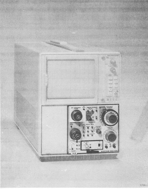
Fig. 1-1. 7L5 Spectrum Analyzer.
1-0
TM 11-6625-2759-14 & P
SECTION 1. SPECIFICATION
Introduction |
|
To effectively use the 7L5 Spectrum Analyzer, |
Frequency Characteristics |
|
|
the operation and capabilities of the instrument must be |
Range |
known This instruction manual covers general operating |
|
information about the instrument. Service information, |
Input Frequency: 10 Hz through 5 0 MHz. |
such as circuit description and calibration are contained |
|
in the Service manual. |
Dot Frequency: 0 Hz through 4999.75 kHz. |
Description |
Accuracy |
The 7L5 is a 5 MHz spectrum analyzer with |
20àC to 30°C: +(5 Hz + 2 x 10⁻⁶ of dot |
readout). |
|
digital storage. Frequency stability is within 5 Hz/hr and |
0°C to 50°C: ±(20 Hz + 10 -5 of dot |
center frequency (dot) can be read with six digit accuracy |
|
immediately after turn-on. There is no need to fine tune |
readout). |
the display Complex measurements and analysis can be |
|
made with relative ease. Built-in micro-processing |
Drift |
circuits decode control settings, process frequency and |
|
reference level information, and optimize sweep time and |
5 Hz/hour or less. |
resolution for the selected frequency span. |
|
The 7L5 with 80 dB or more of spurious free dynamic range, provides the ability to measure wide relative amplitudes. Nanovolt sensitivity provides very low-level signal and noise measurements.
The 7L5 display is fully calibrated in dBm, dBV, or volts/div The reference level can be accurately set to 1 dB increments. A front panel input buffer control increases front-end immunity to intermodulation distortion while maintaining a constant reference level. To accommodate a wide variety of impedance sources, the 7L5 uses quick disconnect plug-in input impedance modules of 50 Ò, 75 Ò, 600 Ò, 1 MÒ/28 pF and customized units to meet special requirements.
Digital storage allows any 7000-Series mainframe, with crt readout, to present clean, easy to photograph, displays. A smooth integrated display provides an accurate analysis of most displays. Two complete displays can be held in memory for comparison Two modes select either the conventional peak display or a digitally averaged display.
ELECTRICAL CHARACTERISTICS
The following electrical characteristics apply when the 7L5 Spectrum Analyzer, in combination with a Plug-In Module, are normally installed in a 7000-Series oscilloscope and after a warm-up of ten minutes or more.
Residual (Incidental) FM
50 Hz/div to 2 kHz/div: 1 Hz (p-p) or less.
5 kHz/div to 500 kHz/div. 40 Hz (p-p) or less.
Resolution Bandwidth
Accuracy
30 kHz--30 Hz: Within 20% of selected resolution (6 dB down).
10 Hz: Within 100 Hz ±20 Hz (70 dB down).
The COUPLED setting electronically selects the best resolution bandwidth for each setting of the FREQUENCY SPAN/DIV control.
Shape Factor
30 kHz-3 kHz 5:1 or better (60:6 dB ratio).
1 kHz-10 Hz: 10:1 or better (60:6 dB ratio).
Amplitude Deviation
30 kHz-100 Hz: 0.5 dB or less.
30 kHz-10 Hz: 2.0 dB or less.
1-1

Input Characteristics
CAUTION
The application of a dc voltage to the INPUT of the L1 or L2 Plug-In Modules may cause permanent damage to the mixer circuit.
Input Impedance (Nominal):
L1 50Ò
L2 75Ò
L3 Selectable (50Ò, 600Ò, and 1 MÒ/28 pF).
Input Power (maximum Input level for reference levels of 0 dBm or greater):
L1 21 dBm or 2.5 V rms
L2 21 dBm or 3.07 V rms
L3 21 dBm-input terminated 50Ò or 600Ò; 100 V (peak ac + dc) Input 1 MÒ/28 pF.
Input Power (maximum input level for reference levels below 0 dBm):
L1 +10 dBm
L2 +10 dBm
L3 +10 dBm--input terminated 50Ò or 600Ò, and 100 V (peak ac + dc) with input of 1 MÒ3/28 pF.
TM 11-6625-2759-14 & P
|
Equivalent Input Noise |
|||
Resolution |
(equal to or better than) |
|||
Bandwidth |
L1 |
L2 |
L3 |
|
|
|
|
|
|
10 Hz |
-135 dBm |
-135 dBm |
-148 dBV |
|
30 Hz |
-133 dBm |
-133 dBm |
-146 dBV |
|
100 Hz |
-130 dBm |
-130 dBm |
-143 dBV |
|
300 Hz |
-125 dBm |
-125 dBm |
-138 dBV |
|
1 kHz |
-120 dBm |
-120 dBm |
-133 dBV |
|
3 kHz |
-115 dBm |
-115 dBm |
-128 dBV |
|
10 kHz |
-110 dBm |
-110 dBm |
-123 dBV |
|
30 kHz |
-105 dBm |
-105 dBm |
-118 dBV |
|
|
|
|
|
|
NOTE
Sensitivity is degraded an additional 8 dB when the INPUT BUFFER is on; e.g., at 3 kHz, the equivalent input noise would be -107 dBm instead of -115 dBm. Noise level will increase by approximately 10 dB when operation Is In video peak mode,.
Intermodulation Distortion
Intermodulation products from two on-screen signals, within any frequency span are >75 dB down for third order products and at least 72 dB down for second order products.
Second and third order intermodulation products from two on-screen -53 dBV or less signals within any frequency span are at least 80 dB down.
Amplitude Characteristics
NOTE
If digital storage is used, an additional quantization error of 0.5% of full screen should be added to the amplitude characteristics.
Residual Response
Internally generated spurious signals are -130 dBm or less referred to the input (harmonics of the calibrator are -125 dB) with L1 or L2 plug-in module and - 143 dBV with the L3 plug-in module.
Sensitivity
The following tabulation of equivalent input noise for each resolution bandwidth is measured with; the INPUT BUFFER off, the VIDEO PEAK/AVG at max cw, and the TIME/DIV set to 10 seconds.
1-2
With the INPUT BUFFER switch on, the second and third order intermodulation products, for any two onscreen signals, within any frequency span, are at least 80 dB down.
Display Flatness
Peak to peak deviation, over any selected frequency span: Quantization error must be added (see Note under Amplitude Characteristics) if digital storage is used.
L1 0.5 dB;
L2 0.5 dB;
L3 0.5 dB
Reference Level
Refers to top graticule line in Log mode. Calibrated in 1 dB and 10 dB steps for the L1 and L2 modules and 1 dB/2 dB and 10 dB for L3 plug-in module.
Range |
|
L1 |
|
L2 |
|
L3 |
|
|
|
|
|
|
|
Log |
|
-128 dBm |
|
-128 dBm/ |
|
-128 dBm to |
2 dB/Div |
|
to +21 dBm |
|
139 dBV to |
|
+21 dBm (50Ò), |
|
|
|
|
+21 dBm/ |
|
-139 dBm to |
|
|
|
|
+10 dBV |
|
+10dBm (600Ò), |
|
|
|
|
|
|
-141 dBV to |
|
|
|
|
|
|
+8 dBV (Hi Z) |
Log |
|
-70 dBm |
|
-70 dBm/ |
|
-70 dBm to |
|
|
10 dB/Div |
|
-81 dBV to |
|
+21 dBm (50Ò), |
|
|
to +21 dBm |
|
|
|
|
|
|
|
|
+21 dBm/ |
|
-81 dBm to |
|
|
|
|
+10 dBV |
|
+10 dBm (600 Ò), |
-83 dBV to +8 dBV (Hi Z)
Incremental Accuracy
When calibrated at -40 dBV in Log mode.
L1, L2 and L3: Within 0.2 dB/dB with cumulative error of 0.25 dB/10 dB.
Lin Mode Range: 20 nV/Div to 200 mV/Div within 5% in 1-2-5 sequence.
NOTE
A >sign is displayed adjacent to the reference level readout when the reference level is not calibrated due to an incompatible selection of controls.
Display Dynamic Range/Accuracy
Log 10 dB/DIV Mode: Dynamic window is 80 dB. Accuracy is within 0.05 dB/dB to 2 dB maximum.
Log 2 dB/DIV Mode: Dynamic window is 16 dB. Accuracy is within 0.1 dB/dB to 1 d,B maximum.
Sweep Characteristics
Frequency Span
Provides calibrated frequency spans from 50 Hz/div to max (500 kHz/div), within 4%, in 1-2-5 sequence.
Horizontal linearity is within 4% over the entire 10 div display.
A 0-Hz/Div position is provided for time domain operation.
Sweep Rate
1-3
TM 11-6625-2759-14 & P
Time per div is selectable from 10 s/Div to 0.1 ms/Div in 1-2-5 sequence. An AUTO position permits automatic selection of optimum time/div for the selected resolution and span/div settings.
Sweep rate accuracy is within 5% of the rate selected.
Triggering
Provides two triggering sources, INT (internal) and LINE, in addition to a FREE-RUN position.
When INT is selected, ac coupled signal components from the mainframe Trigger Source (left or right vertical amplifiers) are used.
When LINE is selected, ac coupled sample of mainframe line voltage is used.
Three triggering modes are; NORM (normal), SGL SWP/READY (single sweep), and MNL SWEEP (manual sweep).
Trigger level is >1.0 div of internal signal for both NORM and SGL SWP modes over the approximate frequency range of 30 Hz to 500 kHz.
Output Connectors
Video Out
Front-panel pin jack connector supplies the video (vertical) output signal at an amplitude of 50 mV/div +5%
(about the crt vertical center) with source impedance of 1 kÒ.
Horiz Out
A front-panel pin jack connectorsupplies horizontal output signal (negative-going sawtooth that varies from 0.0 V dc to approximately -6 V dc with a source impedance of 5 kÒ.
Calibrator
Front panel BNC connector supplies a calibrated 500 kHz squarewave output signal (derived from the analyzer’s time base). Output amplitude is within +0.15 dB of -40 dBV into impedance of the plug-in module.
ENVIRONMENTAL CHARACTERISTICS
The 7L5 Spectrum Analyzer will meet the foregoing electrical characteristics within the environmental limits of a 7000-Series oscilloscope. Complete details on environmental test procedures including failure criteria etc., can be obtained from a local Tektronix Field Office or representative.
PHYSICAL CHARACTERISTICS
Net weight (instrument only), 8 pounds, 12
ounces.
ACCESSORIES AND OPTIONS
Standard Accessories |
Tektronix Part No. |
Graticule, Spectrum |
|
Analyzer |
377-1159-02 (7000-Series) |
Filter, light amber |
378-0684-00 |
Manual, Operating |
070-1734-00 |
Manual, Service |
070-2184-00 |
|
|
TM 11-6625-2759-14 & P |
Optional Accessories |
|
|
Plug-in Module, |
|
|
|
50 ohm |
L1 |
Plug-in Module, |
|
|
|
75 ohm |
L2 |
Plug-in Module |
|
|
|
50 Ò 600Ò & |
|
|
1 MÒ/28 pF |
L3 |
Probe (10X) |
P6105 (see L3 Manual) |
|
Attenuator, step. |
|
|
|
50 ohm |
2701 |
Attenuator, step, |
|
|
|
75 ohm |
2703 |
|
|
OPTIONS |
7L5 |
Option 21 -(Log Display) |
|
7L5 |
Option 25--(Tracking Generator) |
|
7L5 |
Option 28--(Readout) |
|
7L5 |
Option 30-(Option 21/25) |
|
7L5 |
Option 31 -(Option 21/28) |
|
7L5 |
Option 32-(Option 25/28) |
|
7L5 |
Option 33--(Options 21/25/28) |
|
1-4
|
TM 11-6625-2759-14 & P |
|
SECTION 2. INSTALLATION |
Initial Inspection |
Include complete instrument serial number and |
|
description of the service required. |
This instrument was inspected both mechanically and electrically before shipment. It should be free of mars or scratches and electrically meet or exceed all specifications. Inspect the instrument for physical damage and check the electrical performance by the Operational Check procedure provided within these instructions. This procedure will verify that the instrument is operating correctly and it will satisfy most receiving or incoming inspection requirements. If all instrument specifications are to be verified, refer to the Service Instructions for the 7L5.
If there is physical damage or performance deficiency, contact your local Tektronix Field Office or representative
Installation
To install the 7L5, align the upper and lower guide rails with those in the receiving compartments of the mainframe. Slide the instrument along the rails into the mainframe When the electrical connectors at the rear of the 7L5 make contact, apply firm, steady pressure to the front panel until the rear connectors are engaged and the front panel is approximately flush with the oscilloscope front panel. To remove the 7L5, pull the release latch labeled 7L5, at the lower left of the front panel, and remove the instrument.
REPACKAGING FOR SHIPMENT
If your Tektronix instrument is to be shipped to a Tektronix Service Center for service or replacement, attach a tag showing; owner (with address) and the name of an individual, at your firm, that can be contacted.
Save and re-use the container your instrument was shipped in. If the original packaging is not available or is unfit for use, repackage as follows:
1.Obtain a shipping container of heavy corrugated cardboard or wood with inside dimensions six inches or greater than the instrument dimensions. This will allow room for cushioning. Refer to Table 2-1 for carton test strength requirements.
2.Wrap the instrument in heavy paper or polyethylene sheeting to protect the instrument finish. Protect the front panel with urethane foam or cardboard strips.
3 Cushion the instrument on all sides by packing dunnage or urethane foam between the carton and the instrument, allowing three inches on all sides.
4. Seal the shipping carton with shipping tape or an industrial stapler.
|
|
TABLE 2-1 |
Gross Weight (lb) |
|
Carton Test Strength (lb) |
|
||
|
|
|
0-10 |
|
200 |
10-30 |
|
275 |
30-120 |
|
375 |
120-140 |
|
500 |
140-160 |
|
600 |
If you have any questions, contact your local Tektronix Field Office or representative.
2-1
TM 11-6625-2759-14 & P
SECTION 3. OPERATING INSTRUCTIONS
Introduction
This section contains; a simplified block diagram description, function of the front panel controls and connectors, an operational check-out and familiarization procedure, and a section devoted to the use and application of the instrument. Service information is contained in the Service Instruction manual.
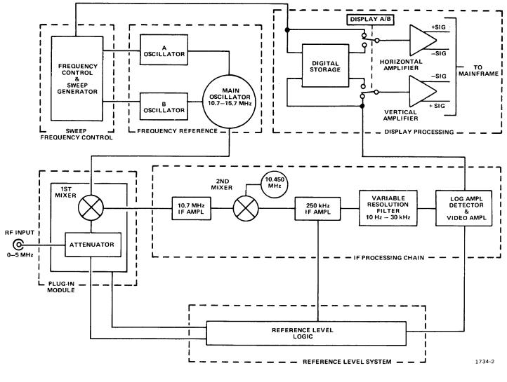
FUNCTIONAL BLOCK DESCRIPTION
Functional Block Description
The 7L5 is a swept front end spectrum analyzer with selectable front-end plug-in modules that permit the user to obtain calibrated display for a number of different Impedances (i.e., 50 ohm, 600 ohm, etc.). The plug-in module contains; selectable attenuation, the first mixer, and an Input buffer selector that trades attenuation for IF gain. Signal attenuation in the plug-in and gain of the IF processing chain are controlled by a reference level logic circuit in the 7L5 which provides calibrated settings in 1 dB or 10 dB steps over a range of approximately 146 dB (depending on the plug-in module). A simplified block diagram is shown in Fig. 3-1.
The input signal to the 7L5 is mixed with the frequency of the main oscillator and the IF of 10.7 MHz is fed to and amplified by the 10.7 MHz IF amplifier. Since the 7L5 input frequency range is O to 5 MHz, the main oscillator is tuned and swept from 10.7 to 15.7 MHz. The frequency of the main oscillator is controlled by two secondary (A and B) oscillators that use a synthesizer technique to tune and phase lock their frequencies. The sweep frequency control circuit drives the oscillators
according to the settings of front panel DOT FREQUENCY and FREQUENCY SPAN/DIV controls.
The 10 7 MHz IF is processed through bandpass filters and amplifiers and then mixed with the output from a 10.450 oscillator, to down-convert the 10.7 MHz to an IF of 250 kHz Gain of the 250 kHz amplifier is controlled by the reference level logic circuit which establishes the amount of attenuation in the plug-in module and gain for the 250 kHz IF and Log amplifiers. The reference level is selectable in 1 dB and 10 dB steps.
The 250 kHz IF signal is processed through the variable resolution filter circuits for bandwidth selections of 10 Hz to 30 kHz. The signal is again amplified, detected, and the video is sent through amplifier circuits that provide the 10 dB/dlv, 2 dB/dlv, and linear gain characteristics.
The video signal is then fed to the display processing circuits where the signal is either stored and displayed, or, if the storage mode is not selected, the signal is passed directly through the vertical output amplifier to the mainframe circuit. If either or both the DISPLAY A or DISPLAY B latches are enabled, the signal is converted to digital data, stored in A or B memory, then converted back to analog data and processed through the output amplifiers to the mainframe The vertical information is digitized and stored at 512 horizontal address locations across the screen. Therefore, the horizontal sweep information is converted to digital data for storage, then converted back to an analog signal for display The horizontal sweep ramp is processed the same as the vertical signal. The vertical (video) information can be averaged or peak detected.
3-1
TM 11-6625-2759-14 & P
Fig. 3-1. Functional block diagram.
3-2
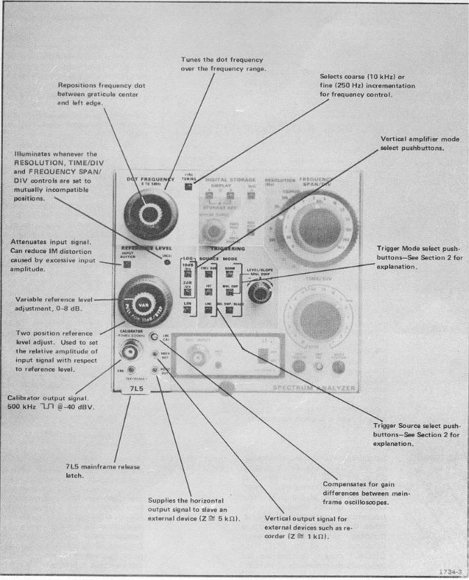
FRONT PANEL CONTROLS AND
CONNECTORS
Pushing any front panel pushbutton switch activates a bistable electronic circuit to change its output state. When in the active state, the plastic pushbutton is illuminated. Pressing the pushbutton a second time changes the output of the circuit to the inactive state and extinguishes the illuminated button.
Front panel controls also include two special photo-optic switch assemblies, the FREQUENCY SPAN/’DIV-RESOLUTION switch and the TIME/DIV switch. Designed especially for the 7L5, each assembly is a mechanical/photo-electric, digital switch, that provides a TTL compatible five-bit binary output. The reliability of these switches has been demonstrated and with normal use they should last the life of the instrument. Dismantling or field repair of these switches is discouraged since their proper operation requires precision alignment of their internal components. If either switch assembly is damaged or suspected of malfunction, it should be replaced as an assembly.
The following describes the function of the front panel selectors for the 7L5. A layout of the front panel is shown in Fig. 3-2.
DOT FREQUENCY |
Changes |
the |
dot |
(marker) |
|
|
frequency in coarse (10 kHz) or |
||||
|
fine (250 Hz) steps over the input |
||||
|
frequency range of 0 Hz to 5 MHz. |
||||
|
The frequency of the dot marker is |
||||
|
displayed on the crt readout in the |
||||
|
upper right set of characters. Dot |
||||
|
frequency will not extend beyond |
||||
|
the 7L5 frequency range, even if |
||||
|
the control is rotated. When power |
||||
|
is applied, dot frequency starts at |
||||
|
0.000. |
|
|
|
|
FINE TUNING |
Selects |
coarse |
or |
fine |
|
|
incrementation |
for |
the |
DOT |
|
|
FREQUENCY control. When the |
||||
|
FINE TUNING switch is activated |
||||
|
(illuminated), each rotational click |
||||
|
of the DOT FREQUENCY |
control |
|||
|
changes the dot frequency in |
||||
|
increments of 250 Hz. When the |
||||
|
FINE TUNING switch is inactive |
||||
|
(extinguished), |
each |
rotational |
||
|
click of the DOT FREQUENCY |
||||
|
control changes the dot frequency |
||||
|
in increments |
of |
10 |
kHz. |
|
3-3
|
|
|
TM 11-6625-2759-14 & P |
|||
DOT MKR |
Used |
to |
horizontally position |
the |
||
|
frequency |
dot. |
The |
displayed |
||
|
frequency |
readout |
characters |
|||
|
enumerate the actual frequency of the |
|||||
|
dot. When the DOT MKR control is in |
|||||
|
its detent position (fully ccw), the |
|||||
|
frequency dot and the selected |
|||||
|
frequency are on the vertical center |
|||||
|
line of the graticule. The 7L5 can be |
|||||
|
operated in a start sweep mode when |
|||||
|
the frequency dot is positioned to the |
|||||
|
left vertical graticule line. The DOT |
|||||
|
MKR control is disabled when the |
|||||
|
FREQUENCY SPAN/DIV switch is at |
|||||
|
MAX. |
|
|
|
|
|
REFERENCE |
Sets the full screen signal amplitude |
|||||
LEVEL |
level |
(dBm, dBV) |
required at |
the |
||
|
INPUT to the plug-in module. This |
|||||
|
level is relevant to the input impedance |
|||||
|
of the plug-in module. Reference level |
|||||
|
is associated to the top graticule line of |
|||||
|
the display area and signal level is |
|||||
|
relative to this |
reference. |
The |
|||
|
reference level range depends on the |
|||||
|
plug-in module, however, in the 2 |
|||||
|
dB/Div mode it covers 149 dB, in the |
|||||
|
10 dB/Div mode the range is 90 dB |
|||||
|
and in the Lin mode 20 nV/div to 200 |
|||||
|
mV/div. The control has two speeds or |
|||||
|
stepping increments; pulled out, each |
|||||
|
increment is 10 dB, pushed in each |
|||||
|
increment is 1 dB or in some cases |
|||||
|
(dependent on the plug-in module) 2 |
|||||
|
dB. |
|
|
|
|
|
VAR |
The VAR (variable) control provides 8 |
|||||
|
dB |
or |
more |
gain |
adjustment |
|
|
between |
each calibrated |
reference |
|||
|
level step. |
A<symbol is displayed on |
||||
the crt, preceding the reference level readout, whenever the reference level is not calibrated (VAR is not in its detent position).
INPUT BUFFER The active (illuminated) state of this pushbutton switch inserts 8 dB of signal attenuation at the input of the first mixer and adds 8 dB of vertical gain (after the variable resolution filters). When used, it reduces intermodulation distortion caused by excessive input signal amplitude. Because of its increased gain, the noise figure is increased 8 dB when this switch is activated.
TM 11-6625-2759-14 & P
Fig. 3-2.A. 7L5 front panel controls and connectors.
3-4

TM 11-6625-2759-14&P
Fig. 3-2B. 7LS-L1 plug-in front panel control and connectors.
@ 3-5
LOG 10 dB/DIV The illuminated condition of this pushbutton selects a logarithmic display of 10 dB/div with a dynamic range of 80 dB.
LOG 2 dB/DIV |
The |
illuminated |
condition |
of |
this |
|||
|
pushbutton |
selects |
a |
logarithmic |
||||
|
display of 2 dB/div with a dynamic |
|||||||
|
range of 16 dB |
|
|
|
|
|
||
LIN |
The |
illuminated |
condition |
of |
this |
|||
|
pushbutton selects a linear display. |
|||||||
|
Signal amplitude is a linear function of |
|||||||
|
input level. |
|
|
|
|
|
|
|
FREQUENCY |
Selects frequency |
spans |
|
from |
||||
SPAN/DIV |
50 Hz/div to 500 kHz/div (MAX |
|
||||||
|
position). A 0 Hz position provides |
|||||||
|
time domain display with a bandpass |
|||||||
|
dependent on the setting of the |
|||||||
|
RESOLUTION selector. In the 0 Hz |
|||||||
|
position the frequency dot is not |
|||||||
|
displayed and when in the MAX |
|||||||
|
position the frequency dot position is |
|||||||
|
controlled by the DOT FREQUENCY |
|||||||
|
control. |
|
|
|
|
|
|
|
RESOLUTION |
Selects resolution |
bandwidths of 10 |
||||||
|
Hz to 30 kHz in a 1-3 sequence. A |
|||||||
|
COUPLED |
position |
|
electronically |
||||
|
selects the best compatible resolution |
|||||||
|
bandwidth |
setting |
|
for |
|
the |
||
|
FREQUENCY SPAN/DIV selection. |
|||||||
TIME/DIV |
Selects the analyzer’s sweep |
rate. |
||||||
|
Sweep rates |
are 10 s/div |
to |
0.1 |
||||
|
ms/div in a 5-2-1 sequence. An AUTO |
|||||||
|
position electronically programs sweep |
|||||||
|
rate so the display remains calibrated |
|||||||
|
for the selected frequency span and |
|||||||
|
resolution bandwidth settings. |
|
|
|||||
UNCAL |
When |
the |
display |
is |
uncalibrated |
|||
|
because |
the |
|
FREQUENCY |
||||
|
SPAN/DIV, |
RESOLUTION, |
and |
|||||
|
TIME/DIV |
switch |
settings |
are |
||||
incompatible, this indicator lights and a > symbol is displayed on the crt as a prefix to the reference level readout characters.
TM 11-6625-2759-14&P
TRIGGERING Two trigger sources (Line and Internal) plus a Free Run mode can be selected. In the Free Run mode (FREE RUN button activated) the sweep free runs and will not sync with any trigger signal. When the LINE pushbutton is activated (illuminated) the sweep is triggered by the line voltage to the mainframe. The INT pushbutton selects ac coupled signal components from the mainframe Trigger Source (left or right vertical).
|
Three trigger modes are provided: |
||||
|
NORM |
(normal), |
SGL |
SWP/READY |
|
|
(single |
sweep/ready) |
and |
MNL |
|
|
SWEEP (manually controlled sweep). |
||||
|
When the NORM button is activated, |
||||
|
the sweep is triggered from the source |
||||
|
selected; or, if the trigger is not |
||||
|
present, the sweep automatically runs |
||||
|
in about 10-second intervals to provide |
||||
|
a baseline display. When the SGL |
||||
|
SWP/READY button is activated, the, |
||||
|
sweep runs with the next trigger or in |
||||
|
about 10 seconds if trigger is not |
||||
|
present. In time domain operation |
||||
|
(FREQ SPAN/DIV at 0 Hz) pushing |
||||
|
the button activates the sweep ready |
||||
|
state. The button lights to indicate the |
||||
|
trigger circuit is armed and ready. The |
||||
|
sweep will run with the arrival of a |
||||
|
trigger. |
The |
button |
remains |
|
|
illuminated until the sweep has |
||||
|
completed its run. This provides a |
||||
|
ready indication of the sweep state |
||||
|
when photographing a display. |
||||
LEVEL/SLOPE- A dual function control. As a level |
|||||
MNL SWP |
slope/control, it adjusts the level of the |
||||
|
trigger threshold on either a positive or |
||||
|
negative slope. As a manual sweep |
||||
|
control, it positions the crt beam |
||||
|
anywhere along the X- axis. |
||||
|
Maximum ccw corresponds to a beam |
||||
|
location at the left graticule edge. |
||||
DIGITAL |
SAVE A: Activating the SAVE A |
||||
STORAGE |
pushbutton dedicates one half of the |
||||
|
digital storage memory to preserve the |
||||
|
binary equivalent of the existing |
||||
|
waveform amplitude at 256 X-axis |
||||
|
locations. The A memory is inhibited |
||||
|
from further update until SAVE A is |
||||
|
deactivated (extinguished). |
|
|||
@ 3-6
DISPLAY A/B: When DISPLAY A or DISPLAY B is selected, the corresponding pushbutton switch is illuminated and the contents of memory A or memory B is displayed. With SAVE A off, all memory locations are displayed contiguously. With SAVE A on, DISPLAY A and DISPLAY B are selected. The contents of both memories are interlaced and displayed.
PEAK AVERAGE/BASELINE CLIPPER: A dual function control. When digital storage is off, this control operates as a conventional baseline clipper, i.e., as the control is rotated ccw, more of the vertical display is progressively blanked or clipped over the last 1/3 turn of the control. When digital storage is on, the PEAK AVERAGE control sets the level at which the vertical display is either peak detected or digitally averaged. Video signals above the level set by the PEAK AVERAGE control (and denoted by a horizontal cursor) are peak detected and stored. Video signals below the level set by the PEAK AVERAGE control are digitally averaged and stored.
|
MAX |
HOLD: |
Enables |
the |
digital |
||||
|
storage memory to store the |
||||||||
|
maximum signal levels within the |
||||||||
|
period |
the |
circuit |
is |
active |
(button |
|||
|
illuminated). This maximum signal |
||||||||
|
can then be saved and compared with |
||||||||
|
future |
signals |
for |
drift |
or |
amplitude |
|||
|
variations. |
|
|
|
|
|
|
|
|
SWP CAL |
Adjusted during the operational check |
||||||||
|
to calibrate |
the |
sweep. |
This |
|||||
|
adjustment |
compensates |
|
for |
|||||
|
differences |
in |
deflection |
sensitivity |
|||||
|
between |
mainframe |
oscilloscopes. |
||||||
|
The SWP CAL control should be |
||||||||
|
adjusted or checked for proper setting |
||||||||
|
each time the 7L5 is installed in an |
||||||||
|
oscilloscope. |
|
|
|
|
|
|
||
LOG CAL |
Adjusted |
during |
the |
operational |
|||||
|
check to calibrate the 2 dB/div and the |
||||||||
|
10 dB/div displays. This adjustment is |
||||||||
|
used to compensate for differences in |
||||||||
|
vertical |
gain |
between |
|
mainframe |
||||
|
oscilloscopes. The LOG CAL control |
||||||||
|
should |
be |
adjusted |
or |
checked for |
||||
TM 11-6625-2759-14&P
proper setting each time the 7L5 is installed in an oscilloscope.
AMPL CAL (L1 The AMPL CAL control is adjusted |
|
||
Plug-In Module) |
during |
the initial calibration |
to |
|
calibrate the full screen reference |
||
|
level. |
This control is used to |
|
|
compensate for gain differences in the |
||
|
RF and IF portions of the instrument. |
||
|
The AMPL CAL control should be |
||
|
adjusted or checked for proper setting |
||
|
each time a plug-in module is installed |
||
|
in the 7L5. |
|
|
HORIZ POS |
Positions the display or baseline on |
||
|
the crt X-axis. |
|
|
VERT POS |
Positions the display or baseline on |
||
|
the crt Y-axis. |
|
|
dBm/dBV |
Located on the plug-in module front |
||
|
panel, the dBm/dBV control selects |
||
|
the reference level scale factor; |
||
|
decibels with respect to one milliwatt |
||
|
or decibels with respect to one volt. |
|
|
Calibrating the 7L5 to the Oscilloscope Mainframe
1.Install or verify the presence of a plug-in module (see Optional Accessories, Section 1)
2.Select oscilloscope Vertical Mode, Horizontal Mode and Trigger Source (Right or Left) corresponding with plug-in compartments occupied by the spectrum analyzer. Turn on the mainframe power and allow a 10 minute warm-up period.
3.Set the front panel controls as follows:
DOT MKR |
max ccw (detent position) |
FREQUENCY |
|
SPAN/DIV |
MAX (500 kHz) |
RESOLUTION |
COUPLED |
VAR |
max ccw (detent position) |
BASELINE |
|
CLIPPER |
max cw |
LOG 10 dB/DIV |
on |
REFERENCE LEVEL |
-40 dBV |
INPUT BUFFER |
off |
FREE RUN |
on |
NORM |
on |
SAVE A |
off |
MAX HOLD |
off |
dBm/dBV |
dBV (plug-in module |
|
switch) |
TIME/DIV |
AUTO |
@ 3-7
4.Connect the CALIBRATOR signal to the INPUT connector on the plug-in module with a short length of coaxial cable. Adjust the SWP CAL and the HORIZ POSITION controls to align the second and tenth vertical signals with the second and tenth vertical graticule lines counting from the left edge.
5.Set the FREQUENCY SPAN/DIV to 2 kHz, Display Mode 2 dB/div, and DISPLAY A and B on. Adjust the VERT POSITION control to place the display baseline on the bottom horizontal graticule line.
6.Set RESOLUTION control to 3 kHz and DOT FREQUENCY to 500.00 kHz.
7.Select the LOG 10 dB/DIV pushbutton and adjust the LOG CAL control for a full screen (8 division) display.
8.Select the LOG 2 dB/DIV pushbutton and adjust the AMPL CAL (on plug-in module) for a full screen display.
9.Repeat steps 7 and 8 until the displayed waveforms are 8 vertical divisions in both log amplifier settings. (Refer to Fig. 3-3, Log Amplifier Calibration Composite Waveform.) If desired, check linearity of the 10 dB/div display by increasing the REFERENCE LEVEL in 10 dB steps. Adjust LOG CAL slightly to correct any nonlinearity.
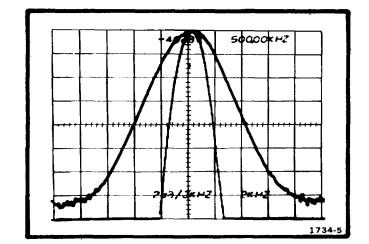
Fig. 3-3. Log amplifier calibration composite waveform.
TM 11-6625-2759-14&P
OPERATIONAL CHECKOUT
Introduction
This is an operational checkout procedure intended to satisfy most customer’s receiving inspection requirements and to provide instrument familiarization for the new user We recommend using this checkout as part of the users routine maintenance program and a preliminary check before performing the Performance Check portion of the Service Instruction manual.
The front panel CALIBRATOR output is an accurate signal source and is used in the following procedures to verify operational status of the instrument. Calibrator frequency accuracy may be verified by applying it to an accurate digital counter.
Some procedures require a step attenuator and two short lengths of coaxial cable. To verify the absolute reference level specifications, the attenuator accuracy must be calibrated or verified at some specific frequency, to within 0.03 dB/dB with a cumulative error not to exceed 0.1 dB for any change up to 10 dB. Incremental accuracy can be verified and a good indication of the absolute reference level accuracy can be obtained by using two Tektronix Step Attenuators, such as the 2701 (see Optional Accessories, Section 1). These attenuators provide a good indication of operation even though their accuracy specifications are not within the limits described.
1.Preliminary Preparation
Preset the front panel controls and selectors as described under Calibrating the 7L5 to the Oscilloscope Mainframe and perform the calibration procedure as previously described.
2.Operational Check of Readout Characters
With the 7L5 installed and operating in a 7000Series mainframe, perform the following steps to check the readout operation.
Dot Frequency Readout
a.Verify that the dot frequency readout is 0.00 kHz after initial turn-on. (Readout characters for the dot frequency are located near the top edge of the crt and can be identified by the suffix characters kHz).
b.With the FINE TUNING pushbutton not illuminated (inactive), verify that the DOT FREQUENCY control changes the value of the readout characters in 10 kHz increments.
@ 3-8

c.Rotating DOT FREQUENCY control cw should increase the readout and ccw rotation should decrease the readout.
d.Activate the FINE TUNING pushbutton and verify that the DOT FREQUENCY control changes the value of the readout characters in 250 Hz increments.
e.Verify that continuous cw rotation of the DOT FREQUENCY control causes no change of the readout characters after an indicated 4999.75 kHz.
NOTE
Following a change of the DOT FREQUENCY control, the first click in the opposite direction will have no effect.
Reference Level Readout (L1 Plug-In Module)
f.Select the LOG 2 dB/DIV mode and set the dBm/dBV switch (on the plug-in module) to dBm. Verify that the indicated value of the reference level changes by 13 dB (e.g., -40 dBV = -27 dBm). Reference level readout characters are located near the top edge of the crt and can be identified by the suffix characters dBm or dBV.
g.With the UNCAL light off, rotate the VAR (variable) control and verify that a < symbol (not calibrated) prefixes the reference level readout. Rotate the VAR control to its maximum ccw (detent) position and verify that the < symbol is no longer displayed.
h.Pull the REFERENCE LEVEL control out to its coarse position and verify that the value of the reference level readout changes in 10 dB steps. Push the REFERENCE LEVEL control in to its fine position and verify that the value of the reference level readout changes in 1 dB steps.
i.Verify, that rotation of the REFERENCE LEVEL control beyond the reference level limits of; -128 dBm (-141 dBV), In the 1 dB/step position, or; -70 dBm (- 83 dBV) in the 10 dB/step position-for the one extreme-
and +21 dBm (8 dBV) for the other extreme remains constant. (These extremes are applicable only for 50 Ò
plug-in modules.)
J. With the REFERENCE LEVEL control at max ccw position, select the LIN mode and verify that the readout changes to 200 mV.
k. Rotate the REFERENCE LEVEL cw and verify that the readout changes from mV to ÎV to nV in a 2-1-5 sequence. Verify that continuous cw rotation of the REFERENCE LEVEL control causes no change of the corresponding readout characters beyond 20 nV.
TM 11-6625-2759-14&P
Time/Div Readout
I.Set the FREQUECNY SPAN/DIV switch to
0.Rotate the TIME/DIV control to each of its positions and verify that its front panel designations correspond to the crt readout characters. (Readout characters for the sweep time per division are located near the bottom right edge of the crt and can be identified by the suffix character S when the FREQUENCY SPAN/DIV is set to 0.)
Frequency Span/Div Readout
m. Set TIME/DIV control to AUTO and the RESOLUTION control to COUPLED. Rotate the FREQUENCY SPAN/DIV control to each of Its positions and verify that the readout characters correspond with the front panel designations and change In accordance with the readout listed in Table 3-1. (Readout characters for frequency span per division setting occupy the same crt position as the time per division readout characters. They are located near the bottom edge of the crt and except for the 0 span setting, can be identified by the suffix characters Hz.)
TABLE 3-1
FREQUENCY SPAN/DIV |
FREQUENCY |
|
|
SPAN/DIV |
|
control settings |
readout |
|
0 |
10 ms |
|
50 (Hz) |
50 Hz |
|
1 kHz |
100 Hz |
|
.2 kHz |
200 Hz |
|
.5 kHz |
500 Hz |
|
1 kHz |
1 kHz |
|
2 kHz |
2 kHz |
|
5 kHz |
5 kHz |
|
10 kHz |
10 kHz |
|
20 kHz |
20 kHz |
|
50 kHz |
50 kHz |
|
.1 MHz |
100 kHz |
|
.2 MHz |
200 kHz |
|
MAX |
500 kHz |
|
Resolution Readout |
|
n. Rotate the RESOLUTION control to each of its: positions and verify that the readout characters correspond with the front panel designations. (Readout characters for the resolution function are located near the bottom edge of the crt and can be identified by the suffix characters Hz.)
@ 3-9
o. With the RESOLUTION control in the COUPLED position, rotate the FREQUENCY SPAN/DIV to each of its positions and verify that the RESOLUTION readout characters change in accord with Table 3-2.
TABLE 3-2
FREQUENCY
SPAN/DIV control settings
MAX (500 kHz) 200 kHz 100 kHz 50 kHz
20 kHz
10 kHz
5 kHz
2 kHz
1kHz
.5 kHz
2kHz
.1 kHz
50(Hz)
0
RESOLUTION
readout
30 kHz
30 kHz
30 kHz
10 kHz
3 kHz
3 kHz
1 kHz
300 Hz
300 Hz
100 Hz
30 Hz
30 Hz
10 Hz
30 kHz
Vertical Amplifier Mode Readout
p.Select the 10 dB/DIV pushbutton switch and verify that the readout characters for the vertical amplifier mode indicate 10 dB/ Readout characters for the vertical amplifier mode are located near the lower edge of the crt and for the log positions, can be identified by the suffix symbol /.
q.Select the 2 dB/DIV mode and verify that the readout characters indicate 2 dB/.
r.Push the LIN pushbutton and verify an absense of readout characters for vertical amplifier mode.
Uncalibrated Readout
s. Set the RESOLUTION control to COUPLED and the FREQUENCY SPAN/DIV control to MAX. Rotate the TIME/DIV cw until the UNCAL light is illuminated. Verify that a > symbol prefixes the referenced level readout characters. Rotate the TIME/DIV ccw until the UNCAL light is extinguished Verify that the > symbol is no longer displayed
3.Dynamic Range
TM 11-6625-2759-14&P
NOTE
The full dynamic range of the Log 10 dB/div and the Log 2 dB/div is not measured in the following paragraphs. If the log amplifiers include a negative error, full range verification would require signal level measurement below the display baseline. Since this is not possible, the following steps verify 78 of the 80 dB range and 15 dB of the 16 dB range for the two log amplifier selections.
LOG 10 dB/DIV (Dynamic window is 80 dB, accuracy is ±0.05 dB/dB to 2 dB maximum)
a.Set the 7L5 controls as follows:
DOT FREQUENCY |
500.00 kHz |
RESOLUTION |
COUPLED |
FREQUENCY SPAN/DIV |
0.1 kHz |
TIME/DIV |
AUTO |
REFERENCE LEVEL |
-40 dBV |
dBm/dBV (L1 Plug-in) |
dBV |
b. Apply the CALIBRATOR signal through external attenuator(s), such as Tektronix, 2701 (for 50 Ò)-see Optional Accessories in Section 1-to the INPUT connector. Select the LOG 10 dB/DIV pushbutton.
c. Increase external attenuation in 10 dB steps to 70 dB and verify that each step decreases the displayed f signal level 10 dB ±0.5 dB.
d. Increase external attenuation by 8 dB (for a total of 78 dB) and verify that the total overall decrease in signal amplitude is 78 dB ±2 0 dB.
LOG 2 dB/DIV (Dynamic window is 16 dB, accuracy is ±0.01 dB/dB to ±1 dB maximum)
e.Set the external attenuators to 0 dB. Set the FREQUENCY SPAN/DIV to 50 Hz, RESOLUTION to 30 Hz and select the 2 dB/DIV pushbutton.
f.Add 15 dB attenuation, with the external 1 dB step attenuator, in 2 dB and 1 dB increments. Verify that the signal level change, is within 0.1 dB/dB of added attenuation to a maximum of 1.0 dB deviation over the 15 dB range.
LIN Linearity
g. Select the LIN pushbutton and adjust the REFERENCE LEVEL control for a crt readout of 500 pV/ (per division).
@ 3-10

h.Add 10 dB of external attenuation. Adjust the VAR control for a signal display amplitude of 8 divisions.
i.Add 6 dB of external attenuation. Verify that the signal amplitude decreases to 4.0 ±0.2 division (±5%) or half amplitude.
j.Add an additional 6 dB of external attenuation and verify that the display amplitude
decreases to 2.0 ±0.1 division.
VARiable Control Range
k. Insert 10 dB of external attenuation. Select the 2 dB/DIV pushbutton and rotate the VAR control fully cw. Adjust the REFERENCE LEVEL to set the displayed signal amplitude to a vertical reference point near full screen.
I. Rotate the VAR control fully ccw (detent position). Verify that the signal amplitude decreases at least 4.0 divisions. Decrease external attenuation to return the signal amplitude to the reference point and verify that the required change was 8 dB or more.
4. Reference Level Accuracy (within 0.2 dB/dB with a cumulative error not to exceed 0.25 dB for any change up to 10 dB)
The external attenuator accuracy requirements to perform this step, have been described in the Introduction to this Operational Check procedure. Reference level increments are 1 dB and 10 dB steps. Circuitry of the 7L5 provides 1, 2, 4, 8, and 16 dB gain steps. These steps, or combinations of the steps, provide the reference level range. This procedure checks the accuracy of each gain cell and thus the overall accuracy. The accuracy of the V/Div mode will be within that specified if the Log mode reference level is within limits. A few check points may be performed as listed in Table 3-4 to spot check Lin mode operation.
This procedure uses a 50 0 plug-in module (L1):
a. Switch the dBm/dBV selector (on the plugin module) to dBm and set the 7L5 controls as follows:
REFERENCE LEVEL |
-29 dBm |
RESOLUTION |
3 kHz |
FREQEUNCY SPAN/DIV |
1 kHz |
TIME/DIV |
AUTO |
b. Set the external attenuation to 2 dB and adjust the REFERENCE LEVEL for a readout of -29 dBm. Adjust the VERT POSITION control slightly, as required to establish a graticule reference point for the signal peak.
TM 11-6625-2759-14&P
c.Change the REFERENCE LEVEL control to -30 dBm. Increase the external attenuation 1 dB (3 dB total) and verify that the signal peak is within 0.2 dB of the reference point established in step b.
d.Rotate the REFERENCE LEVEL control to - 31 dBm. Increase the external attenuation another 1 dB (4 dB total) and verify that the signal peak is within 0.25 dB of the reference point.
e.Readjust the VERT POSITION control, as required, to establish a new graticule reference point for the signal peak.
f.Pull the REFERENCE LEVEL control out to the 10 dB/step position and set it for a crt readout of -41 dBm. Increase the external attenuation 10 dB (14 dB total) and verify that the signal level is within 0.25 dB of the reference point established in step e.
g.Check the Reference Level accuracy for the remaining range by following the settings listed in Table 3-3 and noting the error.
|
TABLE 3-3 |
|
|
|
|
|
|
Reference Level |
External Attenuation |
Allowable |
|
|
|
Limits |
|
(dBm) |
(dB) |
(dB) |
|
-41 |
14 |
0.25 |
|
-51 |
24 |
0.50 |
|
-61 |
34 |
0 75 |
|
-71 |
44 |
1.00 |
|
-81 |
54 |
1.25 |
|
-91 |
64 |
1.50 |
|
-101 |
74 |
1.75 |
|
-111 |
84 |
2.00 |
|
-121 |
94 |
2.25 |
LIN Accuracy
g.Set the external attenuator to 0 dB. Select the LIN pushbutton and adjust the REFERENCE LEVEL control for a crt readout of 10 mV.
h.Set the external attenuator and the REFERENCE LEVEL control to the positions listed in Table 3-4. Check that the measured signal amplitudes are in accordance with those listed in Table 3-4.
@ 3-11

|
TABLE 3-4 |
|
||
|
|
|
|
|
|
|
Reference |
Signal |
|
Attenuator |
Voltage |
Level |
Amplitude |
|
Setting (dB) |
Input |
Volts/DIV |
in Div’s ±5% |
|
0 |
10 mV |
2 mV |
5 |
|
20 |
1 mV |
0.2 mV |
5 |
|
40 |
100 ÎV |
20 ÎV |
5 |
|
60 |
10 ÎV |
2 ÎV |
5 |
|
TM 11-6625-2759-14&P
c. Set the RESOLUTION control to 300 Hz, the FREQUENCY SPAN/DIV to 5 kHz, and the REFERENCE LEVEL to -62 dBm. Adjust the MNL control to place the trace dot halfway up one side of the displayed 300 Hz filter waveform, near center screen. Verify that maximum vertical jitter of the trace dot does not exceed 1.2 division (40 Hz)
7. Residual Response (Plug-in module dependent. Internally generated spurious signals are down 130 dB or more with the L1 Plug-In Module)
NOTE
80 |
1.0 ÎV |
200 nV |
5 |
|
5.Input Buffer (Operational check only)
a. Apply the CALIBRATOR signal to the INPUT on the plug-in module. Set the 7L5 front panel controls as follows:
DOT FREQUENCY |
500.00 kHz |
|
RESOLUTION |
|
3 kHz |
FREQUENCY SPAN/DIV |
1 kHz |
|
TIME/DIV |
AUTO |
|
INPUT BUFFER |
Off |
|
LOG 2 dB/DIV |
|
On |
b.Establish a signal amplitude of 7 divisions with the REFERENCE LEVEL control
c.Switch the INPUT BUFFER on and verify that the display amplitude does not change more than 1 dB (.05 div).
d.Change the RESOLUTION to 10 kHz and check amplitude change of the calibrator signal with the INPUT BUFFER on and off.
6.Residual (Incidental) FM (Incidental FM is <1 Hz, 50 Hz/div to 2 Hz/div and <40 kHz, 5 kHz/div to 500 kHz/div)
a.With the CALIBRATOR signal applied to the INPUT of the plug-in module, set the 7L5 front panel controls as follows:
DOT FREQUENCY |
500.00 kHz |
|
REFERENCE LEVEL |
-57 dBM |
|
RESOLUTION |
|
COUPLED |
FREQUENCY SPAN/DIV |
50 (Hz) |
|
TIME/DIV |
AUTO |
|
LOG 2 dB/DIV |
|
On |
INPUT BUFFER |
Off |
|
DIGITAL STORAGE |
Off |
|
b. Select the MNL SWP pushbutton and adjust the MNL SWP control to place the trace dot halfway up one side of the displayed 10 Hz filter waveform, near center screen. Verify that incidental FM (short term, peak to peak movement of trace dot) is less than 1.0 vertical division (1 Hz).
@ 3-12
Each 7L5 Spectrum Analyzer is carefully tested at the factory to ensure that all internally generated spurious responses are below-130 dBm. Thorough verification of this specification would take several days. A procedure to check the full frequency range (to - 110 dBm) and to spot check 100 kHz of the total frequency range, to -130 dBm is given in the following steps. The 100 kHz frequency range chosen is 300 through 400 kHz. The procedure can also be used to spot check any 200 kHz span within the 0-5 MHz capability of the instrument.
a. Terminate the input connector with a resistive load that equals the characteristic input impedance of the plugin module. Set the 7L5 front
panel controls as follows: |
|
DOT FREQUENCY |
500.00 kHz |
RESOLUTION |
300 Hz |
FREQUENCY SPAN/DIV |
100 kHz |
TIME/DIV |
AUTO |
LOG 10 dB/DIV |
On |
REFERENCE LEVEL |
-70 dBm |
INPUT BUFFER. |
Off |
BASELINE CLIPPER |
max cw |
DIGITAL STORAGE |
DISPLAY A/B |
SAVE A |
Off |
MAX HOLD |
Off |
b.Press the SGL SWP pushbutton twice to initiate a sweep. (Additional sweeps are initialiated each time the SGL SWP pushbutton is pressed.) Observe the display for spurious response (spurs). Verify that, except for the O Hz response, the amplitude of any observed spur is -110 dBm (40 dB below -70 dBm).
c.Sequentially reset the DOT FREQUENCY control to 1500 00 kHz, 2500.00 kHz, 3500.00 kHz, and 4500.00 kHz and repeat step b at each frequency setting.
d.Set the DOT FREQUENCY control to
305.00kHz, the RESOLUTION to 30 Hz, and the FREQUENCY SPAN/DIV to 1 kHz.

e.With TRIGGER SOURCE in FREE RUN, select the SGL SWP pushbutton and observe the display for spurs. Verify that the amplitude of any observed spurious response is at least 130 dB below 0 dBm. (Press SGL SWP again as required for observation.)
f.Increase the dot frequency in 10 kHz increments and repeat step e until the display is scanned from 305.00 kHz to a dot frequency of 395.00 kHz.
NOTE
To measure the amplitude of a spur, carefully reset DO T FREQUENCY to place and keep the spur within one division of center screen. Continue to reduce the frequency span per division with each sweep until maximum amplitude of the spur has been determined.
8. Sensitivity Check (Sensitivity is plug-in module dependent)
NOTE
The sensitivity for the 7L5 Spectrum Analyzer is specified with an L1 or L2 Plug-In Module using the equivalent input noise method. Sensitivity specifications and test procedures for other plug-in modules are described in the Instruction manual for the respective plug-in module.
The 7L5’s internal reference level, as indicated by the display readout, is used as the reference in the following procedure. The accuracy of the reference level readout may be verified using external test equipment and the procedure provided in the Service Instructions.
a.Set the front panel controls as follows:
DOT FREQUENCY |
1000.00 kHz |
RESOLUTION |
30 kHz |
FREQUENCY SPAN/DIV.1 kHz |
|
TIME/DIV |
10 s |
LOG 10 dB/DIV |
On |
REFERENCE LEVEL |
-70 dBm |
INPUT BUFFER |
Off |
DIGITAL STORAGE |
DISPLAY A/DISPLAY |
|
B |
TRIGGERING |
FREE RUN and NORM |
b. Terminate the INPUT in its characteristic impedance (50 0 for the L1) to prevent outside noise from entering and cluttering the display.
TM 11-6625-2759-14&P
c.Measure the average noise level by adjusting the AVERAGE LEVEL cursor above the noise peaks and noting the noise level.
d.Check the average noise level for each resolution bandwidth listed as per Table 3-5.
|
TABLE 3-5 |
|
|
|
|
RESOLUTION |
Average Noise Level |
|
30 kHz |
-105 dBm or less (35 dB below reference) |
|
10 kHz |
-110dBm or less (40 dB below reference) |
|
3 kHz |
-115 dBm or less (45 dB below reference) |
|
1 kHz |
-120 dBm or less (50 dB below reference) |
|
300 Hz |
-125 dBm or less (55dB below reference) |
|
100 Hz |
-130 dBm or less (60dB below reference) |
|
30 Hz |
-133 dBm or less (63 dB below reference) |
|
10 Hz |
-135 dBm or less (65 dB below reference) |
e. Remove the termination from the INPUT connector.
9. Resolution Bandwidth Accuracy, Amplitude
Deviation, and Shape Factor
Bandwidth accuracy; within 20% except 10 Hz position which is 100 Hz ±20 Hz, 70 dB down. Shape factor; 5:1 or better (30 kHz-3 kHz) and 10’1 or better (1 kHz-10 Hz). Amplitude deviation; less than 0 5 dB (30 kHz-100 kHz) and less than 2.0 dB (30 kHz-10 Hz).
a. Apply the CALIBRATOR signal to the INPUT on the plug-in module and set the front panel
controls as follows: |
|
DOT FREQUENCY |
500.00 kHz |
RESOLUTION |
30 kHz |
TIME/DIV |
AUTO |
DIGITAL STORAGE |
DISPLAY A/DISPLAY B |
DISPLAY MODE |
LOG 2 dB/DIV |
b.Adjust the REFERENCE LEVEL and FREQUENCY SPAN/DIV controls to establish a signal response that is 7 divisions high and about3 divisions wide at half amplitude.
c.Switch the RESOLUTION from 30 kHz to 100 Hz and reset the FREQUENCY SPAN/DIV as required so the signal amplitude deviation over the 30 kHz to 100 Hz resolution range can be observed.
d.Total deviation over the range should not exceed 0.5 dB.
@ 3-13
TM 11-6625-2759-14&P
e.Switch the RESOLUTION through the 30 kHz to 10 Ht range and check that the amplitude deviation does not exceed 2 0 dB
f.Return the RESOLUTION selector to 30 kHz, the FREQUENCY SPAN/DIV control to 10 kHz, and adjust the REFERENCE LEVEL control for a signal amplitude of 7 divisions
g.Measure the bandwidth at the 6 dB down point by using the DOT FREQUENCY control to shift the signal across a graticule reference line and noting the frequency difference from one side to the other.
h.Bandwidth must equal the RESOLUTION setting ±20 percent or 30 kHz ±6 kHz.
i.Repeat this procedure to check the -6 dB bandwidth of each RESOLUTION setting from 30 kHz through 3 kHz Verify that the bandwidth of each position is within 20 percent Note these measurements for future use when measuring the shape factor.
j.Set the RESOLUTION selector to 1 kHz, the FREQUENCY SPAN/DIV to 1 kHz or less, and adjust the REFERENCE LEVEL for a signal amplitude of 7 divisions.
k.Use the DOT MKR to adjust the signal position so the -6 dB bandwidth can be measured in graticule divisions. Convert the number of divisions to frequency by noting the setting of the FREQUENCY SPAN/DIV selector Resolution bandwidth must equal the
RESOLUTION setting ±20 percent.
I. Repeat this procedure to check the resolution bandwidth for RESOLUTION settings from 1 kHz through 30 Hz Bandwidth must equal the RESOLUTION setting ±20 percent.
m. Switch to the 10 dB/DIV display mode Set the RESOLUTION selector to 10 Hz, the FREQUENCY SPAN/DIV to 50 Hz, and adjust the REFERENCE LEVEL for a signal amplitude of 8 divisions.
@ 3-14
n. Measure the bandwidth 70 dB down by using the DOT MKR to position the display across a reference point as previously described Bandwidth must equal 100 Hz ±20 Hz (70 dB down) q
o.Return the RESOLUTION selector to 30 kHz, the FREQUENCY SPAN/DIV to 10 kHz and measure the bandwidth 60 dB down using the procedure previously described.
p.Check the shape factor (60.6 dB ratio) by measuring the 60 dB bandwidth for all RESOLUTION settings and compare this with the previous -6 dB bandwidth readings noted in steps g though I. Shape factor for RESOLUTION setting from 30 kHz to 3 kHz must equal 5:1 or better Shape factor for RESOLUTION settings from 1 kHz to 10 Hz must equal 10:1 or better.
USING THE ANALYZER
Impedance Matching
Input impedance of the 7L5 Spectrum Analyzer is determined by the plug-in module (L1, L2, L3, etc.). Impedance mismatch between a signal source and the module's input connector causes reflections or standing waves in the interconnecting transmission line and results in signal amplitude errors of the display and an overall degraded performance of the analyzer To minimize the probability of an impedance mismatch, the signal source and transmission lines, fastened to the Input connector, should have the same impedance as the plug-in module. Use cables of minimum length, and good quality. Amplitude error due to plug-in swr will be improved by turning on the 7L5's INPUT BUFFER
Signal Application
High amplitude signals (above +21 dBm or 2.5 V rms) will overload and damage the mixer circuit and should not be applied to the input connector (See the plug-in instruction manual for maximum allowable input power ) Signals of unknown amplitude should be routed through a attenuator If spurious or multitone intermodulation signals are present on the display, or, if saturation of the mixer is suspected, the 7L5 INPUT BUFFER will add 8 dB of attenuation in series with the input signal. If the displayed signals show little or no change with the buffer on, the intermodulation or spurious signals are not generated by the spectrum analyzer.
Edge Noise
When using the digital storage mode, some applications may leave display remnants at the edges of the crt. This condition is an unavoidable result of the storage memory being wider than the crt screen and not a malfunction. Edge noise is removed as follows: 1) Disconnect any signal from the INPUT connector. 2) With digital storage on the FREQUENCY SPAN/DIV set to other than MAX, rotate DOT MKR control to max cw position 3) After one sweep has occurred, to extend the baseline, rotate the DOT MKR control max ccw to the detent position. 4) Wait one sweep to clear the left edge then apply the input signal.
Frequency Measurement Technique
Frequency measurement should be made on the second or subsequent sweeps after the DOT FREQUENCY has been changed. (Oscillator stabilization time is 1 second or less.)
Following a change of the DOT FREQUENCY control, the first click in the opposite direction will have no effect. This is due to the electronic coupling within the DOT FREQUENCY control assembly.
Max Span Operation
When the 7L5 is operated with the FREQUENCY SPAN/DIV control set to MAX (500 kHz), optimum instrument performance will be ensured by setting the RESOLUTION to 30 kHz or COUPLED position. The COUPLED position will maintain a desired ratio of 20:1 or less between the frequency span per division and the resolution bandwidth.
Resolution, Resolution Bandwidth
The, term resolution represents an instrument’s ability to display adjacent signal responses discretely. A measure of resolution is the frequency separation in hertz of responses which merge with a 3 dB notch. Displayed resolution is a function of spectrum analyzer bandwidth, horizontal sweep rate and frequency span. Resolution is also affected by incidental (residual) FM.
Resolution bandwidth, as defined for the 7L5, is the width in hertz between 6 dB down image points, on the curve of the analyzer’s displayed response, to a cw input signal.
TM 11-6625-2759-14&P
Bandwidth determines both the noise level and resolution capability of the analyzer. As bandwidth decreases, both sensitivity and signal-to-noise ratio improve. Maximum sensitivity is obtained when resoltuion bandwidth is narrow (10-30 Hz).
For most applications, the analyzer should be used with the RESOLUTION control set to COUPLED and the TIME/DIV switch set to AUTO. These autoranged positions provide the best sweep rate and resolution bandwidth for each setting of the FREQUENCY SPAN/DIV switch. When the analyzer is used to make amplitude measurements, especially in digital storage mode, the COUPLED and AUTO positions of these controls ensures maximum accuracy.
Digital Storage Use
When using digital storage, the best measurement accuracy is obtained by setting the following controls as follows; (see Fig. 3-2, Front Panel Controls.)
1. |
VIDEO |
Adjust to place the cursor at a point |
|
PEAK/VIDEO |
midway between maximum signal |
|
AVERAGE: |
amplitude and baseline noise. |
2. |
DISPLAY A/ |
Press both pushbuttons to activate |
|
DISPLAY B |
storage operation |
3. |
RESOLUTION |
Set to COUPLED position. |
4. |
TIME/DIV |
Set to AUTO position or a position |
|
|
that is compatible with the setting of |
|
|
FREQUENCY SPAN/DIV control |
|
|
(UNCAL light not illuminated). |
Applications for Spectrum Analyzers
Applications for spectrum analyzers such as the 7L5 include; measuring intermodulation products, radiation interference, modulation percentage, absolute and relative signal level measurements, bandpass characteristics, etc. Numerous application notes on spectrum analyzer measurements are available from your local Tektronix Field Office or representative, including assistance for specific measurement applications you may desire.
@ 3-15
|
|
|
|
|
TM 11-6625-2759-14&P |
|
|
|
|
|
PART II |
|
|
|
|
|
|
TABLE OF CONTENTS |
Page |
|
Section |
1 |
GENERAL INFORMATION |
||||
|
||||||
|
|
Introduction and Description .......................................................................................... |
1-1 |
|||
|
|
Manual Organization ...................................................................................................... |
1-2 |
|||
|
|
Electrical Characteristics................................................................................................ |
1-2 |
|||
|
|
|
Frequency ............................................................................................................... |
1-2 |
||
|
|
|
Input ........................................................................................................................ |
1-3 |
||
|
|
|
Amplitude ................................................................................................................ |
1-3 |
||
|
|
|
Sweep ..................................................................................................................... |
1-4 |
||
|
|
|
Output Connectors.................................................................................................. |
1-4 |
||
|
|
Environmental Characteristics ....................................................................................... |
1-5 |
|||
|
|
Physical Characteristics ................................................................................................. |
1-5 |
|||
|
|
Accessories and Options ............................................................................................... |
1-5 |
|||
|
|
Installation ...................................................................................................................... |
1-5 |
|||
|
|
Repackaging for Shipment ............................................................................................. |
1-6 |
|||
Section |
2 |
CIRCUIT DESCRIPTION |
|
|||
|
|
Block Diagrams .............................................................................................................. |
2-1 |
|||
|
|
|
IF Processing Chain ............................................................................................... |
2-1 |
||
|
|
|
Sweep Control and Frequency Reference .............................................................. |
2-2 |
||
|
|
|
Frequency Control Circuits .................................................................................... |
2-3 |
||
|
|
|
Readout .................................................................................................................. |
2-5 |
||
|
|
|
Display Processing ................................................................................................. |
2-6 |
||
|
|
Detailed Circuit Description ............................................................................................ |
2-7 |
|||
|
|
|
Sweep Control ........................................................................................................ |
2-7 |
||
|
|
|
Trigger Logic and Sweep Control ........................................................................... |
2-11 |
||
|
|
|
Frequency Span and Readout ................................................................................ |
2-13 |
||
|
|
|
Tune Reference- N Loops....................................................................................... |
2-13 |
||
|
|
|
A&B Oscillator and Control ..................................................................................... |
2-14 |
||
|
|
1st LO/1st LO Lock ........................................................................................................ |
2-15 |
|||
|
|
|
Reference Level, Readout, and Timeslot ................................................................ |
2-15 |
||
|
|
|
Readout and Timeslot Decode ............................................................................... |
2-18 |
||
|
|
|
IF Processing Chain ............................................................................................... |
2-19 |
||
|
|
|
Variable Resolution................................................................................................. |
2-20 |
||
|
|
|
10 kHz & 30 kHz Filters and Post VR Amplifier ...................................................... |
2-22 |
||
|
|
|
Log/Lin Amplifier ..................................................................................................... |
2-22 |
||
|
|
|
Detector and Video Amplifier .................................................................................. |
2-22 |
||
|
|
Display Processing ........................................................................................................ |
2-23 |
|||
|
|
|
Horizontal and Vertical Display Processing ............................................................ |
2-23 |
||
|
|
|
Average Calculator ................................................................................................. |
2-24 |
||
|
|
|
Digital Storage ........................................................................................................ |
2-25 |
||
Section |
3 |
PERFORMANCE CHECK |
|
|||
|
|
Introduction .................................................................................................................... |
3-1 |
|||
|
|
Equipment Required or Recommended ......................................................................... |
3-1 |
|||
|
|
|
1. |
Sweep Triggering ............................................................................................... |
3-2 |
|
|
|
|
2. Dot Frequency Range and Accuracy ................................................................. |
3-2 |
||
|
|
|
3. |
Display Flatness ................................................................................................ |
3-3 |
|
|
|
|
4. |
Frequency Span Accuracy & Linearity ............................................................... |
3-4 |
|
|
|
|
5. Sweep Rate Accuracy........................................................................................ |
3-5 |
||
|
|
|
6. |
Intermodulation Distortion .................................................................................. |
3-6 |
|
|
|
|
7. |
Display Frequency Stability................................................................................ |
3-7 |
|
Section |
4 |
CALIBRATION PROCEDURE |
|
|||
|
|
Complete or Partial Calibration ...................................................................................... |
4-1 |
|||
|
|
History Information ......................................................................................................... |
4-1 |
|||
|
|
Interaction. ..................................................................................................................... |
4-1 |
|||
|
|
Equipment Required ...................................................................................................... |
4-2 |
|||
|
|
Short Form Procedure and Record ................................................................................ |
4-2 |
|||
|
|
Preliminary Procedure ................................................................................................... |
4-3 |
|||
|
|
1. |
Check/Adjust the Reference Oscillator Frequency ................................................... |
4 -6 |
||
|
|
2. |
Check/Adjust the Calibrator Output Level ................................................................. |
4-6 |
||
|
|
|
|
TM 11-6625-27S9-14&P |
|
|
|
|
Page |
|
|
3. |
Frequency Span/Div Calibration ........................................................................ |
4-7 |
|
|
4. Sweep Timing .................................................................................................... |
4-9 |
|
|
|
5. |
1st LO and 1st LO Phase Lock Calibration ........................................................ |
4-10 |
|
|
6. |
Function IF Calibration ....................................................................................... |
4-11 |
|
|
7. |
Calibrate the 250 kHz, 2nd Mixer, and 10.7 MHz Input Filter ............................ |
4-12 |
|
|
8. |
Variable Resolution Calibration ......................................................................... |
4-13 |
|
|
9. |
Digital Storage Calibration ................................................................................. |
4-16 |
|
|
Calibration Test Equipment Replacement Chart ..................................................... |
4-19 |
|
Section |
5 |
MAINTENANCE |
|
|
|
|
Introduction .................................................................................................................... |
5-1 |
|
|
|
Preventive Maintenance................................................................................................. |
5-1 |
|
|
|
Cleaning......................................................................................................................... |
5-1 |
|
|
|
Lubrication ..................................................................................................................... |
5-2 |
|
|
|
Visual Inspection ............................................................................................................ |
5-2 |
|
|
|
Transistor and Integrated Circuit Checks ....................................................................... |
5-2 |
|
|
|
Troubleshooting ............................................................................................................. |
5-2 |
|
|
|
Troubleshooting Aids .............................................................................................. |
5-2 |
|
|
|
Finding Faulty Semiconductors .............................................................................. |
5-3 |
|
|
|
General Troubleshooting Techniques ............................................................................ |
5-5 |
|
|
|
Corrective Maintenance ................................................................................................. |
5-5 |
|
|
|
Disassembly of the 7L5 and Replacing Assemblies ...................................................... |
5-7 |
|
|
|
Removing the Front Panel ............................................................................................. |
5-7 |
|
|
|
Removing the IF Module Assembly ............................................................................... |
5-7 |
|
|
|
Removing the Sweep Board .......................................................................................... |
5-8 |
|
|
|
Removing the RF Module .............................................................................................. |
5-9 |
|
|
Reassembling the 7L5 .......................................................................................................... |
5-9 |
||
Section |
6 |
OPTION INFORMATION |
|
|
Section |
7 |
REPLACEABLE ELECTRICAL PARTS ......................................................................... |
7-1 |
|
|
|
Part Number-NSN Index ................................................................................................ |
7-42 |
|
Section |
8 |
DIAGRAMS AND CIRCUIT BOARD ILLUSTRATIONS |
|
|
Section |
9 |
REPLACEMENT MECHANICAL PARTS AND EXPLODED DRAWINGS |
|
|
Section |
10 |
DIFFERENCE DATA SHEETS ...................................................................................... |
10-1 |
|
Appendix |
A. |
References..................................................................................................................... |
A-1 |
|
Appendix |
B. |
Operator’s, Organizational, Direct Support, and General Support |
|
|
|
|
Maintenance Repair Parts and Special Tools List ......................................................... |
B-1 |
|
Appendix |
C. |
Maintenance Allocation Chart ........................................................................................ |
C-1 |
|

TM 11-6625-2759-14&P
SECTION 1. GENERAL INFORMATION
INTRODUCTION AND DESCRIPTION
To effectively use the 7L5 Spectrum Analyzer, the operation and capabilities of the instrument must be known. This instruction manual covers general service information for the instrument. It contains the specification, test and calibration procedure, circuit description, and maintenance procedure for the 7L5.
The 7L5 is a 5 MHz spectrum analyzer with digital storage. Frequency stability is within 5 Hz/hr and center frequency (dot) can be read with six digit accuracy immediately after turn-on; therefore there is no need to fine tune the display. Complex measurements and analysis can be made with relative ease. Built-in microprocessing circuits decode control settings, process frequency and reference level information, and optimize sweep time and resolution for the selected frequency span. At turn-on, the 7L5 is preset to a reference level of +17 dBm (50 Ò input) and center frequency of 00.0 kHz. This provides input attenuation to protect the front-end circuitry and a marker to verify correct operation.
The 7L5 with 80 dB or more of spurious free dynamic range provides the ability to measure wide relative amplitudes. Nanovolt sensitivity provides very low-level signal and noise requirements.
The 7L5 display is fully calibrated in dBm, dBV, or volts/div. The reference level can be accurately set in 1 dB increments.
A front panel input buffer control increases frontend immunity to intermodulation distortion while maintaining a constant reference level.
To accommodate a wide variety of impedance sources, the 7L5 uses quick disconnect plug-in input impedance modules of 50 Ò, 75 Ò, 600 0, 1 MÒ/28 pF and customized units to meet special requirements.
When the 7L5’s digital storage capability is employed, one or two complete displays can be held in memory for subsequent viewing, comparison, or graphic reproduction. This capability converts a nonstorage, 7000-Series oscilloscope display into a stored display. The small dot size (of the conventional oscilloscope) used with the 7L5 enhances the resolution of low amplitude signals and other fine details that are often lost with a variable persistence oscilloscope. In storage mode, the vertical display may be bisected by an averaging threshold, above which video peak detection occurs (prior to storage) and below which video signal averaging occurs (prior to storage). Denoted by a cursor, the averaging threshold is continuously adjustable with a front panel control. The storage circuitry includes a maximum hold capability. This feature allows monitoring of signals that may change with time to provide a graphic record of amplitude/frequency excursion.
The following service instructions are for personnel qualified to service electronic circuits. Personnel not familiar with electrical circuit operation should not perform any service other than that contained in the Operating Instuction manual.
@ 1-1
MANUAL ORGANIZATION AND CONTENT
The abbreviations, graphic symbols, and logic symbology used in the text and diagrams of this manual are in accord with and based on ANSI Y1.1-1972, ANSI Y 32.3-1975, and ANSI Y32.14-1973 (American National Standard Institute, 345 East 47 Street; New York, N.Y. 10017).
Change information is contained on insert pages at the back of the manual. Original pages are identified by the symbol @ and revised pages are identified by a revision date in the lower inside corner of the page. If the serial number of your instrument is lower than the one on the title page, the manual contains revisions that may not apply to your instrument. History information, applicable to previous products, with the updated data, is integrated when the page or diagram is revised. The following describes the sections and information provided in this manual.
Section 1-General Information: Contains the instrument description and specification.
Section 2-Circuit Description: Provides basic and general circuit theory. This information may be useful when servicing or operating the instrument.
Section 3-Performance Check: Procedure.; to verify that the instrument is performing within its specified limits.
Section 4-Calibration Procedure: Test equipment setup and adjustment procedures required to calibrate the instrument.
Section 5-Maintenance: Describes routine and corrective maintenance procedures with detailed instructions for replacing assemblies, sub-assemblies, or individual components. An exploded drawing is part of Section 9. Troubleshooting procedures plus general information that may aid in servicing the instrument are also provided.
Section 6-Options Information: Describes options to the instrument or directs the reader to where the options are documented.
Section 7-Replaceable Electrical Parts: Provides information necessary to order replaceable parts and assemblies.
TM 11-6625-2759-14&P
Section 8-Diagrams: Functional block diagrams and detailed circuit schematics are provided. Located adjacent to the diagram (usually on the back of the preceding diagram) are pictorial layout drawings that show subassembly and component locations. Integrated circuit diagrams, waveforms and voltage data for troubleshooting or circuit analysis are also provided adjacent to or on the diagram.
Section 9-Replaceable Mechanical Parts, Exploded Drawings and Accessories: Provides information necessary to order replaceable parts. The Replaceable Parts list is cross-referenced to the Replaceable Electrical Parts list. The exploded drawing identifies assemblies and mechanical components.
Change Information: Provides updating information in the form of inserts for the manual. These inserts are later incorporated into the manual text and diagrams when the manual is reprinted.
ELECTRICAL CHARACTERISTICS
The following electrical characteristics apply when the 7L5 Spectrum Analyzer, in combination with a Plug-In Module, are normally installed in a 7000-Series oscilloscope and after a warm-up of ten minutes or more.
Frequency Characteristics
Range
Input Frequency: 10 Hz through 5.0 MHz.
Dot Frequency: 0 Hz through 4999.75 kHz.
Accuracy
20°C to 30° C: ±(5 Hz + 2 x 10⁻⁶ of dot readout).
0°C to 50 °C: +(20 Hz + 10-5 of dot readout).
Drift
5 Hz/hour or less.
Residual (Incidental) FM
50 Hz/div to 2 kHz/div: 1 Hz (p-p) or less.
5 kHz/div to 500 kHz/div: 40 Hz (p-p) or less.
@ 1-2
 Loading...