


QT-CD111/111C
SERVICE MANUAL
No. S3819QTCD111/
QT-CD111
QT-CD111C
Illustration: QT-CD111 |
• In the interests of user-safety the set should be restored to its |
|
original condition and only parts identical to those specified should |
|
be used. |
|
|
CONTENTS |
|
|
Page |
IMPORTANT SERVICE NOTES (FOR QT-CD111 ONLY) ................................................................................................ |
2 |
SPECIFICATIONS ............................................................................................................................................................. |
2 |
NAMES OF PARTS ........................................................................................................................................................... |
3 |
DISASSEMBLY .................................................................................................................................................................. |
4 |
REMOVING AND REINSTALLING THE MAIN PARTS ..................................................................................................... |
5 |
ADJUSTMENT ................................................................................................................................................................... |
6 |
BLOCK DIAGRAM ............................................................................................................................................................. |
8 |
SCHEMATIC DIAGRAM / WIRING SIDE OF P.W.BOARD ............................................................................................. |
10 |
NOTES ON SCHEMATIC DIAGRAM .............................................................................................................................. |
16 |
TYPES OF TRANSISTOR ............................................................................................................................................... |
16 |
WAVEFORMS OF CD CIRCUIT ...................................................................................................................................... |
17 |
TROUBLESHOOTING (CD SECTION) ........................................................................................................................... |
18 |
FUNCTION TABLE OF IC ................................................................................................................................................ |
21 |
PARTS GUIDE/EXPLODED VIEW |
|
PACKING OF THE SET (FOR QT-CD111 ONLY) |
|
SHARP CORPORATION |
This document has been published to be used |
for after sales service only. |
|
– 1 – |
The contents are subject to change without notice. |
|
QT-CD111/111C
FOR A COMPLETE DESCRIPTION OF THE OPERATION OF THIS UNIT, PLEASE REFER TO THE OPERATION MANUAL.
IMPORTANT SERVICE NOTES (FOR QT-CD111 ONLY)
BEFORE RETURNING THE AUDIO PRODUCT
(Fire & Shock Hazard)
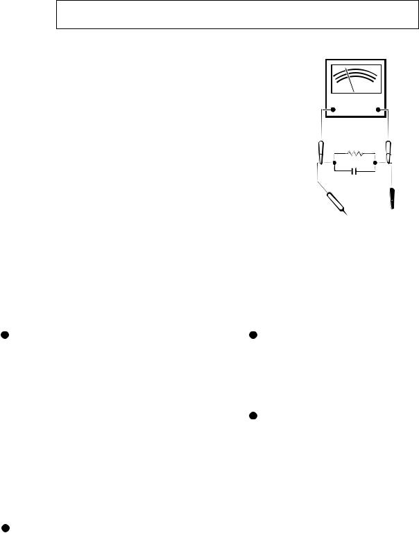
Before returning the audio product to the user, perform the following safety checks.
1.Inspect all lead dress to make certain that leads are not pinched or that hardware is not lodged between the chassis and other metal parts in the audio product.
2.Inspect all protective devices such as insulating materials, cabinet, terminal board, adjustment and compartment covers or shields, mechanical insulators etc.
3.To be sure that no shock hazard exists, check for leakage current in the following manner.
*Plug the AC line cord directly into a 120 volt AC outlet.
*Using two clip leads, connect a 1.5k ohm, 10 watt resistor paralleled by a 0.15μF capacitor in series with all exposed metal cabinet parts and a known earth ground, such as conduit or electrical ground connected to earth ground.
*Use a VTVM or VOM with 1000 ohm per volt, or higher, sensitivity to measure the AC voltage drop across the resistor (See diagram).
*Connect the resistor connection to all exposed metal parts having a return path to the chassis (antenna, metal cabinet, screw heads, knobs and control shafts, escutcheon, etc.) and measure the AC voltage drop across the resistor.
VTVM
 AC SCALE
1.5k ohms
10W
0.15 µ F
TO EXPOSED
TEST PROBE  CONNECT TO
METAL PARTS
KNOWN EARTH
GROUND
All check must be repeated with the AC line cord plug connection reversed.
Any reading of 0.3 volt RMS (this corresponds to 0.2 milliamp. AC.) or more is excessive and indicates a potential shock hazard which must be corrected before returning the audio product to the owner.
SPECIFICATIONS
General |
|
Tape recorder |
|
Power source: |
AC 120V, 60 Hz |
Frequency response: |
50 - 14,000 Hz (Normal tape) |
|
DC 12 V [ "D" size (UM/SUM-1, |
Signal/noise ratio: |
50 dB |
|
R20 or HP-2) battery x 8] |
Wow and flitter: |
0.25 % (WRMS) |
Power consumption: |
20 W |
Motor: |
DC 12 V electric governor |
Output power: |
FTC; 2.0 W min. RMS per channel |
Bias system: |
AC bias |
(111) |
into 8 ohms from 150 Hz to 20 kHz, |
Erase system: |
Magnet erase |
|
with no more than 10 % total harm- |
Compact disc player |
|
|
onic distortion. |
||
|
RMS; 2.3 W (1.65 W + 1.65 W) |
Disc: |
Compact disc |
|
(DC operation, 10 % T.H.D.) |
Signal readout: |
Non-contact, 3-beam semi- |
Output power: |
RMS; 2.3 W/CH |
|
conductor laser pickup |
(111C) |
(DC operation, 10 % T.H.D.) |
Audio channels: |
2 |
Speakers: |
4" (10 cm) full-range speaker x 2 |
Quantization: |
16-bit linear quantization |
Dimensions: |
Width; 18-15/16" (480 mm) |
Filter: |
4-tims oversampling digital filter |
|
Height; 6-1/16" (153 mm) |
D/A converter: |
1-bit D/A converter |
|
Depth; 10" (254 mm) |
Wow and flutter: |
Unmeasurable |
Weight: |
7.1 Ibs. (3.2 kg) without batteries |
|
(less than 0.001% W. peak) |
Radio |
|
|
|
|
Specifications for this model are subject to change without |
||
Frequency range: |
FM; 87.6 - 108 MHz |
||
|
AM; 530 - 1,702 kHz |
prior notice. |
|
|
|
|
|
– 2 –
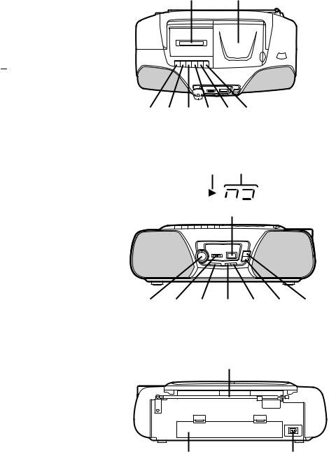
1.Cassette Compartment
2.CD Compartment
3.Tuning Control
4.(TAPE) Record Button: 
5.(TAPE) Play Button: 
6.(TAPE) Rewind Button: 
7.(TAPE) Fast Forward Button: 
8.(TAPE) Stop/Eject Button:  /
/
9.(TAPE) Pause Button: 

QT-CD111/111C
NAMES OF PARTS
1 2


 3
3
4 5 6 7 8 9
10.(CD) Play Indicator: 
11.(CD) Track Number Indicator
12.(CD) Repeat Indicator: 
13.Volume Control
14.Function Selector/Power Switch
15.Extra Bass Button: X-BASS
16.(CD) Track Down/Review Button: 


17.(CD) Track Up/Cue Button: 


18.(CD) Stop Button: 
19.(CD) Play/Repeat Button: 
10 11
12 


13 14 15 |
16 17 18 |
19 |
20. FM Telescopic Rod Aerial 20
21. Battery Compartment
22. AC Power Input Socket
21 22
– 3 –

QT-CD111/111C
DISASSEMBLY
Caution on Disassembly
Follow the below-mentioned notes when disassembling the unit and reassembling it, to keep it safe and ensure excellent performance:
1.Take cassette tape and compact disc out of the unit.
2.Be sure to remove the power supply plug from the wall outlet before starting to disassemble the unit.
3.Take off nylon bands or wire holders where they need be removed when disassembling the unit. After servicing the unit, be sure to rearrange the leads where they were before disassembling.
4.Take suffcient care on static electricity of integrated circuits and other circuits when servicing.
STEP |
REMOVAL |
|
PROCEDURE |
FIGURE |
|
|
|
|
|
|
|
1 |
Rear Cabinet |
1. |
Screw ................. |
(A1) x10 |
4-1 |
|
|
2. Socket .................. |
(A2) x1 |
4-2 |
|
|
|
|
|
|
|
2 |
Top Cabinet |
1. |
Knob ..................... |
(B1) x1 |
4-2 |
|
(with CD Mechanism/ |
2. |
Screw ................... |
(B2) x3 |
|
|
Tape Mechanism/ |
3. |
Socket .................. |
(B3) x1 |
|
|
Main PWB) |
|
|
|
|
|
|
|
|
|
|
3 |
Main PWB/ |
1. |
Screw ................... |
(C1) x6 |
4-3 |
|
Switch PWB |
2. |
Socket .................. |
(C2) x4 |
4-3,4-4 |
4 |
Tape Mechanism |
1. |
Screw ................... |
(D1) x4 |
4-4 |
|
|
|
|
|
|
5 |
CD Mechanism |
1. Screw ................... |
(E1) x3 |
4-4 |
|
|
|
|
|
|
|
6 |
Terminal PWB |
1. Screw ................... |
(F1) x4 |
4-5 |
|
|
|
2. |
Hook ..................... |
(F2) x1 |
|
|
|
|
|
|
|
Front Cabinet
(A1)x6
ø3x20mm
(A1)x3 |
Rear Cabinet |
ø3x12mm |
|
(A1)x1
ø3x12mm
Figure 4-1
Top Cabinet
(B1)x1
(B2)x3 |
Main PWB |
ø3x10mm |
(A2)x1 |
|
(B3)x1 |
Front Cabinet
|
(C2)x1 |
|
(C1)x5 |
Switch PWB |
|
ø3x10mm |
||
|
Main PWB
Top Cabinet
(C1)x1
ø3x10mm
Figure 4-3
(D1)x4  ø3x10mm
(E1)x3
ø2.5x10mm
Tape
Mechanism
(C2)x2

Top Cabinet
(C2)x1
CD Mechanism
Figure 4-4
(F2)x1
Push
Driver
(F1)x2  ø3x10mm
 Terminal PWB
(F1)x2
ø3x10mm
Figure 4-2 |
Figure 4-5 |
– 4 –
QT-CD111/111C
REMOVING AND REINSTALLING THE MAIN PARTS
CD MECHANISM SECTION
Perform steps 1, 2, 3 and 5 of the disassembly method to remove the CD mechanism.
How to remove the pickup (See Fig. 5.)
1.Remove the screws (A1) x 2 pcs., to remove the shaft (A2) x1 pc.
2.Remove the stop washer (A3) x1 pc., to remove the gear (A4) x 1 pc.
3.Remove the pickup.
|
(A1) x2 |
|
2.6 x6mm |
Pickup |
CD |
|
Mechanism |
|
|
Stop |
|
Shaft |
|
Washer |
|
Gear |
(A3) x1 |
||
(A2) x1 |
|||
(A4) x1 |
|
||
|
|
Figure 5
– 5 –
QT-CD111/111C
ADJUSTMENT
MECHANISM SECTION
• Driving Force Check
Torque Meter |
Specified Value |
|
|
PLAY: TW-2412 |
Over 120 g |
|
|
• Torque Check
Torque Meter |
Specified Value |
|
|
Play: TW-2111 |
25 to 65 g.cm |
|
|
Fast Forward: TW-2231 |
60 to 130 g.cm |
|
|
Rewind: TW-2231 |
60 to 130 g.cm |
|
|
• Head Azimuth
Torque Meter |
Specified Value |
|
|
MTT-114 |
Output: Speaker Terminal |
|
(CNP201 Load resistance: 8 ohms) |
|
|
• Tape Speed
Test |
Adjusting |
Specified |
Instrument |
Tape |
Point |
Value |
Connection |
MTT-111 |
In motor |
3,000 ± 90 Hz |
Output: Speaker |
|
|
|
Teaminal |
|
|
|
(CNP201 Load |
|
|
|
resistance: 8 ohms) |
|
|
|
|
TAPE SECTION
Position of each switch or control
Volume control |
Max |
Function switch |
Tape/Power Off |
X-BASS |
On |
|
|
• Bias Oscillation
Adjustment Point |
Specified Value |
Instrument |
|
|
Connection |
|
|
|
L301 |
82 kHz ± 6 kHz |
Pin 2 of CNP201 |
|
– 6 kHz |
|
|
|
|
• Playback Amplifier Sensitivity Check
Test Tape |
Specified Value |
Instrument Connection |
|
|
|
MTT-118 |
1.8 V ± 3 dB |
Speaker Terminal |
|
|
(Load resistance: 8 ohms) |
|
|
|
MAIN PWB
AM |
|
|
|
|
|
|
TRACKING |
|
|
|
FM ROD ATENNA |
|
|
fL |
|
|
|
|
||
|
|
|
|
|
|
|
|
|
|
|
VR1 |
|
|
|
|
|
VCO |
|
|
|
|
|
|
|
|
13 |
|
L3 |
ANTENNA |
FM |
T2 |
1917 IC2 |
T3 |
|
|
|
1 |
||||
|
|
DETECTION |
21 |
|
||
|
BAR |
|
L4 |
L2 |
|
AM IF |
|
|
|
|
|||
|
|
|
|
|
|
|
AM |
|
|
TC4 |
|
IC1 |
T1 |
|
|
|
|
|
||
|
|
|
|
TC2 |
|
|
|
|
|
TC3 |
TC1 |
|
FM IF |
|
|
|
|
|
||
|
|
|
|
|
|
|
|
|
AM |
|
L1 |
1 |
|
|
|
TRACKING |
|
|
|
|
|
|
fH |
|
|
|
|
fH |
fL |
|
fH |
fL |
fH |
fL |
AM BAND |
|
FM |
|
FM BAND |
||
COVERAGE |
|
TRACKING |
COVERAGE |
|||
TUNER SECTION
fL: Low-range frequency fH: High-range frequency
• FM IF/RF
Test Stage |
Specified |
Instrument |
|
|
Value/Adjusting |
Connection |
|
|
Point |
|
|
IF |
T1 |
Input: Pin 1 of IC1 |
|
|
|
Output: Pin 17 of IC2 |
|
Detection |
T2 |
||
|
|||
|
|
|
|
Band Coverage |
fL: L2 |
Iuput: Antenna |
|
|
fH: TC2 |
Output: Speaker |
|
|
|
Terminal (CNP201 |
|
Tracking |
88.0 MHz: L1 |
||
Load resistance: 8 |
|||
|
108.0 MHz: TC1 |
||
|
ohms) |
||
|
|
||
|
|
|
• AM IF/RF
Test Stage |
Specified |
Instrument |
|
Value/Adjusting |
Connection |
|
Point |
|
IF |
T3 |
Input: Antenna |
|
|
Output: Pin 19 of IC2 |
|
|
|
Band Coverage |
fL: L4 |
Input: Antenna |
|
fH: TC4 |
Output: Speaker |
Tracking |
600 kHz: L3 |
Terminal (CNP201 |
|
1,400 kHz: TC3 |
Load resistance: 8 |
|
|
ohms) |
|
|
|
• VCO Frequency
Adjusting Point |
Specified |
Instrument |
|
Value |
Connection |
|
|
|
VR1 |
76 kHz ± 200 Hz |
Pin 13, pin 21 and |
|
|
ground of IC2 |
|
|
|
Note:
After preparing the test circuit shown in Fig. 6-1, connect the Pin 13, Pin 21 and ground of the IC2 with the test circuit, and measure the value. At this time, apply a standard unmodulated signal input and adjust the VCO.
Pin 13 of IC2 Pin 21 of IC2 |
|
||
G |
D |
FET : 2SK19 or 2SK54 |
|
|
|
||
|
|
|
|
|
S |
|
TO FREQUENCY |
|
|
|
COUNTER |
10 kohm
Figure 6-1 VCO FREQUENCY TEST CIRCUIT
Figure 6-2 ADJUSTMENT POINTS
– 6 –
QT-CD111/111C
CD SECTION
Since this CD system incorporates the following automatic adjustment function, when the pickup is replaced, it is necessary to reajust it.
Since this CD unit does not need adjustment, the combination of PWB and laser pickup unit is not restricted.
TEST MODE
Start |
While holding down the "STOP" button, move the FUNCTION/POWER switch to "CD". |
|
Then, release the "STOP" button and, within 0.5 second, connect the TEST POINT to GND (within 0.5 second). |
||
|
||
|
(See Fig. 7) |
|
|
|
|
Note |
1. When the CD LID switch is in the OFF position, the unit will be able to enter the test mode. |
|
However, playback cannot be performed in this mode. |
||
|
2.You can only move the pickup.
3.The LCD display should be the same as it is for normal CD operations.
Operation |
1 |
The use of the "UP/CUE" button will move the pickup to the outermost position. |
|
The use of the "DOWN/REVIEW" button will move the pickup to the innermost position. |
|||
|
|
||
|
|
|
|
|
2 |
When the "PLAY" button is pressed, the laser will be lit, and when the "STOP" button is pressed, it will be |
|
|
turned off. Playback will also start and stop when these buttons are pressed. |
||
|
|
a.If the "PLAY" button is pressed while in the stop mode, the laser will simply be turned on at first.
b.If the laser is lit and the "PLAY" button is pressed again, playback will start from the current pickup position.
c.If the "STOP" button is pressed, playback will stop. When pressed again, the laser will be turned off.
3Turning the tracking servo on or off.
a. Each time the PAUSE button is pressed during playback, the tracking servo will be turned on or off. (Note: If the PLAY button is pressed while in the stop mode, the tracking servo will automatically be turned on.)
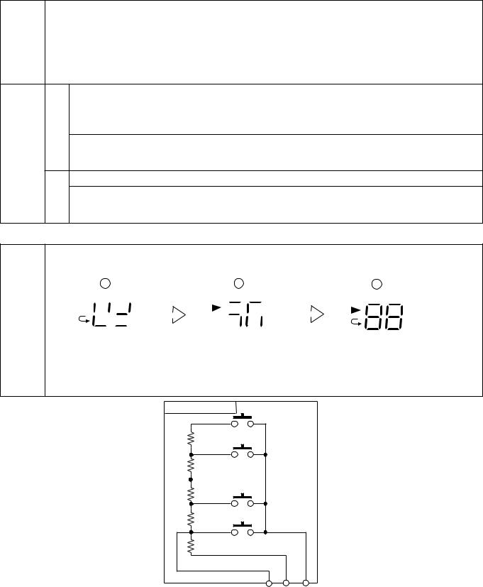
LCD MODE
Start |
While holding down the "STOP" button, move the FUNCTION/POWER switch to "CD". |
|||||||||||
Then, release the "STOP" button and, within 0.5 second, press the REVIEW/DOWN button. |
||||||||||||
|
||||||||||||
|
|
|
|
|
|
|
|
|
|
|
|
|
Display |
1 |
2 |
3 |
|
||||||||
|
|
|
|
|
|
|
|
|
|
|
|
|
|
|
|
|
|
|
|
|
|
|
|
|
|
|
|
|
|
|
|
|
|
|
|
|
|
|
|
|
|
|
|
|
|
|
|
|
|
|
|
|
|
|
|
|
|
|
|
|
|
|
|
|
1 second |
1 second |
*After the number 3has appeared in the display, each time the "UP/CUE" button is pressed, the display will switch in the following order: 1, 2, and then 3.
SWITCH PWB – A2
R771 |
SW774 |
|
TRACK DOWN/ |
|
|
3.9K |
REVIEW |
|
R772 |
SW773 |
|
2.7K |
TRACK UP/ |
|
TEST |
CUE |
|
POINT |
|
|
R773 |
|
|
1.8K |
|
|
|
SW771 |
|
R774 |
PLAY |
|
1.5K |
|
|
R776 |
SW7712 |
|
10K |
STOP |
|
|
+B |
|
|
3 |
1 |
TO CD SECTION
Figure 7
– 7 –
(1/2) DIAGRAM BLOCK 8 Figure – 8 –
24
27
28
31
34
35
36
|
|
|
|
|
|
|
|
|
|
CD LID |
|
|
|
|
|
|
|
|
|
|
OPEN/CLOSE |
|
|
|
|
|
|
|
|
|
|
SW761 |
|
|
|
|
|
|
|
|
|
CD |
|
|
|
|
|
|
|
|
OPERATION |
|
||
|
|
|
|
|
|
|
|
|
KEY |
|
|
|
|
|
|
|
SW771~SW774 |
|
|||
LCD701 |
|
RX771 |
|
|
|
|
|
|||
CD LCD |
REMOTE |
|
|
|
|
|
||||
|
|
SENSOR |
|
|
|
|
|
|||
|
|
|
3 2 1 |
|
|
|
|
PICKUP UNIT |
||
|
|
|
|
|
|
X701 |
|
|
||
|
|
|
|
|
|
4MHz |
|
|
||
57 ~ 60 |
41 ~ 44 |
30 |
33 |
22 |
|
|
23 |
|
||
SEG4 |
SEG1 |
COM3 |
COM0 |
RC IN |
K1 |
XIN |
|
XOUT |
|
|
|
|
|
|
|
|
|
|
LID 37 |
|
|
|
|
IC701 |
|
VLC3 38 |
|
|||||
|
IX0105AW |
|
|
|||||||
|
|
|
|
|
|
|
VDD 25 |
|
||
|
|
SYSTEM |
|
|
|
+5V |
FOCUS COIL |
|||
|
MICROCOMPUTER |
|||||||||
|
(D) |
|
||||||||
|
|
RES |
|
SL– |
DRF |
WRQ |
RESET |
SL+ 13 |
TRACKING COIL |
|
|
|
|
|
|
|
|
|
|||
|
|
|
|
|
|
|
|
|
||
|
|
|
|
|
|
|
|
SL– 14 |
|
|
|
|
9 |
~ 14 17 ~ 19 21 |
|
20 |
|
||||
|
LASER |
+5V |
|
|
|
|
|
DRIVER |
|
|
|
||
|
Q805 |
|
|
|
|
|
|
|
64 |
62 |
|
|
|
1 |
FIN2 |
VCC1 |
LDO |
|
|
|
2 |
FIN1 |
|
|
|
|
|
3 |
E |
|
|
|
|
|
4 |
F |
|
|
|
|
|
|
|
IC801 |
|
|
||
|
LA9240M |
|
|
|||
|
SERVO AMP. |
SLI |
44 |
|||
|
|
|
SLC |
43 |
||
|
|
|
CV+ |
40 |
||
|
TO FD SPO SLEO |
SLD |
THLD/DEF CLK CL DAT |
CE DRF |
~ |
|
30 |
32 |
|||||
SL– |
|
|
JP– |
|||
31 |
SL+ |
|
|
|
|
|
|
15 16 27 28 29 |
49 50 51 52 53 54 |
|
|||
|
XL801 |
+5V |
|
|
|
|
|
|
|
|
|
|
|
|
|
||
|
16.93MHz |
|
|
|
|
|
|
|
|
44 |
45 |
6 23 43 |
|
|
|
|
|
|
XOUT |
XIN |
VVDD VDD XVDD |
63 |
|
|
|
|
|
|
|
|
|
64 |
|
|
|
|
|
|
|
|
62 |
1 |
R-CH |
|
9 |
EFMO |
|
|
|
51 |
|
||
IC802 |
|
|
2 |
GND (A) |
TO |
|||
10 |
EFMIN |
|
|
|
||||
12 |
CLV+ |
LC78622E |
LCHO 37 |
3 |
L-CH |
MAIN |
||
13 |
CLV– |
SERVO/SIGNAL |
+7.4V |
4 |
+7.4V (D) |
SECTION |
||
|
||||||||
14 |
V/P |
CONTROL |
|
(CD) |
5 |
GND (D) |
|
|
15 |
HFL |
|
|
|
|
6 |
POWER GND |
|
16 |
TES |
|
|
|
46 |
|
||
|
|
|
|
|
|
|||
17 |
TOFF |
|
|
|
39 |
|
|
|
18 |
TGL |
|
|
|
38 |
|
|
|
19 |
JP+ |
|
|
|
33 |
|
|
|
20 |
JP– RES. CQCK. COIN |
|
32 |
|
|
|
||
|
SQOUT. RWC. WRQ |
|
|
|
|
|
||
|
1 61 58 57 56 55 54 53 |
2 4 |
8 11 |
|
|
|
|
|
CL, DAT, SELIAL CONTROL
|
|
|
|
|
CONSTANT |
|
|
|
|
|
|
VOLTAGE |
|
|
|
|
|
+5V |
REGULATOR |
|
|
|
|
|
|
|
|
|
|
|
|
Q804 |
|
|
|
|
|
|
3 10 19 23 25 |
|
|
|
|
|
1 |
IC804 |
|
|
|
M701 |
|
2 |
22 |
+7.4V |
|
PICKUP IN |
M |
11 |
BA5914FP |
|||
SPIN |
12 |
5 |
2 |
|||
|
|
|
|
|
||
SW702 |
MOTOR |
|
|
FOCUS/TRACKING |
|
|
|
|
6 |
|
|||
PU-IN SW |
|
|
17 |
|
||
|
|
|
18 |
/SPIN/SLIDE |
7 |
|
|
M702 |
M |
26 |
DRIVER |
8 |
|
|
SLIDE |
27 |
|
13 |
|
|
|
|
28 |
|
|||
|
MOTOR |
|
|
|
|
|
|
|
|
|
|
|
|
CD111/111C-QT

(2/2) DIAGRAM BLOCK 9 Figure – 9 –
FM ROD ANTENNA |
|
|
|
IC1 |
|
|
|
|
|
|
AM IF |
|
455kHz |
FM DET |
|
VR1 |
|
|
|
|
||
|
|
|
LA1186N |
|
T1 |
CF |
|
T3 |
|
CP |
T2 |
|
AM / FM VCO |
|
|
|
TUNER |
|||||
|
|
|
FM FRONT END |
7 |
FM IF |
10.7MHz |
|
|
|
SELECT |
|
|
|
|
+B |
|||||||
|
RF AMP |
|
|
|
|
|
|
|
|
|
|
|
+B |
|
|
|
|
|
|
|||
|
|
|
|
|
|
|
|
|
|
|
|
|
|
|
|
|
|
|
||||
F1 |
|
|
|
|
|
|
|
|
|
|
|
|
|
|
|
|
|
|
|
|||
1 |
|
MIX |
|
OSC |
|
|
|
|
|
|
|
|
|
|
|
|
|
|
|
|
||
B.P.F |
|
|
|
|
IC2 |
1 |
3 |
2 |
5 |
20 |
17 |
15 |
11 13 |
15 |
14 |
|
7 |
21 |
||||
|
|
|
VCC |
|
|
|
|
|
||||||||||||||
|
|
|
|
|
|
4 |
|
LA1805 |
|
|
|
|
|
|
|
|
|
|
|
|
VCC |
|
|
2 |
3 |
5 |
9 |
6 |
8 |
|
|
|
|
|
|
|
|
|
|
|
|
|
|||
|
|
FM / AM |
|
|
|
|
|
|
|
|
PILOT |
|
ST. |
|
||||||||
|
|
|
|
|
|
|
|
|
|
|
|
|
DET. |
POST |
|
|
TRIG. |
|
||||
|
|
|
|
|
|
|
|
|
IF MPX. |
|
|
FM - IF |
|
|
DET. |
DRIV. |
||||||
|
|
|
|
|
|
|
|
|
|
|
AMP. |
|
|
|||||||||
|
|
|
|
|
|
|
|
|
|
|
|
|
|
|
|
|
|
|
|
|
|
|
|
FM |
|
22 |
RF |
MPX |
LEVEL - DBT. |
MUTE |
|
|
|
FF |
|
L1 |
+B |
L2 |
|
|
|
|||||||
|
|
|
|
|||||||||
FM RF |
|
FM OSC |
|
|
|
AM - IF |
DET. |
|
PHASE |
VCO |
FF |
FF |
|
|
|
|
|
|
|
DET. |
|||||
|
|
|
|
|
|
|
|
TU |
|
|
|
|
|
|
|
23 |
REG. |
OSC |
|
AGC |
DRIV. |
DECODER |
|
ST. |
|
L3 |
|
|
|
|
|
|
|
|
|
|
SWIT. |
|
AM BAR ANT. |
|
|
|
|
|
GND |
|
|
|
|
|
|
FROM |
1 |
R-CH |
|
(AUDIO GND) |
|
||
CD |
|
||
SECTION |
2 |
L-CH |
CD |
|
3 |
+7.4V |
|
|
4 |
|
|
|
+B2 |
|
|
|
5 |
(DIGITAL GND) |
|
|
6 |
(POWER GND) |
|
|
|
|
REC / PB
|
SW102 |
|
|
C,E |
|
P.B |
P.B |
|
L-CH |
SW102 |
|
REC / PB |
||
REC / PB |
||
HEAD |
B.D |
|
R-CH |
|
|
ERASE |
|
|
HEAD |
SW102-H |
|
|
||
|
REC / PB |
POWER/
FUNCTION  RADIO
RADIO
SW201-A,B
|
TAPE |
EC / PB |
REC |
SW102 |
|
A,F |
|
P.B 5 L |
L |
1 P. B |
9 R |
R 12REC |
|
REC |
|
|
IC101 |
|
6 |
EQULIZER |
||
AMP. |
|
|
BA331IL |
|
8 |
REC
C201 |
+B1 |
|
L201 |
||
M601 |
||
|
BIAS |
SW102-G |
TAPE |
OSC. |
REC / PB |
MOTOR |
24 |
6 |
4 |
12 |
8 |
19 18 |
9 |
10 |
L5
AM OSC
X-BASS VOLUME
SW202
A,B VR201
A,B
STANBY
VOLTAGE
REGULATOR
|
IC203 |
+B1 |
|
KIA7808P |
|
|
SW201-C |
|
|
|
|
|
|
POWER/ |
|
|
FUNCTION |
SW201-D |
+B2 |
AM / FM |
|
||
|
SELECT |
|
POWER / |
|
|
|
+B |
|
FUNCTION |
|
|
|
FM +B |
|
|
|
D651~D654
RECTIFIER
SW601
MAIN
IC501
LA4597
POWER AMP.
2 L |
|
12 |
6 R |
|
10 |
5 |
11 |
8 |
T651 POWER
TRANSFORMER
SP501
L-CH
SPEAKERS
SP502
R-CH
SO651
AC INPUT
AC 120V 60Hz
|
|
|
|
|
BATTERY |
|
|
|
|
||
TUNER |
|
|
|
|
DC12V |
+B |
|
|
[' D' SIZE (UM/SUM-1, |
||
|
R20 or HP-2)BATTERYx8] |
||||
CD111/111C-QT

QT-CD111/111C
A
B
C
D
E
F
G
H
|
IC701 |
|
|
|
|
|
|
|
|
|
|
|
|
|
|
|
|
|
|
|
|
|
|
|
|
|
|
|
|
|
|
|
|
|
|
|
|
|
|
|
|
|
|
|
|
|
|
|
|
|
|
|
|
|
|
|
|
|
|
PIN |
VOLTAGE |
PIN |
VOLTAGE |
|
|
|
|
|
|
|
|
|
|
|
|
|
|
|
|
|
|
|
|
|
|
|
|
|
|
|
|
|
|
|
|
|
|
|
|
|
|
|
|
|
|
|
|
|
|
|
|
|
|
|
|
|
|
||
NO. |
NO. |
|
|
|
|
|
|
|
|
|
|
|
|
|
|
|
|
|
|
|
|
|
|
|
|
|
|
|
|
|
|
|
|
|
|
|
|
|
|
|
|
|
|
|
|
|
|
|
|
|
|
|
|
|
|
||||
1 |
0V |
33 |
5V |
|
|
|
|
|
|
|
|
|
|
|
|
|
|
|
|
|
|
|
|
|
|
|
|
|
|
|
|
|
|
|
|
|
|
|
|
|
|
|
|
|
|
|
|
|
|
|
|
|
|
|
|
|
|
|
|
2 |
0V |
34 |
0V |
|
|
|
|
|
SWITCH PWB-A2 |
|
|
|
|
|
|
|
|
|
|
|
|
|
|
|
|
|
|
|
|
|
|
|
|
|
|
|
|
|
|
|
|
|
|
|
|
|
|
|
|
||||||||||
3 |
0V |
35 |
0V |
|
|
|
|
|
|
|
|
|
|
|
|
|
|
|
|
|
|
|
|
|
|
|
|
|
|
|
|
|
|
|
|
|
|
|
|
|
|
|
|
|
|
|
|
|
|||||||||||
4 |
0V |
36 |
0V |
|
|
|
|
|
|
|
|
|
|
|
|
|
|
|
|
|
|
|
|
|
|
|
|
|
|
|
|
|
|
|
|
|
|
|
|
|
|
|
|
|
|
|
|
|
|||||||||||
5 |
0V |
37 |
0.4V |
|
|
|
|
|
|
|
|
|
|
|
|
|
|
|
|
|
|
|
|
|
|
|
|
|
|
|
|
|
|
|
|
|
|
|
|
|
|
|
|
|
|
|
|
|
|
|
|
|
|
|
|
|
|
|
|
6 |
0V |
38 |
5V |
|
|
|
|
|
|
SW774 |
|
|
|
|
|
|
|
|
|
|
|
|
|
|
|
|
|
|
|
|
|
|
Q805 |
|
|
|
|
|
|
|
|
|
|
|
|
|
|
|
|
|
|
|
|
|
|
||||
7 |
3.9V |
39 |
3.1V |
|
|
|
|
|
TRACK DOWN/ |
|
|
|
|
|
|
|
|
|
|
|
|
|
|
|
|
|
|
|
|
|
|
|
|
|
|
|
|
|
|
|
|
|
|
|
|
|
|
|
|
|
|||||||||
8 |
0V |
40 |
1.5V |
|
|
|
|
|
REVIEW |
|
|
|
|
|
|
|
|
|
|
|
|
|
|
|
|
|
|
|
|
SS9012H |
|
|
|
|
|
|
|
|
|
|
|
|
|
|
|
|
|
|
|
|
|
|
|||||||
9 |
5V |
41 |
2.4V |
|
|
R771 |
3.9K |
|
|
|
|
|
|
|
|
|
|
|
|
|
|
|
|
|
|
|
|
|
|
|
|
+B |
|
|
|
|
|
|
|
|
|
|
|
|
|
|
|
|
|
|
|
|
|
|
|
|
|
||
10 |
4.1V |
42 |
2.4V |
|
|
|
SW773 |
|
|
|
|
|
|
|
|
|
|
|
|
|
|
|
|
|
|
|
|
|
|
|
|
|
|
|
|
|
|
|
|
|
|
|
|
|
|
|
|
|
|
|
|
|
|
||||||
11 |
4.1V |
43 |
2.4V |
|
|
|
|
|
|
|
|
|
|
|
|
|
|
|
|
|
|
|
|
|
|
R842 |
|
|
|
|
|
|
|
|
|
|
|
|
|
|
|
|
|
|
|
|
|
|
|
|
|
|
|
||||||
12 |
0V |
44 |
2.4V |
|
|
|
|
TRACK UP/ CUE |
|
|
|
|
|
|
|
|
|
|
|
|
|
|
|
|
|
|
|
|
|
C849 |
|
|
|
|
|
|
|
|
|
|
|
|
|
|
|
|
|
|
|
||||||||||
13 |
0V |
45 |
2.4V |
|
|
R772 |
|
|
|
|
|
|
|
|
|
|
|
|
|
|
|
|
|
|
|
|
|
|
|
22 |
|
|
|
|
|
|
|
|
|
|
|
|
|
|
|
|
|
|
|
|
|
|
|
|
|||||
|
|
2.7K |
|
|
|
|
|
|
|
|
|
|
|
|
|
|
|
|
|
|
|
|
|
|
|
|
|
|
|
0.022 |
|
|
|
|
|
|
|
|
|
|
|
|
|
|
|
|
|
|
|
||||||||||
15 |
0.4V |
47 |
2.4V |
|
|
|
|
|
|
|
|
|
|
|
|
|
|
|
|
|
|
|
|
|
|
|
|
|
|
|
|
|
|
|
|
|
|
|
|
|
|
|
|
|
|
|
|
|
|
|
|
|
|
||||||
14 |
0V |
46 |
2.4V |
|
|
|
|
|
|
|
|
|
|
|
|
|
|
|
|
|
|
|
|
|
|
|
|
|
|
|
|
|
|
|
|
|
|
|
|
|
|
|
|
|
|
|
|
|
|
|
|
|
|
|
|
|
|
|
|
16 |
0.4V |
48 |
2.4V |
|
|
R773 |
2.7K |
|
SW771 |
|
|
|
|
|
|
|
|
|
|
|
|
|
|
|
|
|
|
|
|
C848 |
|
|
|
|
|
|
|
|
|
|
|
|
|
|
|
|
|
|
|
|
|
|
|
||||||
17 |
0V |
49 |
2.4V |
|
|
|
PLAY/ |
|
|
|
|
|
|
|
|
|
|
|
|
|
|
|
|
|
|
|
|
1/50 |
|
|
|
|
|
|
|
|
|
|
|
|
|
|
|
|
|
|
|
|
|
|
|
|
|||||||
18 |
0V |
50 |
2.4V |
|
|
|
|
|
REPEAT |
|
|
|
|
|
|
|
|
|
|
|
|
|
|
|
|
|
|
|
|
|
|
|
|
|
|
|
|
|
|
|
|
|
|
|
|
|
|
|
|
|
|
|
|
|
|||||
19 |
0V |
51 |
2.4V |
|
|
|
|
|
|
|
|
|
|
|
|
|
|
|
|
|
|
|
|
|
|
|
|
|
|
|
+B |
|
|
|
|
|
|
|
|
|
|
|
|
|
|
|
|
|
|
|
|
|
|
|
|
|
|
|
|
20 |
0V |
52 |
2.4V |
|
|
R774 2.7K |
|
STOP |
|
|
|
|
|
|
|
|
|
|
CD LID |
|
|
|
|
|
|
|
|
|
|
|
|
|
|
|
|
|
|
|
|
|
|
|
|
|
|
|
|
|
|
|
|
|
|
|
|||||
22 |
2.5V |
54 |
2.4V |
|
|
|
|
|
|
|
|
|
|
|
|
|
|
|
|
|
|
|
|
|
|
|
|
|
|
|
|
|
|
|
|
|
|
|
|
|
|
|
|
|
|
|
|
|
|
|
|
|
|||||||
21 |
5V |
53 |
2.4V |
|
|
|
|
|
SW772 |
|
|
|
|
|
|
|
|
|
SW761 |
|
|
|
|
|
|
|
|
|
|
|
|
|
|
|
|
|
|
|
|
|
|
|
|
|
|
|
|
|
|
|
|
|
|
|
|
||||
23 |
2.5V |
55 |
2.4V |
|
|
|
|
10K |
|
|
|
|
|
|
+B |
|
|
|
|
|
OPEN/CLOSE |
|
|
|
|
|
|
|
|
|
|
|
|
0.33/50 |
1/50 |
0.01 |
|
10/16 |
|
0.1/50 |
|
|
|
|
|
|
|
|
|
|
|
|
|
|
|||||
25 |
5V |
57 |
2.4V |
|
|
|
|
|
|
|
|
|
|
|
|
|
|
|
|
|
|
|
|
|
|
|
|
|
|
|
|
|
|
|
|
|
|
|
|
|
|
|
|
|
|
|
|
|
|||||||||||
24 |
0V |
56 |
2.4V |
|
|
|
|
R776 |
|
|
|
|
|
|
|
|
|
|
|
|
|
|
|
|
|
|
|
|
|
|
|
|
|
|
|
|
|
|
|
|
|
|
|
|
|
|
|
|
|
|
|
|
|
|
|
|
|||
26 |
5V |
58 |
2.4V |
|
|
|
|
|
|
|
|
|
|
|
|
|
|
|
|
|
|
|
|
|
|
|
|
|
|
|
|
|
|
|
|
C840 |
C839 |
C838 |
|
837C |
|
835C |
|
|
|
|
|
|
|
|
|
|
|
|
|
|
|||
27 |
0V |
59 |
2.4V |
|
|
|
|
|
|
|
|
|
|
|
|
|
|
|
|
|
|
|
|
|
|
|
|
|
|
|
|
|
|
|
|
|
|
|
|
|
|
|
|
|
|
|
|
|
|
|
|
||||||||
28 |
0V |
60 |
2.4V |
|
|
|
|
|
|
|
|
|
|
|
|
|
|
|
|
|
|
|
|
|
|
|
|
|
|
|
|
|
|
|
|
|
|
|
|
|
|
|
|
|
|
|
|
|
|
|
|
|
|
|
|
|
|
|
|
29 |
5V |
61 |
2.4V |
|
|
|
|
|
|
|
|
|
|
|
|
|
|
|
|
|
|
|
|
|
|
|
|
|
|
|
|
|
|
|
|
|
|
|
|
|
|
|
|
|
|
|
|
|
|
|
|
|
|
|
|
|
|
|
|
30 |
4.8V |
62 |
0V |
|
|
|
|
|
|
|
|
|
|
|
|
|
|
|
|
|
|
|
|
|
|
|
|
|
|
|
|
|
|
|
|
|
|
|
|
|
|
|
|
|
|
|
|
|
|
|
|
|
|
|
|
|
|
|
|
31 |
0V |
63 |
0V |
|
|
|
|
|
|
|
|
|
|
|
|
|
3 |
|
|
1 |
|
|
|
|
|
|
|
|
|
|
|
|
|
|
|
|
|
|
|
|
|
|
|
|
|
|
|
|
|
|
|
|
|
|
|
|
|
|
|
32 |
3.8V |
64 |
0V |
|
|
|
|
|
|
|
|
|
|
|
|
|
|
|
|
|
|
|
|
|
|
|
|
|
|
|
|
|
|
|
|
|
|
|
|
|
|
|
|
|
|
|
|
|
|
|
|
|
|
|
|
|
|
|
|
|
|
|
|
|
|
|
|
|
|
|
|
|
|
|
|
|
|
|
|
FW701 |
|
|
|
|
|
|
|
|
|
|
|
|
|
|
|
|
|
|
|
|
|
|
|
|
|
|
|
|
|
|
|
|
|
|
R871 |
|
|||
|
|
|
|
|
|
|
|
|
|
|
|
|
|
|
|
|
|
|
|
|
|
|
|
|
|
|
|
|
|
|
|
64 |
|
63 |
62 |
61 |
60 |
59 |
58 |
|
57 |
56 55 |
54 53 |
52 |
51 |
50 |
49 |
4.7K |
|
||||||||||
|
|
|
|
|
|
|
|
|
|
|
|
|
|
|
|
|
|
|
|
1 |
|
|
|
|
|
|
|
|
|
|
|
|
|
|
|
C845 |
|||||||||||||||||||||||
|
|
|
|
|
|
|
|
|
|
|
|
|
|
|
|
|
3 |
|
|
|
|
|
|
|
|
|
|
|
|
1 |
VCC1 |
|
LDS |
LDD |
BH1 |
PH1 |
LF2 |
|
VR |
|
REFI |
|
VCC2 |
FSS |
DRF CE |
DAT |
CL |
|
CLK |
DEF |
|
|
|||||||
|
|
|
|
|
|
|
|
|
|
|
|
|
|
|
|
|
|
|
|
|
|
|
|
|
|
|
|
|
|
|
|
|
|
|
|
48 NC |
4.7/50 |
||||||||||||||||||||||
|
|
|
|
|
|
|
|
|
|
|
|
|
|
|
|
|
|
|
|
|
|
|
|
|
|
|
|
|
|
|
|
|
|
|
|
|
|
|
|
|
|
|
|
|
|
|
|
|
|
|
|
|
|
|
|
||||
|
|
|
|
|
|
|
|
|
|
|
|
|
|
|
|
|
|
|
|
|
|
|
|
|
|
|
|
|
|
|
2 |
|
|
|
|
|
|
|
|
|
|
|
|
|
|
|
|
|
|
|
|
|
|
|
|
TBC 47 |
|
|
|
|
|
|
|
|
|
|
|
|
|
|
|
|
|
|
|
|
|
|
|
|
|
|
|
|
|
|
C803 |
|
|
3 |
E |
|
|
|
|
|
1 FIN2 |
|
|
|
|
|
|
|
|
|
|
|
|
|
|
|
FSC 46 |
|
|
||||
|
|
|
|
|
|
|
|
|
|
|
|
|
|
|
|
|
|
|
|
|
|
|
|
|
|
|
0.1/50 |
R803 |
4 |
F |
|
|
|
|
|
2 |
FIN1 |
|
|
|
|
|
|
|
|
|
|
|
|
|
|
|
GND 45 |
|
|
||||
|
|
|
|
|
|
|
|
|
|
|
|
|
|
|
|
|
|
|
|
|
|
|
|
|
|
|
|
|
5 |
TB |
|
|
|
|
|
|
|
|
|
|
|
|
|
|
|
|
|
|
|
|
|
|
|
SLI 44 |
|
|
|||
|
|
|
|
|
|
|
|
|
|
|
|
|
|
|
|
|
|
|
|
|
|
|
|
|
|
|
|
|
15K |
|
|
|
|
|
|
|
|
|
|
|
|
|
|
|
|
|
|
|
|
|
|
|
|
C834 |
|||||
|
|
|
|
|
|
|
|
|
|
|
|
|
|
|
|
|
|
|
|
|
|
|
|
|
|
|
|
R802 |
6 |
TE– |
|
|
|
|
|
|
|
|
|
|
|
|
|
|
|
|
|
|
|
|
|
|
|
|
|
||||
|
|
|
|
|
|
|
|
|
|
|
|
|
|
|
|
|
|
|
|
|
|
|
|
|
|
|
|
|
|
|
|
|
|
|
|
|
|
|
|
|
|
|
|
|
|
|
|
|
|
|
|
|
|
|
|||||
|
|
|
|
|
|
|
|
|
|
|
|
|
|
|
|
|
|
|
|
|
|
|
|
|
|
|
|
|
|
|
|
|
|
|
|
|
|
|
|
|
|
|
|
|
|
|
|
|
|
|
|
|
|
|
0.033 |
||||
|
|
|
|
|
|
|
|
|
|
|
|
|
|
|
|
|
|
|
|
|
|
|
|
|
|
C804 |
|
100K |
|
|
|
TE |
|
|
|
|
|
|
|
|
|
|
|
|
|
|
|
|
|
|
|
|
|
|
|
|
|
C833 |
|
|
|
|
|
|
|
|
|
|
|
|
|
|
|
|
|
|
|
|
|
|
|
|
|
|
|
|
|
|
|
7 |
|
|
|
|
|
|
|
|
|
|
|
|
|
|
|
|
|
|
|
|
|
|
|
|
|
|
|||
|
|
|
|
|
|
|
|
|
|
|
|
|
|
|
|
|
|
|
|
|
|
|
|
|
|
0.001 |
R804 |
C805 |
|
|
|
|
|
|
|
|
|
|
|
|
|
|
|
|
|
|
|
|
|
|
|
|
|
|
|
|
|||
|
|
|
|
|
|
|
|
|
|
|
|
|
|
|
|
|
|
|
|
|
|
|
|
|
|
|
|
|
|
|
|
|
|
|
|
|
|
IC801 |
|
|
|
|
|
|
|
|
|
0.001 |
R833 |
||||||||||
|
LCD701 |
|
|
|
|
|
|
|
|
|
|
|
|
|
|
|
|
|
|
|
|
|
|
|
|
2.2K |
0.033 |
|
|
8 |
TESI |
|
|
|
|
|
|
|
|
|
|
|
|
|
|
SLC |
43 |
|
|||||||||||
|
|
|
|
|
|
|
|
|
|
|
|
|
|
|
|
|
|
|
|
|
|
|
|
|
|
|
|
|
|
|
|
|
|
|
|
|
|
|
|
|
|
5.6K |
|||||||||||||||||
|
|
|
|
|
|
|
|
|
|
|
|
|
|
|
|
|
|
|
|
|
|
+B |
|
|
|
C807 |
|
C806 |
|
|
9 |
SCI |
|
|
|
|
|
LA9241M |
|
|
|
|
|
|
RFS– |
42 |
C830 |
R832 |
|||||||||||
|
|
|
|
|
|
|
|
|
|
|
|
|
|
|
|
|
|
|
|
|
|
|
|
|
|
|
|
|
|
|
|
|
|
|
|
|
|
|
|
|
|
|
|||||||||||||||||
|
|
|
|
|
|
|
|
|
|
|
|
|
|
|
|
|
|
|
|
|
|
|
|
|
|
0.1/50 R805 |
0.033 |
|
|
|
|
|
|
|
|
|
SERVO AMP. |
|
|
|
|
|
|
|
|
2P |
|||||||||||||
|
|
|
|
|
|
|
|
|
|
|
|
|
|
|
|
|
|
|
|
|
|
|
|
|
|
|
6.8K |
R806 |
|
|
|
TH |
|
|
|
|
|
|
|
|
|
RFSM 41 (CH) |
56K |
||||||||||||||||
|
|
|
|
|
|
|
|
|
|
|
|
|
|
|
|
|
|
|
|
|
|
|
|
|
|
|
|
|
|
10 |
|
|
|
|
|
|
|
|
|
|
|
|
|
|
|
|
|
|
|
|
|
|
|
|
|
|
|||
|
|
|
|
|
|
|
|
|
|
|
|
|
|
|
|
|
|
|
|
|
|
|
|
|
|
|
|
100 |
|
|
|
|
|
|
|
|
|
|
|
|
|
|
|
|
|
|
|
|
|
|
|
|
CV+ 40 |
|
|
||||
|
|
|
|
|
|
|
|
|
|
|
|
|
|
|
|
|
|
|
|
|
|
|
|
|
|
R807 |
C808 |
11 |
TA |
|
|
|
|
|
15 TO |
|
|
|
|
|
|
|
|
34 TGL |
|
|
|
|
|
|
|
||||||||
8 |
7 6 5 |
4 |
3 |
2 |
1 |
|
C701 0.022 C702 0.022 |
|
R708 |
|
|
|
|
|
|
|
|
|
|
|
|
1K |
C809 |
0.068 |
12 |
TD– |
|
|
|
|
16 FD |
|
|
|
|
|
|
|
|
33 JP+ |
|
|
|
|
|
CV– 39 |
|
|
|||||||||||
|
|
1K |
R710 |
|
1K |
|
|
|
|
|
|
|
C810 |
|
|
|
|
|
|
|
|
|
|
|
|
|
|
|
|
|
HFL |
37 |
|
||||||||||||||||||||||||||
|
|
|
|
|
|
|
|
|
|
|
|
|
|
|
|
|
|
R809 |
|
|
|
|
|
|
|
|
|
|
|
|
|
|
|
|
|
|
|
|
|
|
|
|
|||||||||||||||||
|
|
|
|
|
|
|
|
|
|
|
|
|
|
|
|
|
|
R709 |
|
|
|
|
|
|
|
|
0.047 |
|
|
|
|
|
|
|
|
|
|
|
|
|
|
|
|
|
|
|
|
|
|
|
SLOF |
38 |
|
|
|||||
|
|
|
|
|
|
|
|
|
|
|
|
|
|
|
|
|
|
|
|
|
|
|
|
|
|
|
|
|
|
|
|
|
|
|
|
|
|
|
|
|
|
|
|
|
|
|
|
|
|
|
|
|
|
|
|
|
|
|
|
|
|
|
|
|
|
|
|
|
|
|
|
|
|
|
10K |
|
|
|
|
|
|
|
|
|
|
27K |
R808 |
180P |
|
TD |
|
|
|
|
|
|
|
|
|
|
|
|
|
|
|
|
|
|
|
|
|
|
TES 36 |
|
|
||||
|
|
|
|
|
|
|
|
|
|
|
|
|
|
|
|
R711 |
|
|
|
|
|
|
|
|
|
|
12K |
|
|
13 |
|
|
|
|
|
|
|
|
|
|
|
|
|
|
|
|
|
|
|
|
|
|
|
|
|
|
|||
|
|
|
|
|
|
|
|
|
|
|
|
|
|
|
|
|
|
|
|
|
|
|
|
|
|
|
|
|
JP |
|
|
|
|
|
|
|
|
|
|
|
|
|
|
|
|
|
|
|
|
|
|
TOFF 35 |
|
|
|||||
|
|
|
|
|
|
|
|
|
|
|
|
|
|
|
|
2.7K |
|
|
|
|
|
|
|
|
|
R811 |
|
|
|
14 |
|
|
|
|
|
|
|
|
|
|
|
|
|
|
|
|
|
|
|
|
|
|
|
|
|
34 |
|
|
|
|
|
|
|
|
|
|
|
|
|
|
|
|
|
|
|
|
|
|
|
|
|
|
|
|
|
|
|
|
|
|
|
|
|
|
AGND NC |
|
|
|
|
|
|
|
|
|
|
|
|
|
|
|
|
|
|
||||||
|
|
|
|
|
|
|
|
|
|
|
|
|
|
|
|
|
|
|
|
|
|
|
|
|
|
|
3.3K |
|
|
|
15 |
FD– |
FA |
FA– |
FE |
FE– |
SP |
SPG |
|
SP– |
|
|
SPD SLEQ |
|
SLD |
|
SL– |
SL+ JP– |
33 |
|
|
||||||||
|
|
|
|
|
|
|
|
|
|
|
|
|
|
|
|
|
|
|
|
|
|
|
|
|
|
|
|
|
|
|
16 |
|
|
|
|
|
|
|
|
||||||||||||||||||||
|
|
50 |
SEG11 |
|
|
|
|
|
|
|
|
|
|
P3P40 |
33 |
31 |
|
|
R714 |
|
|
|
|
|
|
|
|
|
17 18 |
19 20 |
21 |
22 23 |
24 |
25 26 |
C816 |
0.001 |
27 28 |
29 |
|
30 31 32 |
|
|
|||||||||||||||||
|
|
|
48 |
47 |
46 45 44 43 42 41 40 39 38 37 36 35 34 |
|
|
|
|
|
+B |
|
|
|
|
R813 |
|
|
|
|
C812 |
|
|
|
|
R820 |
|
|
|
|
|
|
|
|
|
|
|
|
|
|
|
|
|||||||||||||||||
|
|
|
|
|
|
|
|
|
|
|
|
|
|
|
|
|
|
|
|
10K |
|
|
|
|
|
|
|
|
|
|
|
|
|
|
|
|
|
|
|
|
|
|
|
|
|
|
|
|
|
|
|||||||||
|
|
49 SEG12 |
|
SEG16 |
COM0 COM1 |
COM2 COM3 |
VLC1 |
VLC2 |
VLC3 |
KIDSW AIN7 |
SIMUKE AIN6 |
AIN5 |
VREFP33 |
32 |
|
|
|
|
|
|
|
|
|
|
|
|
330P |
|
|
|
|
|
|
|
|
|
|
|
|
|
|
|
|
|
|
|
|
||||||||||||
|
|
|
|
|
|
|
|
|
|
|
|
|
|
|
33K |
|
|
|
|
|
|
|
|
10K |
|
|
|
R824 |
|
|
|
|
|
|
|
|
|
|
|||||||||||||||||||||
|
|
52 |
SEG9 |
|
29 |
|
|
C705 |
|
|
|
|
|
|
R828 |
R812 C813 |
R814 |
10K |
|
82K |
|
|
C815 |
|
R821 56K |
10K 819C |
47/16 |
C820 |
.00330 |
|
|
|
|
|
|
||||||||||||||||||||||||
|
|
54 |
SEG7 |
|
31 |
P31 |
XCIN |
27 |
|
|
|
|
|
|
|
|
|
R829 |
|
|
|
|
|
|
|
|
0.0047 |
|
R822 |
|
|
|
|
|
|
||||||||||||||||||||||||
|
|
|
|
|
|
|
|
|
|
|
|
|
|
|
|
|
|
|
|
C704 |
|
|
|
|
|
|
|
|
|
|
|
|
|
|
|
|
|
|
|
|
|
|
|
|
|
|
|
|
|
|
|
|
|
|
|
|
|
|
|
|
|
51 SEG10 |
|
|
|
|
|
|
|
|
|
|
|
|
30 |
|
|
100/10 |
|
|
|
|
|
|
|
|
|
|
|
|
|
R817 |
|
|
|
|
|
|
|
|
|
|
|
|
|
|
|
|
|
|
|
|
|
|
|||||
|
|
53 |
SEG8 |
|
|
|
|
|
|
32 P32 |
|
AVSS 28 |
|
|
|
|
|
|
|
|
|
|
1K |
|
15K |
0.1 |
|
|
|
|
|
|
|
|
|
|
|
|
|
|
|
|
|
|
|
1.2K R826 220K |
|
|
|
|
|
||||||||
|
|
|
|
|
|
|
|
|
|
|
|
|
|
4MHz |
|
|
|
22K |
|
|
|
|
|
|
|
|
|
|
R819 |
39K |
|
R823 1.2K |
|
C817 0.47/50 |
R830C818 |
1K 1/50 |
R825 |
|
R827 220K |
|
|
||||||||||||||||||
|
|
59 SEG2 |
|
MICROCOMPUTER |
|
XIN 22 1K |
|
|
|
|
|
|
|
|
1K |
|
|
|
|
|
|
|
|
|
|
|
|
|
|
||||||||||||||||||||||||||||||
|
|
55 |
SEG6 |
|
|
|
IC701 30 P30 |
XCOUT 26 |
|
|
0.022 |
|
|
|
|
|
GND |
R839 |
|
|
|
R815 C814 R816 |
|
|
|
|
|
|
|
|
|
|
|
|
|
|
|
|
|
|
|
|
|
||||||||||||||||
|
|
56 |
SEG5 |
|
|
IX0105AW |
|
|
|
VDD 25 |
|
|
|
|
|
|
|
|
|
|
22K |
|
VREF |
|
|
|
|
|
|
|
|
|
|
|
|
|
|
|
|
|
|
|
|
|
|||||||||||||||
|
|
57 SEG4 |
|
|
SYSTEM |
|
|
|
VSS |
24 |
|
|
|
|
|
|
|
|
|
|
|
|
|
|
|
|
|
|
|
|
|
|
|
|
|
|
|
|
|
|
|
|
|
|
|
|
|
|
|
|
|
|
|||||||
|
|
58 |
SEG3 |
|
|
|
|
|
XOUT |
23 R713 |
|
|
|
X701 |
|
|
|
R840 |
|
|
|
|
|
|
|
|
|
|
|
|
|
|
|
|
|
|
|
|
|
|
|
|
|
|
|
|
|
|
|
|
|||||||||
|
|
|
|
|
|
|
|
|
|
|
|
|
|
|
|
|
|
|
|
|
|
|
|
|
|
|
|
|
|
|
|
|
|
|
|
|
|
|
|
|
|
|
|
|
|
|
|
|
|
||||||||||
|
|
60 SEG1 |
POWERIN |
|
|
18 SQOUT P21 |
|
RESET 21 |
R730 1K |
|
|
|
|
|
|
C811 |
|
|
|
|
|
|
|
|
|
|
|
|
|
|
|
|
|
|
|
|
|
|
|
|
|
R831 |
1K |
|
|
|
|
|
|
||||||||||
|
|
61 |
|
P10 |
|
|
MUTED1 |
RESD3 |
COCKD4 |
COIND5 |
RWCD6 |
SL+D7 SL–D8 |
|
|
20 |
|
|
|
|
|
|
|
|
|
|
|
|
|
|
|
|
|
|
|
|
|
|
|
|
|
|
|
|
|
|
|
|
|
|
|
|
|
|||||||
|
|
SEG0 |
|
|
|
17 DFR P20 |
|
PU-IN P23 |
|
|
|
|
|
R736 |
|
|
|
|
|
|
|
|
|
|
|
|
|
|
|
|
|
|
|
|
|
|
|
|
|
|
|
|
|
|
|
|
|
|
|
||||||||||
|
|
62 |
P00 |
|
|
|
|
|
|
|
|
|
|
WRQ P22 |
19 |
|
|
|
|
|
1K |
|
|
|
|
|
|
|
|
|
|
|
|
|
|
|
|
|
|
|
|
|
|
|
|
|
|
|
|
|
|
|
|
|
|
|
|
||
|
|
63 P01 |
|
|
|
|
|
|
|
|
|
|
|
|
|
18 |
|
|
|
|
|
|
|
|
|
|
|
|
|
|
|
|
|
|
|
|
|
|
|
|
|
|
|
|
|
|
|
|
|
|
|
|
|
|
|
|
|
|
|
|
|
64 |
P02 |
|
|
|
|
|
|
|
|
|
|
|
|
|
17 |
|
|
|
|
|
R715 |
|
|
|
|
|
|
|
|
|
|
|
|
|
|
|
|
|
|
|
|
|
|
|
|
|
|
|
|
|
|
|
|
|
|
|
|
|
|
|
|
|
|
|
|
|
|
|
|
|
|
|
|
|
|
|
|
R727 |
|
|
|
|
|
|
|
|
|
|
|
|
|
|
|
|
|
|
|
|
|
|
|
|
|
|
|
|
|
|
|
|
|
|
|
|
|
||
|
|
|
1 |
2 |
3 |
4 |
5 6 |
7 8 |
9 10 11 12 13 14 15 16 |
|
|
|
|
15K |
|
|
|
|
|
|
|
|
|
|
|
|
|
|
|
|
|
|
|
|
|
|
|
|
|
|
|
|
|
|
|
|
|
|
|
|
|||||||||
|
|
|
R734 1K |
|
|
1K |
|
|
|
|
|
|
|
|
|
|
|
|
|
|
|
|
|
|
|
|
|
|
|
|
|
|
|
|
|
|
|
|
|
|
|
|
|
|
|
||||||||||||||
|
|
|
|
|
|
|
|
|
|
|
|
|
|
|
|
|
|
|
|
|
|
|
|
|
|
|
|
|
|
|
|
|
|
|
|
|
|
|
|
|
|
|
|
|
|
|
|
|
|
|
|
|
|
|
|
|
|
||
|
|
|
|
|
|
|
|
|
|
|
|
|
|
|
|
|
|
|
|
|
|
|
|
|
|
|
|
|
|
|
|
|
|
|
|
|
|
|
|
|
|
|
|
|
|
|
|
|
|
|
|
|
|
|
|
|
|
|
|
|
|
|
|
|
|
|
|
|
|
|
|
|
|
|
|
|
|
|
|
|
|
|
|
|
+B |
5V |
|
|
|
|
|
|
|
|
|
|
|
|
|
|
|
|
|
|
|
|
|
|
|
|
|
|
|
|
|
|
|
|
|
|
|
|
|
|
|
|
|
|
|
|
|
|
|
|
|
R726 1K |
|
|
|
|
|
|
|
DIGITAL GND |
|
|
|
|
|
|
|
|
|
|
|
|
|
|
|
|
|
|
|
|
|
|
|
|
|
|
|
|
|
|
|
||||
|
|
|
|
|
|
|
|
|
|
|
|
|
|
|
|
R728 1K |
|
|
|
|
|
|
|
PU IN |
|
|
|
|
|
|
|
|
|
|
|
|
|
|
|
|
|
|
|
|
|
|
|
|
|
|
|
|
|
|
|
|
|||
|
|
|
|
|
|
|
|
|
|
|
|
|
|
|
|
R729 1K |
|
|
|
|
|
|
|
WRQ |
|
|
|
|
|
|
|
|
|
|
|
|
|
|
|
|
|
|
|
|
|
|
|
|
|
|
|
|
|
|
|
|
|||
|
|
|
|
|
|
|
|
|
|
|
|
|
|
|
|
R731 1K |
|
|
|
|
|
|
|
SQOUT |
|
|
|
|
|
|
|
|
|
|
|
|
|
|
|
|
|
|
|
|
|
|
|
|
|
|
|
|
|
|
|
|
|||
|
|
|
|
|
|
|
|
|
|
|
|
|
|
|
|
R732 1K |
|
|
|
|
|
|
|
DRF |
|
|
|
|
|
|
|
|
|
|
|
|
|
|
|
|
|
|
|
|
|
|
|
|
|
|
|
|
|
|
|
|
|||
|
|
|
|
|
|
|
|
|
|
|
|
|
|
|
|
R733 1K |
|
|
|
|
|
|
|
SL– |
|
|
|
|
|
|
|
|
|
|
|
|
|
|
|
|
|
|
|
|
|
|
|
|
|
|
|
|
|
|
|
|
|||
|
|
|
|
|
|
|
|
|
|
|
|
|
|
|
|
|
|
|
|
|
|
|
|
|
|
SL+ |
|
|
|
|
|
|
|
|
|
|
|
|
|
|
|
|
|
|
|
|
|
|
|
|
|
|
|
|
|
|
|
|
|
|
|
|
|
|
|
|
|
|
|
|
|
|
|
|
|
|
|
|
|
|
|
|
|
|
|
RWC |
|
|
|
|
|
|
|
|
|
|
|
|
|
|
|
|
|
|
|
|
|
|
|
|
|
|
|
|
|
|
|
|
|
|
|
|
|
|
|
|
|
|
|
|
|
|
|
|
|
|
|
|
|
|
|
+B |
|
|
|
CO IN |
|
|
|
|
|
|
|
|
|
|
|
|
|
|
|
|
|
|
|
|
|
|
|
|
|
|
|
|
|
|
|
|
|
|
|
|
|
|
|
|
|
|
|
|
|
|
|
|
|
|
|
|
|
|
|
|
|
|
CQCK |
|
|
|
|
|
|
|
|
|
|
|
|
|
|
|
|
|
|
|
|
|
|
|
|
|
|
|
|
|
|
|
|
||
|
|
|
|
|
|
|
|
|
|
|
|
|
|
|
|
|
|
|
|
|
|
|
|
|
|
|
|
|
|
|
|
|
|
|
|
|
|
|
|
|
|
|
|
|
|
|
|
|
|
|
|
|
|
|
|
|
|
||
|
|
|
|
|
|
|
10K |
15K |
15K |
15K |
15K |
15K |
15K |
|
|
|
15K |
15K |
|
|
|
|
|
|
RES |
|
|
|
|
|
|
|
|
|
|
|
|
|
|
|
|
|
|
|
|
|
|
|
|
|
|
|
|
|
|
|
|
||
|
|
|
|
|
|
|
|
|
|
D740 |
1N4148 |
|
|
|
|
|
|
|
|
|
|
|
|
|
|
|
|
|
|
|
|
|
|
|
|
|
|
|
|
|
|
|
|
|
|
|
|
|
|
||||||||||
|
|
|
|
|
|
|
R716 |
R718 |
R719 |
R720 |
R722 |
R723 |
R725 |
|
|
|
R721 |
R724 |
+B |
+B |
|
|
|
|
|
|
|
|
|
|
|
|
|
|
|
|
|
|
|
|
|
|
|
|
|
|
|
|
|
|
|
|
|
|
|
|
|||
|
|
|
|
|
|
|
|
|
|
|
|
|
|
|
|
|
|
|
|
|
|
|
R741 |
R742 |
+B |
|
|
|
|
|
|
|
|
|
|
|
|
|
|
|
|
|
|
|
|
|
|
|
|
|
|
|
|
|
|
|
|
|
|
|
|
|
|
|
|
|
|
|
|
|
|
|
|
|
|
|
|
|
|
|
|
|
3.3K |
|
|
|
|
|
|
|
|
|
|
|
|
|
|
|
|
|
|
|
|
|
|
|
|
|
|
|
|
|
|
|
|
|
|
|
|
|
|
|
|
|
|
|
|
|
|
|
|
|
|
|
|
|
|
|
|
|
|
|
Q740 |
1K |
|
|
|
|
|
|
|
|
|
IC801 |
|
|
|
|
|
|
|
|
|
|
|
|
|
|
IC802 |
|
|
|
|
|
|
|
|||
|
|
|
|
|
|
|
|
|
|
|
|
|
|
|
|
|
|
|
|
|
|
|
2SC1815 GR |
C741 |
|
|
|
|
PIN |
VOLTAGE |
PIN |
VOLTAGE |
PIN |
VOLTAGE |
|
PIN |
|
VOLTAGE |
PIN |
VOLTAGE |
PIN VOLTAGE |
|
|||||||||||||||||
|
|
|
|
|
|
|
|
|
|
|
|
|
|
|
|
|
|
|
|
|
|
|
R744 |
|
|
|
|
NO. |
|
|
NO. |
2.5V |
|
NO. |
|
|
|
|
|
NO. |
|
|
|
|
NO. |
|
|
|
|
NO. |
|
|
|
||||||
|
|
|
|
|
|
|
|
|
|
|
|
|
|
|
|
|
|
|
|
|
|
R740 |
3.3/50 |
|
|
|
|
1 |
2.5V |
|
23 |
|
45 |
0V |
|
|
|
|
|
1 |
|
0V |
|
|
23 |
5V |
|
|
|
45 |
2V |
|
|
||||||
|
|
|
|
|
|
|
|
|
|
|
|
|
|
|
|
|
|
|
|
|
|
10K |
|
|
|
|
|
|
|
|
|
|
|
|
|
|
|
|
|
|
|
||||||||||||||||||
|
|
|
|
|
|
|
|
|
|
|
|
|
|
|
|
|
|
|
|
|
|
4.7K |
|
|
|
|
|
2 |
2.5V |
|
24 |
2.5V |
|
46 |
2.5V |
|
|
|
|
2 |
|
0V |
|
|
24 |
0V |
|
|
|
46 |
0V |
|
|
||||||
|
|
|
|
|
|
|
|
|
|
|
|
|
|
|
|
|
|
|
|
|
|
|
|
|
|
|
|
|
3 |
2.5V |
|
25 |
2.5V |
|
47 |
2.5V |
|
|
|
|
3 |
|
1.5V |
|
25 |
0V |
|
|
|
47 |
0.1V |
|
|||||||
|
|
|
|
|
|
|
|
|
|
|
|
|
|
|
|
|
|
|
C740 |
|
|
R743 |
|
|
|
|
4 |
2.5V |
|
26 |
2.5V |
|
48 |
0V |
|
|
|
|
|
4 |
|
0V |
|
|
26 |
0V |
|
|
|
48 |
2.2V |
|
|||||||
|
|
|
|
|
|
|
|
|
|
|
|
|
|
|
|
|
|
|
|
|
|
|
|
|
5 |
2.5V |
|
27 |
2.5V |
|
49 |
0V |
|
|
|
|
|
5 |
|
2V |
|
|
27 |
0V |
|
|
|
49 |
0V |
|
|
||||||||
|
|
|
|
|
|
|
|
|
|
|
|
|
|
|
|
|
|
|
0.01 |
|
|
R745 |
100K |
|
|
|
|
6 |
2.5V |
|
28 |
2.5V |
|
50 |
2.4V |
|
|
|
|
6 |
|
5V |
|
|
28 |
0V |
|
|
|
50 |
2.5V |
|
|||||||
|
|
|
|
|
|
|
|
|
|
|
|
|
|
|
|
|
|
|
|
|
|
|
10K |
|
|
|
|
|
7 |
2.5V |
|
29 |
2.5V |
|
51 |
4.1V |
|
|
|
|
7 |
|
0.3V |
|
29 |
0V |
|
|
|
51 |
0V |
|
|
||||||
|
|
|
|
|
|
|
|
|
|
|
|
|
|
|
|
|
|
|
|
|
|
|
D741 |
|
|
|
|
|
8 |
2.5V |
|
30 |
2.2V |
|
52 |
4.7V |
|
|
|
|
8 |
|
0V |
|
|
30 |
5V |
|
|
|
52 |
2.5V |
|
||||||
|
|
|
|
|
|
|
|
|
|
|
|
|
|
|
|
|
|
|
|
|
|
|
|
|
|
|
|
9 |
2.5V |
|
31 |
2.2V |
|
53 |
0V |
|
|
|
|
|
9 |
|
2.5V |
|
31 |
2.5V |
|
|
|
53 |
0V |
|
|
||||||
|
|
|
|
|
|
|
|
|
|
|
|
|
|
|
|
|
|
|
|
|
|
|
1N4148 |
|
|
|
|
|
|
|
|
|
|
|
|
|
|
|
|
|
|
|
|||||||||||||||||
|
|
|
|
|
|
|
|
|
|
|
|
|
|
|
|
|
|
|
|
|
|
|
|
|
|
|
|
10 |
2.5V |
|
32 |
0V |
|
54 |
0V |
|
|
|
|
10 |
|
2.5V |
|
32 |
0V |
|
|
|
54 |
0V |
|
|
|||||||
|
|
|
|
|
|
|
|
|
|
|
|
|
|
|
|
|
|
|
|
|
|
|
|
|
|
|
|
|
|
|
|
|
|
|
|
|
|
|
|
|
|
||||||||||||||||||
|
|
|
|
|
|
|
|
|
|
|
|
|
|
|
|
|
|
|
|
|
|
|
|
|
|
|
|
|
11 |
2.5V |
|
33 |
0V |
|
55 |
5V |
|
|
|
|
11 |
|
0V |
|
|
33 |
0V |
|
|
|
55 |
0V |
|
|
|||||
|
|
|
|
|
|
|
|
|
|
|
|
|
|
|
|
|
|
|
|
|
|
|
|
|
|
|
|
|
12 |
2.5V |
|
34 |
5V |
|
56 |
5V |
|
|
|
|
12 |
|
0V |
|
|
34 |
0V |
|
|
|
56 |
4.1V |
|
||||||
|
|
|
|
|
|
|
|
|
|
|
|
|
|
|
|
|
|
|
|
|
|
|
|
|
|
|
|
|
13 |
2.5V |
|
35 |
5V |
|
57 |
2.5V |
|
|
|
13 |
|
0V |
|
|
35 |
5V |
|
|
|
57 |
4.1V |
|
|||||||
|
|
|
|
|
|
|
|
|
|
|
|
|
|
|
|
|
|
|
|
|
|
|
|
|
|
|
|
|
14 |
2.5V |
|
36 |
4.8V |
|
58 |
2.5V |
|
|
|
14 |
|
5V |
|
|
36 |
4.7V |
|
|
|
58 |
5V |
|
|
||||||
|
|
CD SIGNAL |
|
|
|
|
|
|
|
|
|
|
|
|
|
|
|
|
|
|
|
|
15 |
2.5V |
|
37 |
0V |
|
59 |
0.9V |
|
|
|
15 |
|
0V |
|
|
37 |
2V |
|
|
|
59 |
0V |
|
|
||||||||||||
|
|
|
|
|
|
|
|
|
|
|
|
|
|
|
|
|
|
|
|
|
|
17 |
2.5V |
|
39 |
0V |
|
61 |
2.1V |
|
|
|
17 |
|
5V |
|
|
39 |
0V |
|
|
|
61 |
2.4V |
|
||||||||||||||
|
|
|
|
|
|
|
|
|
|
|
|
|
|
|
|
|
|
|
|
|
|
|
|
|
|
|
|
|
16 |
2.5V |
|
38 |
5V |
|
60 |
0.9V |
|
|
|
16 |
|
4.8V |
|
38 |
0V |
|
|
|
60 |
2.7V |
|
||||||||
|
|
|
|
|
|
|
|
|
|
|
|
|
|
|
|
|
|
|
|
|
|
|
|
|
|
|
|
|
18 |
2.5V |
|
40 |
0V |
|
62 |
4.2V |
|
|
|
18 |
|
5V |
|
|
40 |
2V |
|
|
|
62 |
0V |
|
|
||||||
|
|
|
|
|
|
|
|
|
|
|
|
|
|
|
|
|
|
|
|
|
|
|
|
|
|
|
|
|
19 |
2.5V |
|
41 |
1.5V |
|
63 |
0V |
|
|
|
|
19 |
|
0V |
|
|
41 |
4.7V |
|
|
|
63 |
0V |
|
|
|||||
|
|
|
|
|
|
|
|
|
|
|
|
|
|
|
|
|
|
|
|
|
|
|
|
|
|
|
|
|
20 |
2.5V |
|
42 |
2.4V |
|
64 |
5V |
|
|
|
|
20 |
|
0V |
|
|
42 |
0V |
|
|
|
64 |
0V |
|
|
|||||
|
|
|
|
|
|
|
|
|
|
|
|
|
|
|
|
|
|
|
|
|
|
|
|
|
|
|
|
|
21 |
2.5V |
|
43 |
2.5V |
|
|
|
|
|
|
|
21 |
|
2.5V |
|
43 |
5V |
|
|
|
|
|
|
|
||||||
|
|
|
|
|
|
|
|
|
|
|
|
|
|
|
|
|
|
|
|
|
|
|
|
|
|
|
|
|
22 |
0V |
|
44 |
2.5V |
|
|
|
|
|
|
|
22 |
|
0V |
|
|
44 |
2.3V |
|
|
|
|
|
|
|
|||||
MAIN PWB(2/2)
• The numbers 1 to 12 are waveform numbers shown in page 17.
1 |
2 |
3 |
4 |
5 |
6 |
|
|
|
|
|
|
Figure 10 SCHEMATIC DIAGRAM (1/4)
– 10 –
 Loading...