


EJ611
Sony EJ611, EJ613, EJ615, EJ616CK, EJ610 Service Manual
...
Ver 1.5 2001.07
With SUPPLEMENT 1
(9-927-632-81)
With SUPPLEMENT 2
(9-927-632-82)
With SUPPLEMENT 3
(9-927-632-83)
D-E660/EJ610/EJ611/EJ613/EJ615/EJ616CK
SERVICE MANUAL
PORTABLE CD PLAYER
SPECIFICATIONS
US Model
Canadian Model
D-EJ611/EJ615/EJ616CK
AEP Model
D-EJ610/EJ611/EJ613/EJ615/EJ616CK
UK Model
D-EJ611/EJ615
E Model
Australian Model
Chinese Model
Tourist Model
D-E660
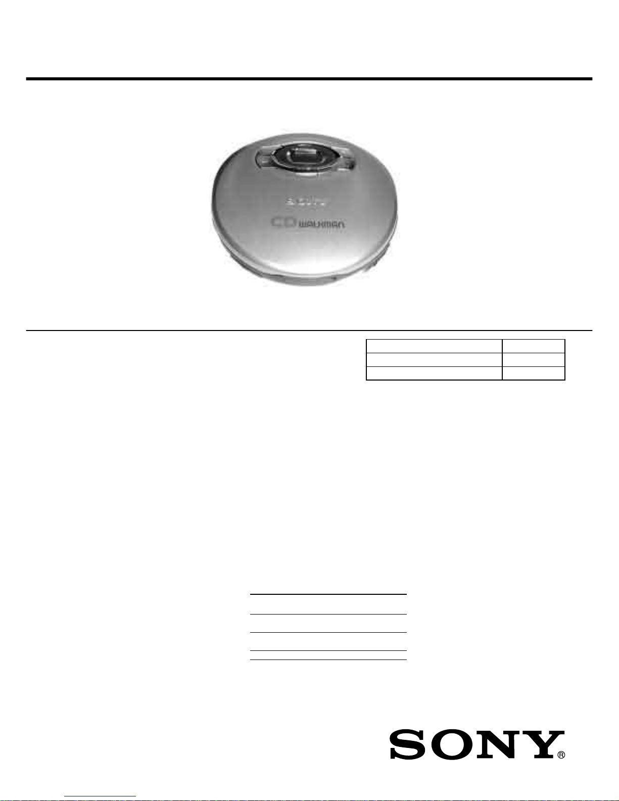
Photo : D-EJ611
Model Name Using Similar Mechanism NEW
CD Mechanism Type CDM-3223EBA
Optical Pick-up Type DAX-23E
System
Compact disc digital audio system
Laser diode properties
Material: GaAIAs
Wavelength : λ= 780 nm
Emission duration: Continuous
Laser output : Less than 44.6 µW
(This output is the value measured at a distance
of 200 mm from the objective lens surface on
the optical pick-up block with 7 mm aperture. )
D-A conversion
1-bit quartz time-axis control
Frequency response
20 - 20,000 Hz+1 dB (measured by EIAJ CP-
307)
-2
Output (at 4.5 V input level)
Line output (stereo minijack)
Output level 0.7 V rms at 47 kilohms
Recommended load impedance over 10
kilohms
Power requirements
For the area code of the model you purchased,
check the upper left side of the bar code on the
package.
• Two Sony NC-WMAA rechargeable
batteries: 2.4 V DC,
• Sony NH-WM2AA rechargeable batteries:
2.4 V DC,
• Two LR6 (size AA) batteries: 3 V DC
• AC power adaptor (DC IN 4.5 V jack):
US, Canadian, C&SA model: 120 V, 60 Hz
AEP, FR, G, EE, E13 model:
220 - 230 V, 50/60 Hz
UK model: 230 - 240 V, 50 Hz
EA model: 110 - 240 V, 50/60 Hz
AUS model: 240 V, 50 Hz
JE, E33 model: 100 - 240 V, 50/60 Hz
HK model: 220 V, 50/60 Hz
AR, CH model: 220 V, 50 Hz
• Sony DCC-E245 car battery cord for use on
car battery : 4.5V DC
Battery life* (approx. hours)
(When you use the CD player on a flat and
stable surface.)
Playing time varies depending on how the CD
player is used.
When using G-PROTECTION function
on off
Tow NC-WMAA 8 7
(charged for about 3 hours**)
NH-WM2AA 18 15
(charged for about 4 hours**)
Tow alkaline batteries LR6 32 28
* Measured value by the standard of EIAL
(Electronic Industries Association of Japan).
** Charging time varies depending on how the
rechargeable battery is used.
Operating temperature
5°C - 35°C (41°F - 95°F)
Dimensions (w/h/d) (excluding projecting
parts and controls)
Approx. 131 x 29 x 136 mm
( 51/4 x 13/16 x 53/8 in.)
Mass (excluding accessories)
Approx. 190 g (6.7 oz)
– Continued on page 2 –
9-927-632-12
2001G0200-1
© 2001.7
Sony Corporation
Personal Audio Company
Shinagawa Tec Service Manual Production Group

– 2 –
Specifications ............................................................................ 1
1. SERVICING NOTES................................................... 3
2. GENERAL
Locating the Controls......................................................... 4
3. DISASSEMBLY
3-1. Cabinet (Rear) Sub ASSY,
Cabinet (Front), Main Board....................................... 6
3-2. MD ASSY................................................................... 6
3-3. “Motor ASSY, Turn Table (Spindle) (M901)”............ 7
3-4. “Motor ASSY (Sled) (M902)”,
Optical Pick-up (DAX-23E) ...................................... 7
3-5. “Lid, Upper”, Switch Unit .......................................... 7
4. ELECTRICAL ADJUSTMENS ............................... 8
5. DIAGRAMS
5-1. Explanation of IC Terminals....................................... 9
5-2. Block Diagram...........................................................11
5-3. Printed Wiring Boards .............................................. 14
5-4. Schematic Diagram................................................... 17
6. EXPLODED VIEWS
6-1. Cabinet Section......................................................... 23
6-2. Optical pick-up Section (CDM-3223EBA) .............. 25
7. ELECTRICAL PAR TS LIST................................... 26
ATTENTION AU COMPOSANT AYANT RAPPORT
À LA SÉCURITÉ!
LES COMPOSANTS IDENTIFIÉS P AR UNE MARQUE 0 SUR LES
DIAGRAMMES SCHÉMATIQUES ET LA LISTE DES PIÈCES
SONT CRITIQUES POUR LA SÉCURITÉ DE FONCTIONNEMENT .
NE REMPLACER CES COMPOSANTS QUE PAR DES PIÈCES
SONY DONT LES NUMÉROS SONT DONNÉS DANS CE MANUEL
OU DANS LES SUPPLÉMENTS PUBLIÉS PAR SONY.
SAFETY-RELATED COMPONENT WARNING!!
COMPONENTS IDENTIFIED BY MARK 0 OR DOTTED LINE
WITH MARK 0 ON THE SCHEMATIC DIAGRAMS AND IN THE
PARTS LIST ARE CRITICAL TO SAFE OPERATION.
REPLACE THESE COMPONENTS WITH SONY PARTS WHOSE
PART NUMBERS APPEAR AS SHOWN IN THIS MANUAL OR IN
SUPPLEMENTS PUBLISHED BY SONY.
Flexible Circuit Board Repairing
• Keep the temperature of the soldering iron around 270°C during
repairing.
• Do not touch the soldering iron on the same conductor of the
circuit board (within 3 times).
• Be careful not to apply force on the conductor when soldering or
unsoldering.
Notes on chip component replacement
• Never reuse a disconnected chip component.
• Notice that the minus side of a tantalum capacitor may be damaged by heat.
TABLE OF CONTENTS
This Compact Disc player is
classified as a CLASS 1 LASER
product.
The CLASS 1 LASER
PRODUCT label is located on
the rear exterior.
CAUTION
Use of controls or adjustments or performance of procedures other
than those specified herein may result in hazardous radiation
exposure.
Laser component in this product is capable of emitting
radiation exceeding the limit for Class 1.
DANGER
Invisible laser radiation when open and interlock failed or defeated.
Avoid direct exposure to beam.
Supplied accessories
For the area code of the location in the which you purchased the CD
player, check the upper left side of the bar code on the package.
AC power adaptor (1) a –
Headphones /earphones with – a
remote control (1)
Headphones /earphones (1) a –
Rechargeable batteries (2) – a
Battery carrying case (1) – a
Strap (1) aa
For US customers
The AC power adaptor supplied is not intended to be serviced. Should AC
power adaptor cease to function in its intended manner, during the
warranty period, the adaptor should be returned to your nearest Sony
Service Center or Sony Authorized Repair Center for replacement, or
after warranty period, it should be discarded.
Design and specifications are subject to change without notice.
D-EJ615
D-EJ611
• Abbreviation
AUS : Australian
FR : French HK : Hong Kong
AR : Argentina JE : Tourist
G : German EA : Saudi Arabia
CH : Chinese EE : East European
C&SA :Central and South America
E13 : AC220-230V area model
E33 : AC100-240V area model
– 3 –
S801
The laser diode in the optical pick-up block may suffer electrostatic
breakdown because of the potential difference generated by the charged
electrostatic load, etc. on clothing and the human body. During repair,
pay attention to electrostatic breakdown and also use the procedure in
the printed matter which is included in the repair parts.
The flexible board is easily damaged and should be handled with care.
NOTES ON LASER DIODE EMISSION CHECK
The laser beam on this model is concentrated so as to be focused on the
disc reflective surface by the objective lens in the optical pick-up block.
Therefore, when checking the laser diode emission, observe from more
than 30cm away from the objective lens.
Before Replacing the Optical pick-up Block
Please be sure to check thoroughly the parameters as per the “Optical
pick-up Block Checking Procedure” (Part No. : 9-960-027-11) issued
separately before replacing the optical Pick-up block.
Note and specifications required to check are given below.
• FOK output : IC601 eg pin
When checking FOK, remove the lead wire to disc motor.
• RF signal P-to-P value : 0.4 to 0.5Vp-p
SECTION 1
SERVICING NOTES
Laser Diode Checking Methods
During normal operation of the equipment, emission of the laser diode
is prohibited unless the upper panel is closed while turning ON the S801
(push switch type).
The following two checking methods for the laser diode are operable.
Method :
Emission of the laser diode is visually checked.
1. Open the upper lid.
2. Push the S801 as shown in Fig. 1 .
3. Check the object lens for confirming normal emission of the laser
diode. If not emitting, there is a trouble in the automatic power
control circuit or the optical pick-up. During normal operation, the
laser diode is turned ON about 2.5 seconds for focus searching.
NOTES ON HANDLING THE OPTICAL PICK-UP BLOCK OR
BASE UNIT
Fig.1 Method to push S801
– 4 –
SECTION 2
GENERAL
LOCA TING THE CONTROLS
This section is extracted from
instruction manual.
– 5 –
– 6 –
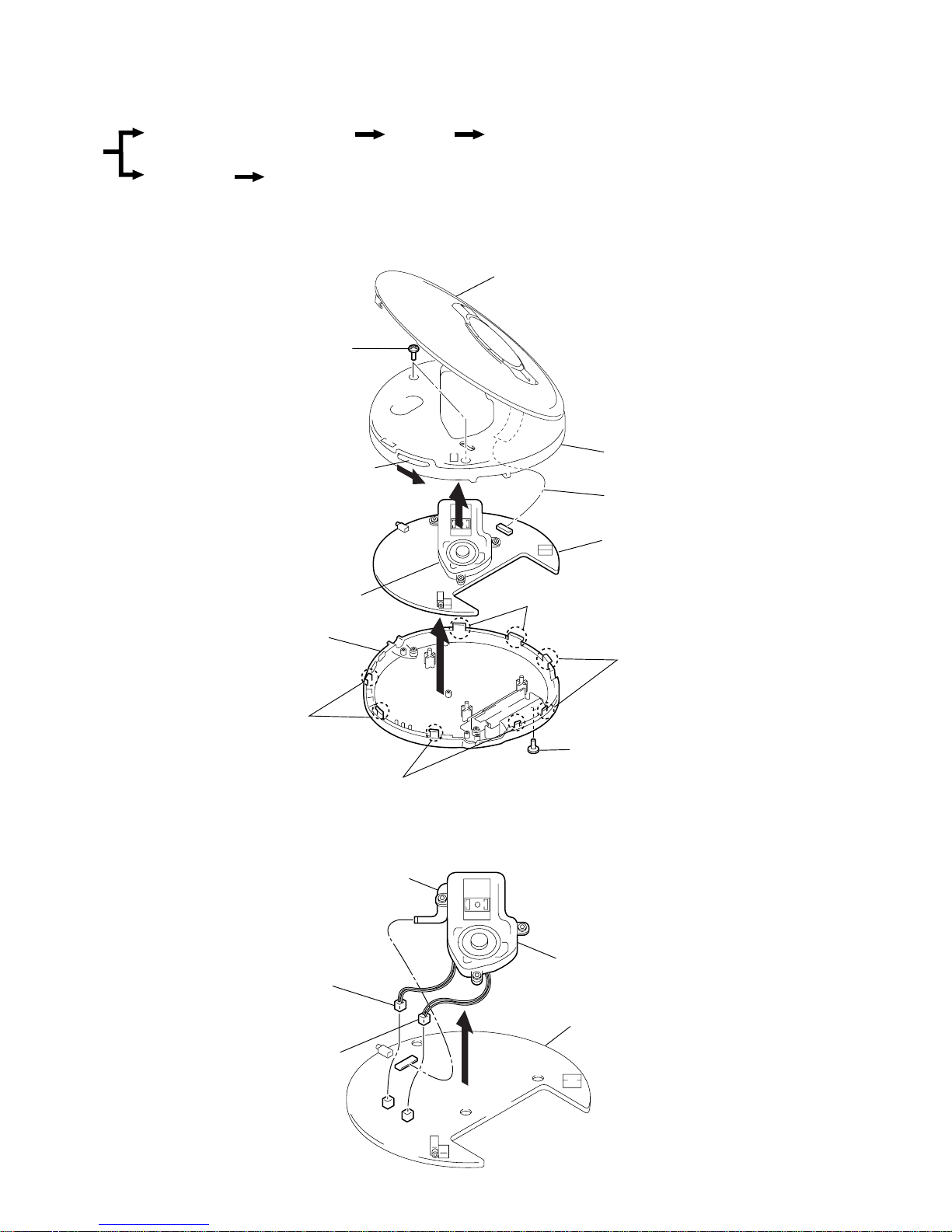
Cabinet (rear) sub ASSY, Main board MD ASSY
“Lid, Upper”, Switch unit
“Motor ASSY, Turn table (Spindle) (M901)”,
Optical pick-up (DAX-23E), “Motor ASSY (Sled) (M902)”
Cabinet (front)
Set
SECTION 3
DISASSEMBLY
Note : Follow the disassembly procedure in the numerical order given.
3-1. CABINET (REAR) SUB ASSY, CABINET (FRONT), MAIN BOARD
3-2. MD ASSY
z
The equipment can be removed using the following procedure.
4
1
CN502 (Green)
2
CN503 (White)
3
Optical pick-up flexible board
MD ASSY
Main board
3
Screws (B2)
5
7
1
Screw (B2)
2
OPEN
6
Flexible board (CN801)
Lid, Upper
Cabinet (Front)
Main board
MD ASSY
Cabinet (Rear) sub ASSY
4
Claws
4
Claws
4
Claws
4
Claws
– 7 –
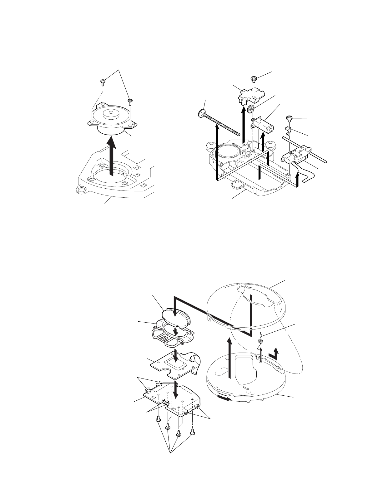
3-3. “MO TOR ASSY , TURN T ABLE
(SPINDLE) (M901)”
3-4. “MOTOR ASSY (SLED) (M902)”,
OPTICAL PICK-UP (DAX-23E)
3
5
6
2
1
Screw (B 1.7x5)
4
Screw
(P 1.4x3.5)
Screw ASSY, Feed
Chassis
Optical pick-up
(DAX-23E)
Bracket (Shaft)
Gear B
Cover, Gear
Motor ASSY (Sled) (M902)
2
Motor ASSY, Turn tabl
e
(Spindle) (M901)
1
Screws
(B1.7x5)
Chassis
3-5. “LID, UPPER”, SWITCH UNIT
2
4
3
1
OPEN
7
Cover ASSY, Lid
Lid, Upper
Cabinet (Front)
6
Claws
6
Claws
6
Claws
8
Switch unit
5
Screws
Spring (Full open)
q;
Window (LCD)
9
Button (Operate)
– 8 –
SECTION 4
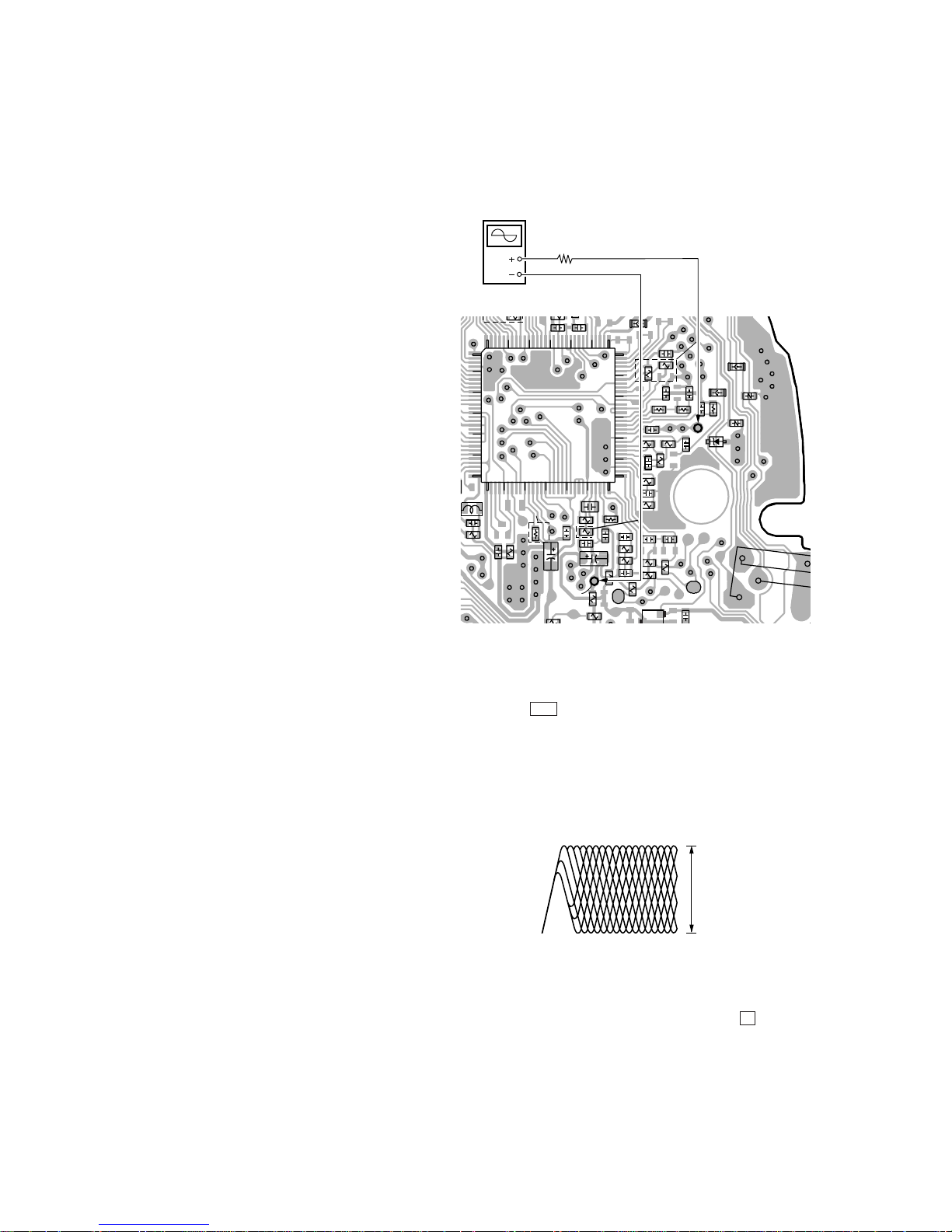
ELECTRICAL ADJUSTMENTS
The CD section adjustments are done automatically in this set.
Precautions for Check
1. Perform check in the order given.
2. Use YEDS-18 disc (Part No.: 3-702-101-01) unless otherwise
indicated.
3. Power supply voltage requirement : DC4.5 V in DC IN jack.
(J401)
VOLUME button : Minimum
AVLS switch : NORM
HOLD switch : OFF
Focus bias Check
Condition:
• Hold the set in horizontal state.
Connection:
Procedure:
1. Connect the oscilloscope to the test points TP629 (RF) and TP635
(GND) on the MAIN board.
2. Set a disc. (YEDS-18)
3. Press the u button.
4. Check the oscilloscope waveform is as shown below.
A good eye pattern means that the diamond shape (◊) in the center of the waveform can be clearly distinguished.
RF Signal reference Waveform (Eye Pattern)
To watch the eye pattern, set the oscilloscope to AC range and
increase the vertical sensitivity of the oscilloscope for easy
watch-ing.
5. Stop revolving of the disc motor by pressing the x button.
RF level
0.4 to 0.5 Vp-p
VOLT/DIV : 100 mV (With the 10 : 1 probe in use)
TIME/DIV : 500ns
S
TP608
C611
R604
C628
TP637
R633
TP639
R602
C618
1
TP619
C626
TP617
TP618
R606
R603
R608
C603
R611
R610
R609
TP635
(GND)
R605
C620
C607
C615
R
R
C609
C604
TP630
IC601
R613
C625
C623
C605
R615
R1
TP629
(RF)
C602
C613
R612
R639
FB602
FB101
C632
TP10
1
R643
US MODEL
FB301
L601
C638
R617
TP634
R614
TP631
C614
C622
R638
R630
0
4
C627
P601
R616
R619
C612
TAP602
TP632
TP633
R607
R641
C606
R632
TP301
TP305
D302
616
TP426
C631
TP413
7
8
9
VDR102
Q405
C635
VDR202
1
5
10
15
20
25
30
31 35
40
45 50 55 60
61
65
70
75
80
85
90
95100105110115120
91
EXCEPT
US MODEL
MODEL
EXCEPT
US MODEL
TP629 (RF)
TP635 (GND)
2 K
Ω
oscilloscope
(AC range)
[ MAIN BOARD] (Side B)

– 9 –
Pin No. Pin name I/O Description
1 VSS — Ground terminal.
2 IRRMCO — Not used (OPEN).
3 FOKI I Focus OK signal input from the digital servo processor (IC601). “L”: NG, “H”: OK
4 AGCPWM O AGC control pulse signal output terminal.
5 RESERVE — Not used (OPEN).
6 RESERVE — Not used (OPEN).
7 AMUTE O Analog audio muting ON/OFF control signal output terminal. “H”: muting ON
8 VCC2 ON O VCC2 voltage control signal output terminal.
9 XRST O Reset signal output to IC601. “L”: reset
10 SCK O Serial data transfer clock signal output to IC601.
11 MSDTI I Serial data input from the IC601.
12 MSDTO O Serial data output to IC601.
13 WAKE UP O WAKE-UP control signal output terminal (for system standby reset).
14 SEL I Plug-in detection signal input terminal of LINE OUT/OPTICAL OUT.
15 CHGMNT I Battery charge voltage detection input from the power control (IC401).
16 KEY2 I Volume key input terminal.
17 BATMNT I Battery voltage detection signal input terminal
18 KEY1 I Key input terminal.
19 RMKEY I Key input from the headphone with remote commander (A/D input).
20 DCINMNT I
DC input voltage detection input terminal (A/D input) and DC input jack use/no use
detection input terminal.
21 OPEN I
CD door open/close detection switch (S801) input terminal.
The stop status is reset with the falling edge of input signal.
22 VREFL I Reference voltage input terminal (0V) for A/D converter.
23 VREFH I Reference voltage input terminal (+2V) for A/D converter.
24 VDD — Power supply terminal (+2V).
25 SCOR I Sub-code sync (S0+S1) detection signal input from the IC601.
26 GRSCOR I GRSCOR signal input from the IC601.
27 FG I FG pulse signal input.
28 BEEP O Beep sound output to the headphone amplifier (IC302).
29 RESERVE — Not used ( Fixed at “H”).
30 RMSCK O Communication clock output to the communication format converter (IC802).
31 RMDATI I
Communication data bus input of headphone with remote commander from the communi-
cation format converter (IC802).
32 RMDATO O
Communication data bus output of headphone with remote commander to the communi-
cation format converter (IC802).
33 RMRW O
Read/write control signal output of headphone with remote commander to the communi-
cation format converter (IC802). “L”: read mode, “H”: write mode
34 RMLAT O
Serial data latch pulse signal output of headphone with remote commander to the commu-
nication format converter (IC802).
35 WFCKI I WFCK signal input from the IC601.
36 COMPRESSION I G PROTECTION switch input.
37 SLVCD I Not used (Fixed at “H”).
38 AVLS I
AVLS (Automatic Volume Limiter System) switch (S803) input terminal.
“L”: normal mode, “H”: limit mode
39 HOLD I HOLD switch (S803) input terminal. “L”: hold ON, “H”: hold OFF
40 BATT DET I External battery detection signal input terminal.
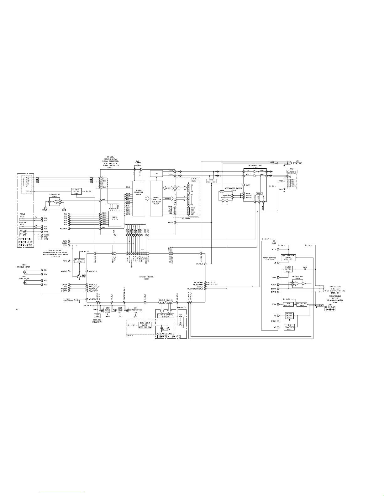
SECTION 5
DIAGRAMS
5-1. EXPLANATION OF IC TERMINALS
IC801 (SYSTEM CONTROLLER) TMP88CM22F-MIR1-1

– 10 –
Pin No. Pin name I/O Description
41 X3037 O Mode select terminal for IC601.
42 XHGOM O Optical pick-up power ON/OFF control signal output terminal. “L”: ON
43 XLAT O Serial data latch pulse signal output to IC601.
44 XSOE O Serial data output enable signal output terminal.
45 HP ATTENUATION O Headphone attenuater ON/OFF signal output.
46 XPOWLT O Latch signal output to the power control (IC401).
47 RESERVE O Not used (Fixed at “H”).
48 XAPC OFF O APC mute signal output terminal. “L”: mute
49 SEG15 — Not used (open).
50 to 64 SEG14 to SEG0 O Segment drive signal output to the liquid crystal display.
65 to 68 COM3 to COM0 O Common drive signal output to the liquid crystal display.
69 to 71 V3 to V1 O Bias signal output to the liquid crystal display driver.
72, 73 C1, C0 O Capacitor connected terminal for the liquid crystal display driver voltage-up.
74 STOP O VCD control stop signal output terminal. Not used (Fixed at “L”).
75 TEST I Test terminal for IC (Fixed at “L”).
76 BBSW O ON/OFF control signal output to the headphone amplifier (IC302).
77 XLED O LCD back light control signal output to the liquid crystal display. (EJ616CK)
System reset signal input from the power control (IC401). “L”: reset
78 RESET I For several hundreds msec. after the power supply rises, “L” is input, then it changes to
“H”
79 XIN I System clock input terminal.
80 XOUT — Not used (OPEN).
– 11 – – 13 –– 12 –
5-2. BLOCK DIAGRAM
• Signal path.
J : CD
D-E660/EJ610/EJ611/EJ613/EJ615/EJ616CK
– 14 – – 16 –– 15 –
D-E660/EJ610/EJ611/EJ613/EJ615/EJ616CK
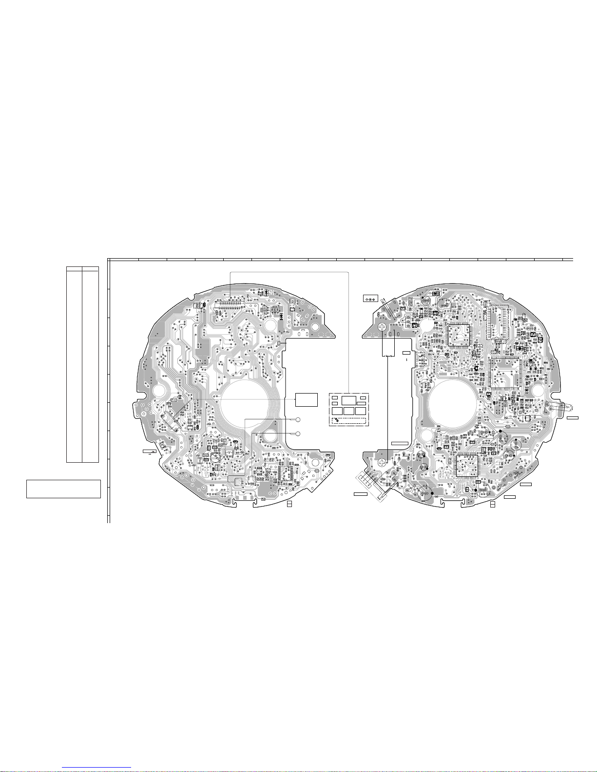
5-3. PRINTED WIRING BOARDS
Note:
• X : parts extracted from the component side.
• b : Pattern from the side which enables seeing.
(The other layers' patterns are not indicated.)
Caution:
Pattern face side: Parts on the pattern face side seen from the
(Side B) pattern face are indicated.
Parts face side: Parts on the parts face side seen from the
(Side A) parts face are indicated.
• Abbreviation
CND :Canadian AUS :Australian
FR : French HK :Hong Kong
AR : Argentina JE :Tourist
G :German EA : Saudi Arabia
CH : Chinese EE :East European
C&SA : Central and South America
D301 H-10
D302 E-16
D401 B-7
D403 B-10
D404 B-6
D405 G-5
D406 G-12
D409 C-11
D461 F-4
D601 D-13
D602 B-4
D603 D-13
D804 B-4
D805 B-4
D901 B-12
IC302 H-7
IC310 H-6
IC401 H-13
IC402 F-13
IC404 F-12
IC601 D-14
IC602 C-14
IC801 C-13
Q301 C-15
Q302 C-16
Q401 C-11
Q402 B-6
Q403 B-6
Q404 B-7
Q405 F-15
Q406 G-13
Q407 F-14
Q408 G-5
Q411 C-11
Q412 B-11
Q500 E-3
Q900 B-12
Q902 B-6
Q904 D-13
VDR101 H-11
VDR102 D-16
VDR201 H-11
VDR202 E-16
VDR301 H-10
VDR303 H-11
Ref. No. Location
z
Semiconductor
Location
2
3 4 5 6 7
8
9 10 11 12 13 14
15
16
A
1
B
C
D
E
F
G
H
I
1
ECB
1
5
10
12
13
15
20
24
1
5
10
1314
15
20
25
26
D
S
G
1
60
5
55
10
50
15
45
20
21
80
25753070356540
61
41
1
60
5
55
10
1
34
5
15
50
45
20
21
80
25753070356540
61
41
S802
AVLS
NORM
LIMIT
SWITCH UNIT
LIQUID
CRYSTAL
DISPLAY
PLAY
MODE
REPEAT/
ENTER
SOUND
(LCD BACK-LIGHT)
u
x /CHG
>
.
EJ616CK
OPTICAL PICK-UP
BLOCK
DAX-23E
M
M
M901
SPINDLE
MOTOR
M902
SLED
MOTOR
E
C
B
DRY BATTERY
SIZE "AA"
(IEC DESIGNATION LR6)
2PCS, 3V
RECHAGEABLE
BATTERY
NC-WMAA/NH-WM2AA
2.4V
S801
(OPEN/CLOSE)
-1
-2
-1
-2
02
R206
R807
TP608
TP800
TP403
TP428
IC801
TP421
EJ616CK
EJ616CK
TP420
IC401
IC602
C611
C417
R423
R104
R202
R103
R604
C203
R424
C424
C636
C103
R821
TP824
C628
TP641
TP637
TP412
R633
TP639
R2
R602
TP815
TP419
TP434
TP402
C618
TP409
R209
C407
R422
R432
C402
R427
C621
TP429
TP803
TP619
C626
TP617
TP618
C423
R606
R603
R608
C603
R623
R611
R610
TP822
TP417
C413
R102
R609
TP635
(GND)
R605
C620
TP804
C607
C615
R621
R654
R803
R820
R824
C609
C604
Q412
TP630
IC601
C442
R809
R440
L412
L406
R846
Q904
R801
R811
R613
C639
R109
EXCEPT
US MODEL
EXCEPT
US MODEL
R421
C625
D301
R451
L410
Q900
R409
L408
C623
FB603
FB201
R802
TP649
C403
C811
C605
R615
R1
TP629
(RF)
C602
C613
R612
R805
Q411
C426
R823
TP844
R639
TP507
TP508
TP837
TP506
TP501
TP502
TP503
TP504
C101
TP827
TP842
TP832
TP829
TP830
TP831
C801
TP418
TP814
R457
C807
R624
R826
R843
R830
R812
R625
R813
Q302
EXCEPT US
MODEL
C201
FB602
FB311
FB101
C632
TP650
R106
R205
R105
R101
X601
C404
TP201
TP101
R3
R322
R439
TP840
TP424
TP416
R643
US MODEL
R904
R449
R447
D409
FB211
FB312
FB301
C312
R829
L601
TP431
TP435
R401
R201
TP311
TP312
TP313
TP314
TP111
TP211
C422
TP315
TP102
TP816
C425
TP839
TP838
R645
TP826
R842
R415
TP843
D406
TP836
R835
R814
R901
TP809
C810
C401
R416
C803
R417
C414
R418
R808
TP430
C800
R628
C408
TP849
R443
C416
C415
R420
R437
TP845
L402
C809
C630
C400
C202
TP203
IC404
C638
C812
TP423
TP841
R617
TP834
TP634
R614
TAP403
TP609
C802
TP828
TAP401
TP802
R646
TP631
C430
TP411
TP823
R452
R903
R430
C102
R453
R902
R834
Q406
TP833
TP610
TP825
C614
C808
C622
R638
TP817
R630
R627
TP615
R629
TP612
R810
D601
TP603
TP604
TP606
TP611
C804
R644
R454
R455
-1
-2
-2
-1
R442
C627
TAP601
R616
R619
R408
C612
TAP602
TP632
TP633
BT401
BT402
TP410
TP422
R607
R402
R446
R641
TP835
R204
TP404
C451
TP405
TP303
C606
L409
Q407
TAP402
R632
TP847
TP805
TP846
TP820
C438
TP850
TP812
TP901
TP902
TP819
TP301
TP848
TP305
D302
TP437
TP509
TP439
TP447
TP404
C453
R448
C619
C616
TP406
Q301
R626
TP616
TP425
TP426
C631
R640
TP413
R647
R648
R649
VDR101
VDR201
VDR303
VDR301
VDR102
Q405
S802
R419
R456
C635
D901
R318
R653
C629
R319
R320
VDR202
D603
R818
C805
C806
C814
R426
TP806
TP818
TP810
R203
BT400
C634
C418
C353
C352
C354
C406
S805
C410
S804
C409
S806
C431
C900
Q401
TP627
TP613
IC302
C462
R254
R313
C104
TAP801 (TEST)
NORMAL MODE:OPEN
TEST MODE:SHORT
R154
R827
R435
TP407
Q902
C432
R207
R429
D404
C502
C433
R461
L407
L404
TP440
C303
TP621
TP202
1
4
5
8
C411
TP103
TP446
C624
CN501
C461
R253
CN503
(WHT)
C254
R107
R436
L405
Q500
R467
D461
R634
C419
R410
C427
TP461
C204
C435
TP851
Q408
C841
C300
L311
IC310
R353
R841
TAP802
(OPEN)
R316
R434
D405
R403
C351
R471
TP636
R431
C421
C205
R208
C420
TP414
C405
C105
R315
R111
FB111
C154
CN801
R450
C302
C313
Q403
C500
R110
R636
R642
L411
Q404
TP401
TP104
C501
TP622
L401
CN502
(GRN)
TP628
TP625
TP626
TP623
TP624
TP505
TP415
TP807
R210
TP438
TP444
TP441
TP442
TP445
TP906
TP443
TP432
TP302
TP408
C106
R314
C304
C301
R211
R153
TP808
IC402
C412
D401
TP427
TP801
D804
D805
Q402
R465
R463
R462
TP433
L403
TP448
TP449
TP436
TP306
R321
S803
D602
TP813
TP620
S803
HOLD
OFF ON
1
5
10
15
20
25
30
31 354045 50 55 60
61
65
70
75
80
85
90
95100105110115120
91
[MAIN BOARD] (SIDE A)
13
45
12
(12)
1-675-135-
12
(12)
1-675-135-
[MAIN BOARD] (SIDE B)
DC IN 4.5V
J401
S804
G PROTECTION
OFFTON
J302
i/REMOTE
S806
VOLUME–
S805
VOLUME+
J301
LINE OUT
EXCEPT
US MODEL
US MODEL
US
MODEL
EXCEPT
US MODEL
EXCEPT
US MODEL
EXCEPT
US MODEL
EXCEPT
US MODEL
EXCEPT
US MODEL
US MODEL
D403
US MODEL
EXCEPT
US MODEL
– 17 – – 18 – – 20 –– 19 –
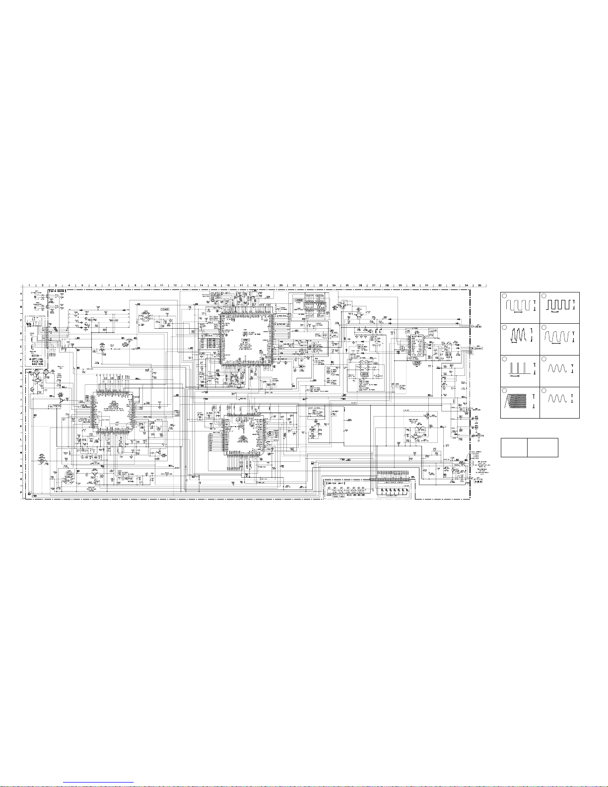
5-4. SCHEMATIC DIAGRAM
D-E660/EJ610/EJ611/EJ613/EJ615/EJ616CK
Note:
• All capacitors are in µF unless otherwise noted. pF: µµF
50 WV or less are not indicated except for electrolytics
and tantalums.
• All resistors are in Ω and 1/
4
W or less unless otherwise
specified.
Note: Note:
The components identi- Les composants identifiés
fied by mark 0 or dotted par une marque 0 sont criline with mark 0 are cri- tiques pour la sécurité.
tical for safety. Ne les remplacer que par
Replace only with part une piéce portant le
number specified. numéro spécifié.
• U : B+ Line.
• Power voltage is dc 4.5V and fed with regulated dc power
supply from external power voltage jack (J401).
• Voltages and waveforms are dc with respect to ground
under no-signal conditions.
no mark : PLAY
∗
: Impossible to measure
• Voltages are taken with a VOM (Input impedance 10 MΩ).
Voltage variations may be noted due to normal production tolerances.
• Waveforms are taken with a oscilloscope.
Voltage variations may be noted due to normal production tolerances.
• Circled numbers refer to waveforms.
• Signal path.
J : CD
• Abbreviation
CND : Canadian
AUS :Australian
FR : French
HK : Hong Kong
AR : Argentina
JE :Tourist
G : German
EA : Saudi Arabia
CH : Chinese
EE : East European
C&SA: Central and South America
z
Refer to page 21 – 22 for IC Block Diagrams.
r
Waveforms
1
IC601 wg
CLOCK
5
2 6
3 7
4 8
VOLT/DIV : 0.5 V AC
TIME/DIV : 0.5 µsec
IC601 ih
LRCK
IC601 e;
R4M
IC601 o;
BCK
IC601 rd
MDP
IC601 of
XTAO
IC601 ua
RFAC
IC801 ul
XIN
VOLT/DIV : 0.5 V AC
TIME/DIV : 0.1 µsec
PLAY MODE
VOLT/DIV :0.5 V AC
TIME/DIV : 2 µsec
VOLT/DIV : 0.1 V AC
TIME/DIV : 0.5 msec
VOLT/DIV : 0.5 V AC
TIME/DIV : 5 µsec
VOLT/DIV : 0.5 V AC
TIME/DIV : 0.1 µsec
VOLT/DIV : 0.2 V AC
TIME/DIV : 20 nsec
VOLT/DIV : 0.5 V AC
TIME/DIV : 0.1 µsec
2.1 Vp-p
1.9
µ
sec
1.76 Vp-
p
239 nsec
2.1 Vp-p
3.8
µ
sec
400 – 500
mVp-p
2 Vp-p
22.9
µ
sec
2.1 Vp-p
479 nsec
0.9 Vp-p
16.9MHz
2.6 Vp-
p
4MHz

– 23 – – 24 –– 21 – – 22 –
z
IC Block Diagrams
IC302 TA2120FN (EL)
+
–
+
–
+
–
23
20 19 18
17
16
15
14
13
2
3
4 5
6
7
8
9
101112
1
24
BIAS
BEEP
PWSWMT
SW
ALC
DET
ATT
SW
PWC
SW
OUT B
OUT A
BEEP
BST
PW
B
PW
C
BSTNFADD
OUT
RF IN OCLSW ROUT VREF LOUT PWR
GND
MIX
OUT
ALCINALC
DET
ATT
SWLINRINGNDTC
MUTE MUTESWPWR
SWBIAS
BIASIN BBSWBST
OUT
VCC
ADD
A
ADD
B
21
22
PW
A
ALC ALC
IC601 CXD3037R
ERROR
CORRECTOR
32K
RAM
EFM
DEMODULATOR
SUB CODE
PROCESSOR
SERVO
AUTO
SEQUENCER
D/A
INTERFACE
VIBRATION
MEMORY
CONTROLLER
+
COMPRESSION
EXPANDER
DAC
SELECTOR
DIGITAL
OUT
ASYMMETRY
CORRECTOR
DIGITAL
PLL
DIGITAL
CLV
CPU
INTERFACE
OP AMP
ANALOG SWITCH
SERVO BLOCK
SIGNAL
PROCESSOR
BLOCK
MEMORY CONTROLLER,
BUS BOOST BLOCK
A/D
CONVERTER
SERVO
INTERFACE
SERVO DSP
FOCUS SERVO
SLED SERVO
TRACKING
SERVO
CLOCK
GENERATOR
LPF
LPF
MIRR
DFCT
FOK
PWM GENERATOR
FOCUS PWM
GENERATOR
SLED PWM
GENERATOR
TRACKING PWM
GENERATOR
90
89
88
87
86
85
84
83
82
81
80
79
78
77
76
75
74
73
72
71
70
69
68
67
66
65
64
63
62
61
1
2
3
4
5
6
7
8
9
10
11
12
13
14
15
16
17
18
19
20
21
22
23
24
25
26
27
28
29
30
31 32 33 34 35 36 37 38 39 40 41 42 43 44 45 46 47 48 49 50 51 52 53 54 55 56 57 58 59 60
XOE
A0 – A11
SYSM
AMUTE
HPL
HPM
HPR
PCMDI
LRCKI
BCKI
AOUT1
AIN1
LOUT1
LOUT2
AIN2
AOUT2
A9
A8
A7
DVSS
RFAC
XTAO
XTAI
XTSL
VCTL
VPCO
WFCK
GFS
XUGF
MDS
C2PO
WDCK
BIAS
ASYI
ASYO
FILO
FILI
PCO
PWMI
LOCK
MDP
SDTI
SCSY
SCOR
SBSO
EXCK
SDTO
XLAT
CLOK
SENS
XSOE
R4M
IGEN
VDD0
COUT
MIRR
DFCT
FOK
PWMI/HPVSS
LOCK/HPL
HPR
HPM
HPL/HPVDD
VDD1
C176
MDP
MDS
SSTP
SFDR
SRDR
TFDR
TRDR
FFDR
FRDR
FRDR
FFDR
TRDR
TFDR
SRDR
SFDR
SCLK
ATSK
SSTP
COUT
FOK
DFCT
MIRR
VSS1
TEST
TES1
AVDD0
IGEN
AVSS0
RFDC
E
F
120119 118 117 116 115 114 113 112 111 110 109 108 107 106 105 104 103 102 101 100 99 98 97 96 95 94 93 92 91
XOE
XCASD2D3D0D1
XWE
XRAS
A11
A10
DVDDA0A1A2A3
AVDD2
LOUT2
AIN2
AOUT2
AVSS2
AVSS1
AOUT1
AIN1
LOUT1
AVDD1
XVSS
XTAO
XTAI
XVDD
BCKI
XOE
XCAS
D2D3D0
D1
XWE
XRAS
A11
A10
DVDD
A0A1A2
A3
AVDD2
LOUT2
AIN2
AOUT2
AVSS2
AVSS1
AOUT1
AIN1
LOUT1
AVDD1
XVSS
XTAO
XTAI
XVDD
BCKI
VDD0
COUT
MIRR
DFCT
FOK
PWMI
LOCK
HPR
HPM
HPL
VDD1
MDP
MDS
SSTP
SFDR
SRDR
TFDR
TRDR
FFDR
FRDR
VSS1
A VDD
A GND
D VDD
AVDD0
IGEN
AVSS0
RFDC
E
F
RFDC
E
F
B
A
VC
CLTV
XPCK
A6
A5/PWMI
XWRE
XRDE
XEMP
XWIH
XQOK
AMUTE
SDTI
XQCK
SCSY
SCOR
VSS0
SBSO
EXCK
XRST
SYSM
SDTO
XLAT
CLOK
SENS
SCLK
XSOE
ATSK
R4M
A9
A8
A7
DVSS
A6
A5
A4
XWRE
XRDE
XEMP
XWIH
XQOK
AMUTE
SDTI
SCSY
SCOR
VSS0
D GND
SBSO
EXCK
SYSM
SDTO
XLAT
CLOK
SENS
SCLK
XSOE
ATSK
R4M
BCK
PCMDI
PCMD
LRCKI
LRCK
DOUT
VDD2
WFCK
C2PO
GFS
XPCK
XUGF
WDCK
VSS2
XTSL
AVDD3
ASYO
ASYI
BIAS
RFAC
AVSS3
CLTV
PCO
FILI
FILO
VCTL
VPCO
VC
A
B
BCK
PCMDI
PCMD
LRCKI
LRCK
DOUT
VDD2
WFCK
C2PO
GFS
XPCK
XUGF
WDCK
VSS2
XTSL
AVDD3
ASYO
ASYI
BIAS
RFAC
AVSS3
CLTV
PCO
FILI
FILO
VCTL
VPCO
VC
A
B
XCAS
D0 – D4
XWE
BCK
PCMD
LRCK
DOUT
XWRE
XRAS
XRDE
XQOK
XWIH
XEMP
A4
SECTION 6
EXPLODED VIEWS
NOTE :
• -XX, -X mean standardized parts, so they
may have some difference from the original
one.
• Color indication of Appearance Parts
Example :
KNOB, BALANCE (WHITE) ••• (RED)
↑↑
Parts color Cabinet's color
• Items marked “ * ”are not stocked since they
are seldom required for routine service. Some
delay should be anticipated when ordering
these items.
• The mechanical parts with no reference
number in the exploded views are not
supplied.
• Hardware (# mark) list and accessories and
packing materials are given in the last of this
parts list.
6-1. CABINET SECTION
Les composants identifiés par une
marque 0 sont critiques pour la sécurité.
Ne les remplacer que par une pièce
portant le numéro spécifié.
The components identified by mark 0
or dotted line with mark 0 are critical
for safety.
Replace only with part number specified.
• Abbreviation
CND : Canadian AUS : Australian
FR : French HK :Hong Kong
AR : Argentina JE :Tourist
G :German EA :Saudi Arabia
CH : Chinese EE : East European
C&SA: Central and South America
E13 : AC220-230V area model
E33 : AC100-240V area model
1
2
3
4
5
6
7
8
9
10
11
11
12
13
14
15
16
17
18
18
19
20
21
22
23
CDM-3223EB
A
24
not
supplied
Ref. No. Part No. Description Remark Ref. No. Part No. Description Remark
1 A-3328-742-A CABINET (REAR) SUB ASSY
2 4-966-278-01 FOOT,RUBBER
3 4-223-586-01 TERMINAL, BATTERY LINK
4 4-993-131-01 KNOB(HOLD)
4 4-993-131-21 KNOB(HOLD) (FOR BLUE)(E660,EJ661,EJ613,
EJ615)
5 A-3323-399-A MAIN BOARD, COMPLETE (EXCEPT FR/
EJ616CK)
5 A-3323-400-A MAIN BOARD, COMPLETE (FR)
5 A-3323-401-A MAIN BOARD, COMPLETE (EJ616CK)
5 A-3323-464-A MAIN BOARD, COMPLETE
(EJ611:US/EJ615:US)
5 A-3323-465-A MAIN BOARD, COMPLETE (EJ616CK:US)
6 4-223-583-01 SPRING (OPEN)
7 4-222-794-01 CLAW,LOCK
8 4-222-793-11 KNOB(OPEN)
8 4-222-793-21 KNOB(OPEN) (FOR BLUE)
(E660,EJ661,EJ613,EJ615)
9 4-223-607-01 BUTTON (VOLUME)
9 4-223-607-11 BUTTON (VOLUME) (FOR BLUE)
(E660,EJ661,EJ613,EJ615)
10 4-222-792-01 LEVER, DETECTOR
11 3-375-114-31 SCREW
12 X-3378-320-1 COVER ASSY, LID (EJ611:AUS,E13)
12 X-3378-321-1 COVER ASSY, LID (EJ611:AUS,E13)
12 X-4952-143-1 COVER ASSY, LID (SILVER)
12 X-4952-401-1 COVER ASSY, LID (BLUE)
(E660,EJ611:EXCEPT C&SA,EE,EA,AR,EJ613,
EJ615:EXCEPT CND,FR,EE)
12 X-4952-403-1 COVER ASSY, LID (BLACK) (EJ611:AEP,UK,FR,
G,AUS,E13/EJ615:AEP,UK)
12 X-4952-404-1 COVER ASSY, LID (YELLOW) (EJ611:AEP,G,
AUS E13,EJ615:AEP,FR)
13 1-418-612-11 SWITCH UNIT (EJ616CK)
13 1-418-638-11 SWITCH UNIT (EXCEPT EJ616CK)
14 4-223-612-01 BUTTON (OPERATE)
15 4-223-611-01 COVER, DECORATION
16 4-223-610-01 WINDOW (LCD)
17 3-042-673-11 LID,UPPER (SILVER)(EJ616CK:US,CND,AUS,
E13,E33,C&SA,EA)
17 3-042-673-01 LID,UPPER (SILVER) (EJ610)
17 3-042-673-21 LID,UPPER (SILVER) (EJ616CK:AEP,EE,G)
17 4-223-605-01 LID,UPPER (SILVER) (EJ615:US,CND,AUS,
E13,E33,HK,CH)
17 4-223-605-11 LID,UPPER (BLUE) (EJ615:US,CND,AUS,
E13,E33,C&SA,HK,CH)
17 4-223-605-21 LID,UPPER (BLACK) (EJ615:AEP,UK)
17 4-223-605-31 LID,UPPER (YELLOW) (EJ615:AEP,FR)
17 4-223-605-41 LID,UPPER (BLACK) (EJ615:AEP,UK)
17 4-223-605-51 LID,UPPER (YELLOW) (EJ615:AEP)
17 4-223-605-61 LID,UPPER (SILVER) (E660)
17 4-223-605-71 LID,UPPER (BLUE) (E660)
17 4-223-605-81 LID,UPPER (SILVER) (EJ613)
17 4-223-605-91 LID,UPPER (SILVER) (EJ613)
17 4-225-281-01 LID,UPPER (SILVER) (EJ611:EXCEPT AEP,G,
UK,FR,EE)
17 4-225-281-11 LID,UPPER (BLUE) (EJ611:EXCEPT AEP,G,UK,
FR,EE)
17 4-225-281-21 LID,UPPER (BLACK) (EJ611:EXCEPT
AEP,G,UK,FR,EE)
17 4-225-281-31 LID,UPPER (YELLOW) (EJ611:EXCEPT
AEP,G,UK,FR,EE)
17 4-225-281-41 LID, UPPER (EJ611:EXCEPT AEP,G,UK,FR,EE)
17 4-225-281-51 LID, UPPER (EJ611:EXCEPT AEP,G,UK,FR,EE)
17 4-225-281-61 LID, UPPER (SILVER) (EJ611:AEP,FR,G,EE,UK)
17 4-225-281-71 LID, UPPER (BLUE)(EJ611:AEP,FR,G,UK)
17 4-225-281-81 LID, UPPER (BLACK)(EJ611:AEP,FR,G,UK)
17 4-225-281-91 LID, UPPER (YELLOW) (EJ611:AEP,G)
18 4-908-792-51 SCREW (B2)
19 4-223-587-01 SPRING (FULL OPEN)
20 4-223-603-01 CABINET (FRONT) (DARK GRAY)
20 4-223-603-11 CABINET (FRONT) (BLUE) (E660,EJ611:
EXCEPT C&SA,EE,EA,AR,EJ613,EJ615:
EXCEPT US,CND,C&SA,FR,EE)
21 4-223-584-01 TERMINAL (-), BATTERY
22 4-223-606-01 LID,BATTERY (SILVER,BLACK)
22 4-223-606-11 LID, BATTERY (BLUE) (E660,EJ611:
EXCEPT C&SA,EE,EA,AR,EJ613,EJ615:
EXCEPT US,CND,C&SA,FR,EE)
22 4-223-606-21 LID, BATTERY (YELLOW)
(EJ611:AEP,G,AUS,E13,EJ615:AEP,FR)
23 4-223-592-01 PSA(LCD WINDOW)
24 4-223-609-01 KNOB(JOGGABLE) (SILVER/BLACK)
24 4-223-609-11 KNOB (JOGGABLE) (BLUE) (E660,EJ611:
EXCEPT C&SA,EE,EA,AR,EJ613,EJ615:
EXCEPT US,CND,C&SA,FR,EE)
24 4-223-609-21 KNOB (JOGGABLE) (YELLOW)
(EJ611:AEP,G,AUS,E13,EJ615:AEP,FR)
Ver 1.4 2000.10
 Loading...