


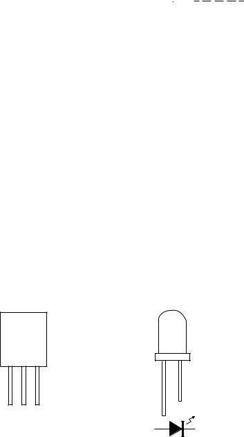
CD-BP2000W/210W/2000A/BK2000W/210W
SERVICE MANUAL
No. S4032CDBP2000
CD-BP2000W
CD-BP210W
|
CD-BP2000W/BP210W mini component system consisting of |
Illustration: CD-BP2000W |
CD-BP2000W/BP210W (main unit) and CP-BP2000/210 |
(speaker system). |
Illustration: CD-BK210W
•In the interests of user-safety the set should be restored to its original condition and only parts identical to those specified be used.
CD-BK2000W
CD-BK210W
CD-BK2000W/BK210W mini component system consisting of CD-BK2000W/BK210W (main unit) and CP-BP2000/210 (speaker system).
CD-BP2000A
CD-BP2000W mini component system consisting of CD-BP2000W (main unit) and CP-BP2000A (speaker system).
|
CONTENTS |
|
|
|
Page |
SAFETY PRECAUTION FOR SERVICE MANUAL ........................................................................................... |
................ 2 |
|
VOLTAGE SELECTION .............................................................................................................. |
....................................... 2 |
|
SPECIFICATIONS ................................................................................................................. |
............................................ 3 |
|
NAMES OF PARTS ................................................................................................................. |
.......................................... 4 |
|
OPERATION MANUAL .............................................................................................................. |
....................................... 7 |
|
DISASSEMBLY .................................................................................................................... |
.............................................. 9 |
|
REMOVING AND REINSTALLING THE MAIN PARTS ....................................................................................... |
............ 13 |
|
ADJUSTMENT ..................................................................................................................... |
............................................ 14 |
|
NOTES ON SCHEMATIC DIAGRAM ..................................................................................................... |
......................... 16 |
|
WAVEFORMS OF CD CIRCUIT ........................................................................................................ |
.............................. 17 |
|
BLOCK DIAGRAM .................................................................................................................. |
......................................... 18 |
|
SCHEMATIC DIAGRAM / WIRING SIDE OF P.W.BOARD .............................................................................................. |
22 |
|
VOLTAGE ........................................................................................................................ |
................................................ 42 |
|
TROUBLESHOOTING ................................................................................................................ |
..................................... 43 |
|
FUNCTION TABLE OF IC........................................................................................................... |
..................................... 47 |
|
FL DISPLAY ...................................................................................................................................................................... |
55 |
|
REPLACEMENT PARTS LIST/EXPLODED VIEW
DIFFERENCE BETWEEN CD-BP2000W/2000A/210W AND CD-BK2000W/210W
|
|
CD-BP2000W/2000A/210W |
CD-BK2000W/210W |
|
|
|
|
|
|
|
Karaoke |
None |
Used |
|
|
|
|
|
|
|
|
|
|
|
|
|
|
|
|
This document has been published to be used
SHARP CORPORATION– 1 – |
for after sales service only. |
|
|
|
The contents are subject to change without notice. |
CD-BP2000W/210W/2000A/BK2000W/210W
SAFETY PRECAUTION FOR SERVICE MANUAL
WARNINGS
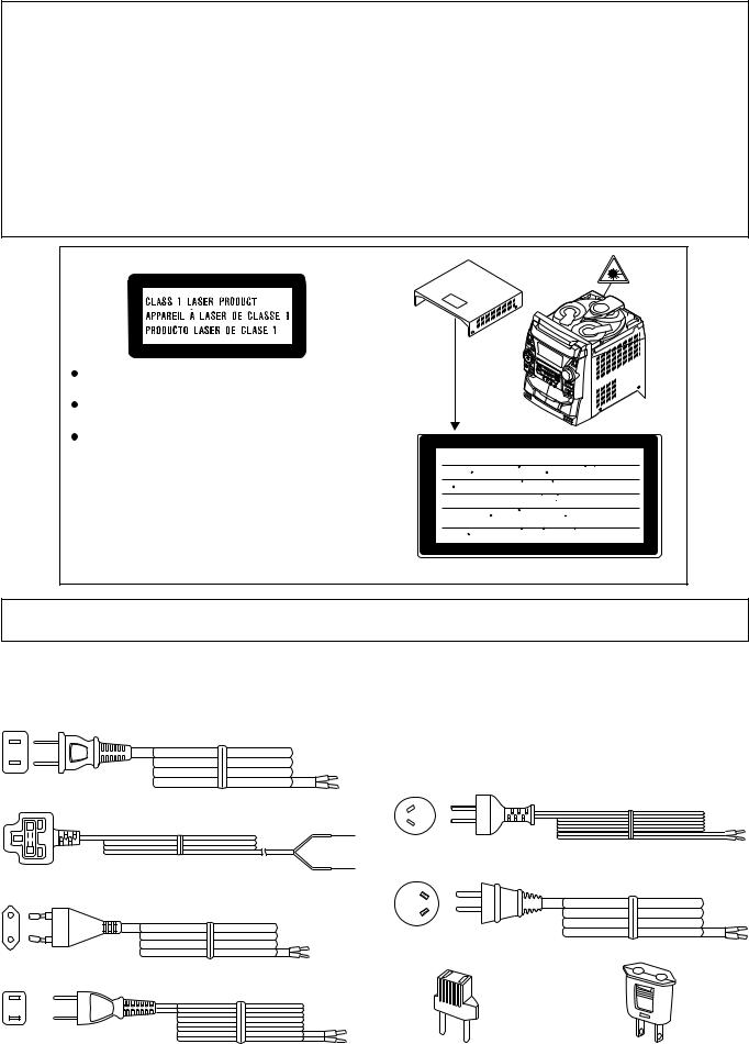
THE AEL (ACCESSIBLE EMISSION LEVEL) OF THE LASER POWER OUTPUT IS LESS THAN CLASS 1 BUT THE LASER COMPONENT IS CAPABLE OF EMITTING RADIATION EXCEEDING THE LIMIT FOR CLASS 1. THEREFORE IT IS IMPORTANT THAT THE FOLLOWING PRECAUTIONS ARE OBSERVED DURING SERVICING TO PROTECT YOUR EYES AGAINST EXPOSURE TO THE LASER BEAM.
1-WHEN THE CABINET IS REMOVED, THE POWER IS TURNED ON WITHOUT A COMPACT DISC IN POSITION AND THE PICK-UP IS ON THE OUTER EDGE THE LASER WILL LIGHT FOR SEVERAL SECONDS TO DETECT A DISC. DO NOT LOOK INTO THE PICK-UP LENS.
2-THE LASER POWER OUTPUT OF THE PICK-UP UNIT AND REPLACEMENT SERVICE PARTS ARE ALL FACTORY PRE-SET BEFORE SHIPMENT.
DO NOT ATTEMPT TO RE-ADJUST THE LASER PICK-UP UNIT DURING REPLACEMENT OR SERVICING. 3-UNDER NO CIRCUMSTANCES STARE INTO THE PICK-UP LENS AT ANY TIME.
4-CAUTION-USE OF CONTROLS OR ADJUSTMENTS, OR PERFORMANCE OF PROCEDURES OTHER THAN THOSE SPECIFIED HEREIN MAY RESULT IN HAZARDOUS RADIATION EXPOSURE.
CAUTION
This Mini Component System is classified as a CLASS 1 LASER product.
The CLASS 1 LASER PRODUCT label is located on the rear cover.
Use of controls, adjustments or performance of procedures other than those specified herein may result in hazardous radiation exposure. As the laser beam used in this compact disc player is harmful to the eyes, do not attempt to disassemble the cabinet. Refer servicing to qualified personnel only.
Laser Diode Properties
Material: GaAIAs
Wavelength: 780 nm
Emission Duration: continuous
Laser Output: max. 0.6 mW
CAUTION-INVISIBLE LASER RADIATION WHEN OPEN. DO NOT STARE INTO BEAM OR VIEW DIRECTLY WITH OPTICAL INSTRUMENTS.
VARNING-OSYNLIG LASERSTRALNING NAR DENNA DEL AR OPPNAD. STIRRA EJ IN I STRALEN OCH BETRAKTA EJ STRALEN MED OPTISKA INSTRUMENT.
ADVERSEL-USYNLIG LASERSTRALING VED ABNING. SE IKKE IND I STRALEN-HELLER IKKE MED OPTISKE INSTRUMENTER.
VARO! AVATTAESSA OLET ALTTIINA NAKYMATON LASERSATEILYLLE. ALA TUIJOTA SATEESEEN ALAKA KATSO SITA OPTISEN LAITTEEN LAPI.
VARNING-OSYNLIG LASERSTRALNING NAR DENNA DEL AR OPPNAD. STIRRA EJ IN I STRALEN OCH BETRAKTA EJ STRALEN GENOM OPTISKT INSTRUMENT.
ADVERSEL-USYNLIG LASERSTRALING NAR DEKSEL APNES. STIRR IKKE INN I STRALEN ELLER SE DIREKTE MED OPTISKE INSTRUMENTER.
VARO ! Avattaessa ja suojalukitus ohitettaessa olet alttiina näkymättömälle lasersäteilylle. Älä katso säteeseen. VARNING! Osynlig laserstralning när denna del är öppnad och spärren är urkopplad. Betrakta ej strälen.
VOLTAGE SELECTION
The voltage selector is located on the AC voltage selector box. If adjustment is necessary, use a screwdriver in order to turn the selector in either direction unitil the correct voltage figure is displayed in the window next the adjustment screw.
QACCA0003AW00
QACCL0005AW00
QACCB0011AW00
QACCZ0007AW00
QACCE0010AW00
QPLGA0003AWZZ |
QPLGA0004AWZZ |
QACCJ0007AW00
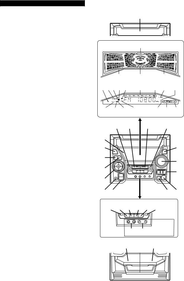
Figure 2 AC POWER SUPPLY CORD
– 2 –

CD-BP2000W/210W/2000A/BK2000W/210W
FOR A COMPLETE DESCRIPTION OF THE OPERATION OF THIS UNIT, PLEASE REFER TO THE OPERATION MANUAL.
SPECIFICATIONS
CD-BP2000W/BK2000W/BP2000A/BP210W/BK210W
 General
Power source: |
AC 110/127/220/230-240 V, |
Power consump- |
50/60 Hz |
|
|
tion: |
154 W |
Dimensions: |
Width; 270 mm (10-5/8") |
|
Height; 330 mm (13") |
|
Depth; 355 mm (14") |
Weight: |
(CD-BP2000W/BK2000W/ |
|
BP210W/BK210W) |
|
8.7 kg (19.1 lbs.) |
Weight: |
(CD-BP2000A) |
|
8.6 kg (19.0 lbs.) |
 Amplifier section
Output power: |
(CD-BP2000W/BK2000W) |
|
MPO; 334 W (167 W + 167 W) (10 |
|
% T.H.D.) [Main speaker (woofer, |
|
tweeter and super tweeters); 134 |
|
W (67 W + 67 W), Subwoofer; 200 |
|
W (100 W + 100 W)] |
|
RMS; 200 W (100 W + 100 W) (10 |
|
% T.H.D.) [Main speaker (woofer, |
|
tweeter and super tweeters); 80 W |
|
(40 W + 40 W), Subwoofer; 120 W |
|
(60 W + 60 W)] |
|
RMS; 184 W (92 W + 92 W) (0.9 % |
|
T.H.D.) [Main speaker (woofer, |
|
tweeter and super tweeters); 74 W |
|
(37 W + 37 W), Subwoofer; 110 W |
|
(55 W + 55 W)] |
|
(CD-BP210W/BP2000A/BK210W) |
|
MPO; 334 W (167 W + 167 W) (10 |
|
% T.H.D.) [Main speaker (woofer, |
|
tweeter and super tweeter); 134 W |
|
(67 W + 67 W), Subwoofer; 200 W |
|
(100 W + 100 W)] |
|
RMS; 200 W (100 W + 100 W) (10 |
|
% T.H.D.) [Main speaker (woofer, |
|
tweeter and super tweeter); 80 W |
|
(40 W + 40 W), Subwoofer; 120 W |
|
(60 W + 60 W)] |
|
RMS; 184 W (92 W + 92 W) (0.9 % |
|
T.H.D.) [Main speaker (woofer, |
|
tweeter and super tweeter); 74 W |
|
(37 W + 37 W), Subwoofer; 110 W |
|
(55 W + 55 W)] |
Output terminals: |
Speakers; 6 ohms |
|
Headphones; 16 - 50 ohms (rec- |
|
ommended; 32 ohms) |
Input terminals: |
Video/Auxiliary (audio signal); |
|
500 mV/47 kohms |
|
(CD-BK2000W/BK210W Only) |
|
Microphone 1/2; 1 mV/600 ohms |
 Compact disc player section
Type: |
3-disc multi-play compact disc |
|
player |
Signal readout: |
Non-contact, 3-beam semi-con- |
|
ductor laser pickup |
D/A converter: |
1-bit D/A converter |
Frequency re- |
|
sponse: |
20 - 20,000 Hz |
Dynamic range: |
90 dB (1 kHz) |
Tuner section |
|
Frequency range: |
FM; 88 - 108 MHz |
|
AM; 531 - 1,602 kHz |
 Cassette deck section
|
Frequency re- |
|
|
|
sponse: |
50 - 14,000 Hz (Normal tape) |
|
|
Signal/noise ratio: |
55 dB (TAPE 1, playback) |
|
|
|
|
50 dB (TAPE 2, recording/ |
|
|
|
playback) |
|
Wow and flutter: |
0.3 % (WRMS) |
|
|
|
|
|
|
CP-BP2000 |
|
|
|
Type: |
5-way type [13 cm (5-1/4") sub- |
|
|
|
|
woofer, 13 cm (5-1/4") woofer, |
|
|
|
5 cm (2") tweeter and super tweet- |
|
|
|
er 2] |
|
Maximum input |
|
|
|
power (total): |
200 W |
|
|
Rated input power |
|
|
|
(total): |
100 W |
|
|
Impedance: |
6 ohms |
|
|
Dimensions: |
Width; 310 mm (12-3/16") |
|
|
|
|
Height; 330 mm (13") |
|
|
|
Depth; 270 mm (10-5/8") |
|
Weight: |
5.3 kg (11.7 lbs.)/each |
|
|
|
|
|
|
CP-BP210 |
|
|
|
Type: |
4-way type [16 cm (6-5/16") sub- |
|
|
|
|
woofer, 10 cm (3-15/16") woofer, |
|
|
|
5 cm (2") tweeter and super tweet- |
|
|
|
er] |
|
Maximum input |
|
|
|
power (total): |
200 W |
|
|
Rated input power |
|
|
|
(total): |
100 W |
|
|
Impedance: |
6 ohms |
|
|
Dimensions: |
Width; 250 mm (9-13/16") |
|
|
|
|
Height; 330 mm (13") |
|
|
|
Depth; 240 mm (9-7/16") |
|
Weight: |
4.9 kg (10.8 lbs.)/each |
|
|
|
|
|
|
CP-BP2000A |
|
|
|
Type: |
4-way type [13 cm (5-1/4") sub- |
|
|
|
|
woofer, 13 cm (5-1/4") woofer, 5 |
|
|
|
cm (2") tweeter and super tweeter] |
|
Maximum input |
200 W |
|
|
power (total): |
|
|
|
Rated input power |
100 W |
|
|
(total): |
|
|
|
Impedance: |
6 ohms |
|
|
Dimensions: |
Width; 270 mm (10-5/8") |
|
|
|
|
Height; 330 mm (13") |
|
|
|
Depth; 264.6 mm (10-3/8") |
|
Weight: |
4.7 kg (10.3 lbs.)/each |
|
Specifications for this model are subject to change without prior notice.
– 3 –
CD-BP2000W/210W/2000A/BK2000W/210W
NAMES OF PARTS
CD-BP2000W/210W/2000A/BK2000W/210W
 Front panel
1.(CD) Disc Tray
2.Extra Bass Indicator
3.Spectrum Analyzer/Volume Level Indicator
4.(CD) Disc Number Indicators
5.Karaoke Maker Indicator
6.(CD/TUNER) Memory Indicator
7.(CD) Pause Indicator
8.(TAPE 2) Record Indicator
9.(CD) Play Indicator
10.(CD) Music Schedule Indicators
11.(CD) More Tracks Indicator
12.Sleep Indicator
13.FM Stereo Mode Indicator
14.(TAPE) Reverse Mode Indicator
15.(TAPE 2) Reverse Play Indicator
16.(TAPE 1) Play Indicator
(TAPE 2) Forward Play Indicator
17.(CD) Repeat Indicator
18.FM Stereo Indicator
19.Timer Record Indicator
20.Timer Play Indicator
21.Memory/Set Button
22.(CD) Track Down/Review Button (TUNER) Preset Down Button (TAPE 2) Fast Wind Button
23.(CD) Track Up/Cue Button (TUNER) Preset Up Button (TAPE 2) Fast Wind Button
24.Equalizer Mode Selector Button
25.Timer Set Indicator
26.On/Stand-by Button
27.Clock Button
28.Timer/Sleep Button
29.Function Selector Buttons
30.Headphone Socket
31.Dimmer Button
32.Volume Control
33.(CD) Disc Number Select Buttons
34.Tuning and Time Up/Down Buttons
35.(CD) Disc Skip Button
36.(CD) Open/Close Button
37.(TAPE 2) Record Pause Button
38.(TAPE 2) Reverse Play Button
39.(CD/TAPE) Stop Button
40.(TAPE 2) Reverse Mode Button
41.(CD) Play/Repeat Button (TAPE 1) Play Button
(TAPE 2) Forward Play Button
42.Extra Bass/Demo Mode Button
43.Microphone Sockets (BK2000W/BK210W Only)
44.Microphone Level Controls (BK2000W/BK210W Only)
45.(TAPE 1) Cassette Compartment
46.(TAPE 2) Cassette Compartment
1
2
3 |
|
4 |
3 |
5 6 7 8 |
9 |
10 |
11 12 13 |
14 15 16 17 |
|
18 19 20 |
||
|
21 |
22 |
23 |
24 |
25 |
|
|
|
|
26 |
|
|
|
31 |
27 |
|
|
|
32 |
|
|
|
|
|
28 |
|
|
|
33 |
|
|
|
|
|
29 |
|
|
|
|
30 |
34 |
|
|
35 36 |
|
37 38 39 40 41 42 |
|||
|
BK2000W/ |
43 44 |
BK210W |
ONLY |
|
45 |
46 |
– 4 –
Rear panel
1.AC Voltage Selector
2.AC Power Lead
3.FM 75 Ohms Aerial Terminal
4.FM Aerial Earth Terminal
5.AM Loop Aerial Input Socket
6.Speaker Terminals
7.Span Selector Switch
8.Video/Auxiliary (Audio Signal) Input Sockets
Speaker
CP-BP2000
1.Super Tweeters
2.Tweeter
3.Bass Reflex Duct
4.Woofer
5.Subwoofer
6.Main Speaker (Woofer, Tweeter and Super Tweeters) Wire
7.Subwoofer Wire
CP-BP210
1.Woofer
2.Tweeter
3.Super Tweeter
4.Subwoofer
5.Bass Reflex Ducts
6.Main Speaker (Woofer, Tweeter and Super Tweeter) Wire
7.Subwoofer Wire
CD-BP2000W/210W/2000A/BK2000W/210W
|
3 |
|
4 |
1 |
5 |
6 |
|
|
7 |
2 |
8 |
1 |
4 |
|
2 |
|
|
|
|
|
3 |
5 |
6 |
|
|
|
|
|
7 |
1 |
|
3 |
2 |
|
|
|
4 |
|
|
|
|
|
|
6 |
|
5 |
7 |
|
|
CP-BP2000A
1.Super Tweeter
2.Tweeter
3.Bass Reflex Duct
4.Woofer
5.Subwoofer
6.Main Speaker (Woofer, Tweeter and Super Tweeter) Wire
7.Subwoofer Wire
1
2
3
4 |
|
5 |
6 |
|
|
|
7 |
– 5 –
CD-BP2000W/210W/2000A/BK2000W/210W
CD-BP2000W/BP210W/BP2000A
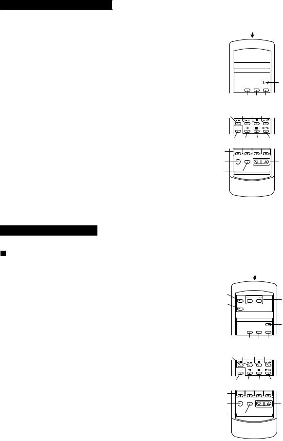
 Remote control
1.Remote Control Transmitter LED
2.(CD) Disc Skip Button
3.(CD) Clear Button
4.(CD) Memory Button
5.(CD) Random Button
6.(TAPE 2) Record Pause Button
7.(CD) Track Down/Review Button (TUNER) Preset Down Button (TAPE 2) Fast Wind Button
8.(CD) Pause Button
9.(CD) Track Up/Cue Button (TUNER) Preset Up Button (TAPE 2) Fast Wind Button
10.Equalizer Mode Selector Button
11.(TAPE 2) Reverse Play Button
12.(CD/TAPE) Stop Button
13.(CD) Play/Repeat Button (TAPE 1) Play Button
(TAPE 2) Forward Play Button
14.Function Selector Buttons
15.On/Stand-by Button
16.Extra Bass Button
17.Volume Up/Down Buttons
CD-BK2000W/BK210W
Remote control
1.Remote Control Transmitter LED
2.Karaoke Mode Button
3.Vocal Replacer Button
4.Echo Level Up/Down Buttons
5.(CD) Disc Skip Button
6.(CD) Clear Button
7.(CD) Memory Button
8.(CD) Random Button
9.(TAPE 2) Record Pause Button
10.(CD) Track Down/Review Button (TUNER) Preset Down Button (TAPE 2) Fast Wind Button
11.(CD) Pause Button
12.(CD) Track Up/Cue Button (TUNER) Preset Up Button (TAPE 2) Fast Wind Button
13.Equalizer Mode Selector Button
14.(TAPE 2) Reverse Play Button
15.(CD/TAPE) Stop Button
16.(CD) Play/Repeat Button (TAPE 1) Play Button
(TAPE 2) Forward Play Button
17.Function Selector Buttons
18.On/Stand-by Button
19.Extra Bass Button
20.Volume Up/Down Buttons
1
2
3 4 5
6 7 8 9
14 |
10 11 12 13 |
|
17 |
||
15 |
||
16 |
|
1
2 |
4 |
|
3 |
||
|
||
|
5 |
|
|
6 7 8 |
|
|
9 10 1112 |
|
17 |
13 14 15 16 |
|
|
||
18 |
20 |
|
19 |
|
– 6 –
CD-BP2000W/210W/2000A/BK2000W/210W
OPERATION MANUAL
 AM/FM interval (span)
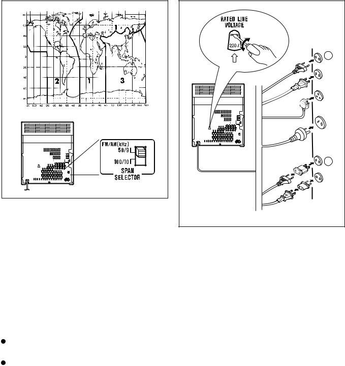
The International Telecommunication Union (ITU) has established that member countries should maintain either a 10 kHz or a 9 kHz interval between broadcasting frequencies of any AM station. The illustration shows the 9 kHz interval zones (regions 1 and 3), and the 10 kHz interval zone (region 2).
Before using the unit, set the SPAN SELECTOR switch (on the rear panel) to AM tuning interval (span) of your area.
To change the tuning zone:
1 Press the ON/STAND-BY button to enter the standby mode.
2 Set the SPAN SELECTOR switch to "50/9" for 9 kHz AM interval (50 kHz FM interval), and "100/10" for 10 kHz AM interval (100 kHz FM interval).
3 Whilst pressing down the  button and the X-BASS/ DEMO button, hold down the ON/STAND-BY button for at least 1 second.
"CLEAR AL" will appear.
Caution:
The operation explained above will erase all data stored in memory including clock and timer settings, and tuner and CD presets.
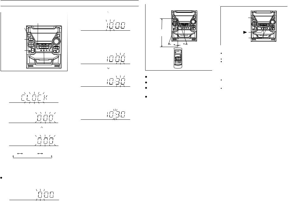
 Connecting the AC power lead
1 |
2 |
To an AC socket |
Check the setting of the AC voltage selector located on the rear panel before plugging the unit into an AC socket. If necessary, adjust the selector to correspond to the AC power voltage used in your area.
Selector adjustment:
Turn the selector with a screwdriver until the appropriate voltage number appears in the window (110 V, 127 V, 220 V or 230 V - 240 V AC).
Notes:
 Plug the AC power lead into an AC socket, after any connections.
 Unplug the AC power lead from the AC socket if the unit will not be in use for a prolonged period of time.
 AC Plug Adaptor
In areas (or countries) where an AC socket as shown in illustration  is used, connect the unit using the AC plug adaptor supplied with the unit, as illustrated. The AC plug adaptor is not included in areas where the AC wall socket and AC power plug can be directly connected (see illustration
  ).
).
– 7 –
– 8 –
SETTING THE CLOCK
(Main unit operation)
MEMORY/SET
ON/
STAND-BY
CLOCK
TUNING/ TIME
( )
)
In this example, the clock is set for the 24-hour (0:00) system.
1 Press the ON/STAND-BY button to enter the standby mode.
2 Press the CLOCK button.
3 Within 5 seconds, press the MEMORY/SET button.
4 Press the TUNING/TIME ( or ) button to select the time display mode.
0:00 AM 0:00 AM 12:00
"0:00"  The 24-hour display will appear. (0:00 - 23:59)
"AM 0:00"  The 12-hour display will appear. (AM 0:00 - PM 11:59)
"AM 12:00" The 12-hour display will appear. (AM 12:00 - PM 11:59)
Note that this can only be set when the unit is first installed or it has been reset (see page 29).
5 Press the MEMORY/SET button.
6 Press the TUNING/TIME ( or  ) button to adjust the hour.
 Press the TUNING/TIME (
 or
or  ) button once to advance the time by 1 hour. Hold it down to advance continuously.
 When the 12-hour display is selected, "AM" will change automatically to "PM".
7 Press the MEMORY/SET button.
8 Press the TUNING/TIME ( or  ) button to adjust the minutes.
 Press the TUNING/TIME (
 or
or  ) button once to advance the time by 1 minute. Hold it down to change the time in 5 - minute intervals.
 The hour setting will not advance even if minutes advance from "59" to "00".
9 Press the MEMORY/SET button.
 The clock starts operating from "0" second. (Seconds are not displayed.) And then the clock display will disappear after a few seconds.
To see the time display:
Press the CLOCK button.
 The time display will appear for about 5 seconds.
Note:
 The clock display will flash on and off at the push of the CLOCK button when the AC power supply is restored after a power failure occurs or after the AC power lead is disconnected. If this happens, follow the procedure below to change the clock time.
To change the clock time:
1Press the CLOCK button.
2Within 5 seconds, press the MEMORY/SET button.
3Perform steps 6 - 9 above.
To change the time display mode:
1Perform steps 1 - 2 in "RESETTING THE MICROCOMPUTER", on page 29.
2Perform steps 1 - 9 above.
 Remote control
0.2 m - 6 m (8" - 20')
15 |
15 |
Notes concerning use:
Replace the batteries if the operating distance is reduced or if the operation becomes erratic.
Periodically clean the transmitter LED on the remote control and the sensor on the main unit with a soft cloth.
Exposing the sensor on the main unit to strong light may interfere with operation. Change the lighting or the direction of the unit.
Keep the remote control away from moisture, excessive heat, shock, and vibrations.
RESETTING THE MICROCOMPUTER
ON/
STAND-BY
X-BASS/
DEMO
Reset the microcomputer under the following conditions:
To erase all of the stored memory contents (clock and timer settings, and tuner and CD presets).
If the display is not correct.
If the operation is not correct.
1 Press the ON/STAND-BY button to enter the standby mode.
2 Whilst pressing down the  button and the X-BASS/ DEMO button, hold down the ON/STAND-BY button for at least 1 second.
"CLEAR AL" will appear.
Caution:
The operation explained above will erase all data stored in memory including clock and timer settings, and tuner and CD presets.
BP2000W/210W/2000A/BK2000W/210W-CD
CD-BP2000W/210W/2000A/BK2000W/210W
DISASSEMBLY
Caution on Disassembly
Follow the below-mentioned notes when disassembling the unit and reassembling it, to keep it safe and ensure excellent performance:
1.Take cassette tape and compact disc out of the unit.
2.Be sure to remove the power supply plug from the wall outlet before starting to disassemble the unit.
3.Take off nylon bands or wire holders where they need to be removed when disassembling the unit. After servicing the unit, be sure to rearrange the leads where they were before disassembling.
4.Take sufficient care on static electricity of integrated circuits and other circuits when servicing.
CD-BP2000W/210W/2000A/BK2000W/210W
(A1)x2
Top Cabinet
ø3x12mm
Side Panel (Right)
(B1)x2
ø3x10mm |
(A1)x2 |
ø3x12mm
CD-BP2000W/210W/2000A/BK2000W/210W
STEP |
REMOVAL |
|
PROCEDURE |
|
FIGURE |
|
|
|
|
|
|
1 |
Top Cabinet |
1. |
Screw ..................... |
(A1) x4 |
9-1 |
|
|
|
|
|
|
2 |
Side Panel |
1. |
Screw ..................... |
(B1) x8 |
9-1 |
|
(Left/right) |
|
|
|
|
|
|
|
|
|
|
3 |
CD Player Unit/ |
1. |
Turn on the power supply, |
9-2 |
|
|
CD Tray Cover |
|
open the disc tray, take out |
|
|
|
|
|
the CD cover, and close. |
|
|
|
|
|
(Note 1) |
|
|
|
|
2. |
Screw ..................... |
(C1) x1 |
|
|
|
3. |
Hook ....................... |
(C2) x3 |
|
|
|
4. |
Hook ....................... |
(C3) x2 |
|
|
|
5. |
Socket .................... |
(C4) x2 |
|
|
|
|
|
|
|
4 |
Rear Panel |
1. |
Screw ..................... |
(D1) x10 |
9-2 |
|
|
|
|
|
|
5 |
Main PWB |
1. |
Screw ..................... |
(E1) x3 |
9-2 |
|
|
2. |
Socket .................... |
(E2) x4 |
10-2 |
|
|
3. |
Flat Cable ............... |
(E3) x1 |
|
|
|
4. |
Tip Wire .................. |
(E4) x1 |
|
|
|
|
|
|
|
6 |
Power Supply PWB |
1. |
Screw ..................... |
(F1) x2 |
10-2 |
|
|
2. |
Socket .................... |
(F2) x4 |
|
|
|
3. |
Flat Wire ................. |
(F3) x1 |
10-3 |
|
|
|
|
|
|
7 |
Karaoke PWB |
1. |
Screw ..................... |
(G1) x2 |
10-3 |
|
BK2000W/210W Only |
|
|
|
|
8 |
Front Panel |
1. |
Screw ..................... |
(H1) x2 |
10-2 |
|
|
|
|
|
|
9 |
Display PWB |
1. Screw ..................... |
(J1) x13 |
10-4 |
|
|
|
2. |
Socket .................... |
(J2) x1 |
|
|
|
|
|
|
|
10 |
Tape Mechanism |
1. |
Open the cassette holder. |
10-4 |
|
|
|
2. |
Screw...................... |
(K1) x5 |
|
|
|
|
|
|
|
11 |
Headphones PWB |
1. |
Screw ..................... |
(L1) x1 |
10-4 |
12 |
Turntable |
1. |
Hook ....................... |
(M1) x2 |
10-5 |
|
|
2. |
Cover ..................... |
(M2) x1 |
|
13 |
Disc Tray |
1. |
Turn fully the lock lever in the |
9-3 |
|
|
|
|
arrow direction. |
|
|
|
|
2. |
While holding the lock lever,rotate |
10-1 |
|
|
|
|
the cam gear until the cam gear |
|
|
|
|
|
rib engages with the clamp lever. |
|
|
|
|
3. |
Push the slide holder backward to |
10-6 |
|
|
|
|
engage the claw with the groove |
|
|
|
|
|
and remove it in the direction |
|
|
|
|
|
of the arrow. .............. |
(N1) x6 |
|
|
|
|
|
|
|
14 |
CD Servo PWB |
1. |
Screw ..................... |
(P1) x1 |
11-1 |
|
(Note 2) |
2. |
Hook ....................... |
(P2) x2 |
|
|
|
3. |
Socket .................... |
(P3) x4 |
|
|
|
|
|
|
|
15 |
CD Mechanism |
1. |
Hook ....................... |
(Q1) x2 |
11-2 |
|
|
2. |
Hook ....................... |
(Q2) x3 |
|
|
|
|
|
|
|
16 |
Loading Motor PWB |
1. |
Hook ....................... |
(R1) x5 |
11-2 |
Note 1:
How to open the changer manually. (Fig. 9-3)
1.In this state, turn fully the lock lever in the arrow direction through the hole on the loading chassis bottom.
2.While holding the lock lever, rotate the cam gear anticlockwise until the cam gear rib engages with the clamp lever. (Fig. 10-1)
3.After that, push forward the CD slide holder.
|
|
|
Side Panel |
|
|
|
(Left) |
(B1)x4 |
|
|
(B1)x2 |
ø3x10mm |
|
|
|
|
|
ø3x10mm |
|
|
Rear |
|
|
|
|
|
|
|
Panel |
|
|
|
Figure 9-1 |
|
|
CD Servo |
|
CD Tray Cover |
|
PWB |
(C4)x2 |
|
(C2) x3 |
|
|
|
|
|
|
1 |
|
(C3) x1 |
|
|
|
Pull |
|
|
1 |
|
|
|
2 |
|
|
|
CD Player |
Rear |
|
|
Unit |
|
|
|
|
Panel |
|
|
(C3)x1 |
(C1)x1 |
|
|
(E1)x1 |
ø3x10mm |
|
|
ø3x6mm |
(D1)x8 |
|
|
(E1)x2 |
|
|
ø3x10mm |
|
ø3x10mm |
|
(D1)x2 |
|
|
|
||
|
Main PWB |
ø3x10mm |
|
Lock Lever
Note 2:
1.After removing the connector for the optical pickup from the connector, wrap the conductive aluminium foil around the front end of the connector remove to protect the optical pickup from electrostatic damage.
Note 3:
1.Be careful not to break the claw of the CD mechanism.
2.When fining back the cam gear assembly, let it lock by front movement.
– 9 –
CD-BP2000W/210W/2000A/BK2000W/210W
Clamp Lever
|
(J1)x13 |
|
ø3x10mm |
|
Tape |
|
Mechanism |
Cam Gear Rib |
(K1)x5 |
|
ø3x10mm |
|
(L1)x1 |
|
ø3x10mm |
Figure 10-1
(F1)x1 |
(F1)x1 |
ø3x6mm |
|
|
ø3x10mm |
CDBK2000W/
BK210W ONLY
(E2)x1
(E2)x2
(E4)x1(E3)x1
Power
Supply
PWB
Main PWB
(F2)x1
(M1) x2
|
|
(E2)x1 |
|
(F2)x3 |
(H1)x2 |
Power |
|
Supply |
|||
|
|
ø3x10mm PWB
Figure 10-2
CD-BK2000W/ |
Display PWB |
|
BK210W ONLY |
||
|
||
Karaoke |
|
|
PWB |
|
2
1
(G1)x2
ø3x10mm
Tape Mechanism
Figure 10-3
– 10 –
(J2)x1
Display PWB
(F3)x1
Headphones
PWB
 Open
Open
Cassette
Holder
Figure 10-4
(M2) x1
Turntable
Disc Tray
CD Player Unit
Figure 10-5
(N1) x3
3
(N1) x3
Figure 10-6
CD-BP2000W/210W/2000A/BK2000W/210W
|
|
|
CD |
(Q2) x3 |
|
(P1)x1 |
CD Servo |
CD Player |
Mechanism |
|
|
ø3x8mm |
|
|
|
||
Base |
|
|
|
||
PWB |
|
|
|
||
|
|
|
|
|
|
|
(P3) x2 |
|
|
|
|
(P2) x2 |
|
|
|
|
Loading |
|
|
|
(Q1) x1 |
Motor |
|
|
|
|
(Q1) x1 |
PWB |
(P3) x2
(R1) x5
Figure 11-1
Figure 11-2
CP-BP2000
STEP |
REMOVAL |
|
PROCEDURE |
|
FIGURE |
|
|
|
|
|
|
|
|
1 |
Front Panel |
1. |
Front Panel |
|
|
11-3 |
............ |
|
|||||
|
|
2. Tip |
|
(A1) x4 |
11-4 |
|
|
|
|
||||
|
|
|
|
|
|
|
2 |
Woofer |
1. |
Screw ..................... |
(B1) x4 |
11-5 |
|
|
|
|
|
|
|
|
3 |
Subwoofer |
1. |
Screw ..................... |
(C1) x4 |
11-5 |
|
|
|
2. |
Sub Woofer Ring ... |
(C2) x1 |
|
|
|
|
|
|
|
|
|
4 |
Tweeter |
1. |
Screw ..................... |
(D1) x2 |
11-5 |
|
|
|
|
|
|
|
|
5 |
Super Tweeter |
1. Screw ..................... |
(E1) x4 |
11-4 |
||
|
|
|
|
|
|
|
Super
Tweeter
(E1)x4
ø3x10mm
Woofer
(A1)x4 |
|
|
|
(B1)x4 |
|
|
ø4x16mm |
|
|
(C2)x1 |
|
Front Panel |
(C1)x4 |
|
ø4x20mm |
||
|
Screw
Driver should
Driver
be pried away from Speaker Box.
Figure 11-3
Figure 11-4
Sub Woofer
(D1)x2 |
Tweeter |
|
ø3x10mm |
||
Figure 11-5 |
||
|
– 11 –
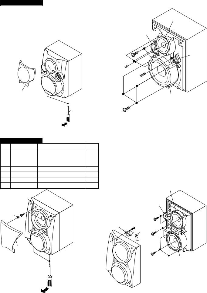
CD-BP2000W/210W/2000A/BK2000W/210W
CP-BP210
STEP |
REMOVAL |
|
PROCEDURE |
|
FIGURE |
|
|
|
|
|
|
1 |
Front Panel |
1. Net .......................... |
(A1) x1 |
12-1 |
|
|
|
|
|
|
|
2 |
Woofer |
1. Screw ..................... |
(B1) x4 |
12-2 |
|
|
|
|
|
|
|
3 |
Subwoofer |
1. |
Screw .................... |
(C1) x4 |
12-2 |
|
|
|
|
|
|
4 |
Tweeter |
1. |
Screw .................... |
(D1) x2 |
12-2 |
|
|
|
|
|
|
5 |
Super Tweeter |
1. |
Screw .................... |
(E1) x2 |
12-2 |
|
|
|
|
|
|
(A1)x1
|
|
|
Screw |
|
|
|
|
|
Driver |
|
|
|
|
|
Driver should |
|
|
|
|
|
be pried away |
|
|
|
|
|
from Speaker |
|
|
|
|
|
Box. |
|
|
|
|
Figure 12-1 |
|
|
|
|
CP-BP2000A |
|
|
|
|
STEP |
REMOVAL |
|
PROCEDURE |
|
FIGURE |
1 |
Front Panel |
1. Net .......................... |
(A1) x1 |
12-3 |
|
|
|
2. |
Rubber ................... |
(A2) x4 |
|
|
|
3. |
Screw ..................... |
(A3) x4 |
|
|
|
4. |
Tip .......................... |
(A4) x2 |
12-4 |
2 |
Woofer |
1. |
Screw ..................... |
(B1) x4 |
12-4 |
3 |
Subwoofer |
1. |
Screw .................... |
(C1) x4 |
12-4 |
4 |
Tweeter |
1. |
Screw .................... |
(D1) x2 |
12-4 |
5 |
Super Tweeter |
1. |
Screw .................... |
(E1) x2 |
12-4 |
|
Front |
|
|
|
|
|
Panel |
|
|
|
|
(A3)x4 |
|
|
|
|
|
ø4x20mm |
|
|
|
|
|
(A2)x4 |
|
|
|
|
|
(A1)x1
Screw
 Driver
Driver should be pried away from Speaker Box.
Woofer
Tweeter
(D1)x2 Ø3x10mm
Super Tweeter
(B1)x4  Ø4x16mm
(E1)x2 
Ø3x10mm
Sub Woofer
(C1)x4
Ø4x16mm
Figure 12-2
Woofer
Tweeter
(D1)x2
ø3x10mm
Super (E1)x2
Tweeter ø3x10mm
(A4)x2
(B1)x4
ø4x16mm
(C1)x4 |
|
ø4x16mm |
Subwoofer |
Figure 12-3 |
Figure 12-4 |
– 12 –
CD-BP2000W/210W/2000A/BK2000W/210W
REMOVING AND REINSTALLING THE MAIN PARTS
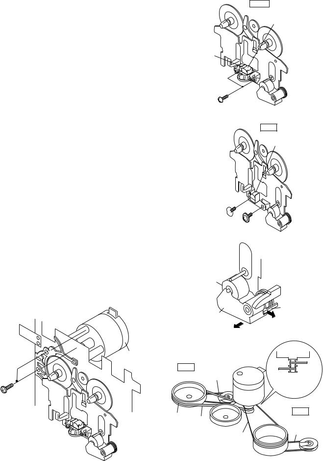
TAPE MECHANISM SECTION
Perform steps 1 to 8 and 10 of the disassembly method to remove the tape mechanism.
How to remove the record/playback and erase heads (TAPE 2) (See Fig. 13-1)
1.When you remove the screw (A1) x 2 pcs., the recording/ playback head and three-dimensional head of the erasing head can be removed.
How to remove the playback head (TAPE 1) (See Fig. 13-2)
1.When you remove the screw (B1) x 2 pcs., the playback head.
How to remove the pinch roller (Tape 1/2) (See Fig. 13-3)
1.Carefully bend the pinch roller pawl in the direction of the arrow <A>, and remove the pinch roller (C1) x 1 pc., in the
direction of the arrow <B>.
Note:
When installing the pinch roller, pay attention to the spring mounting position.
How to remove the belt (TAPE 1) (See Fig. 13-4)
1.Remove the main belt (D1) x 1 pc., from the motor side.
2.Remove the FF/REW belt (D2) x 1 pc.
TAPE2
Record/Playback
Head
Erase Head
(A1)x2
Ø2x6mm
Figure 13-1
TAPE1
Playback
Head
(B1)x1 
Ø2x9mm (B1)x1
Ø2x5mm
How to remove the belt (TAPE 2) (See Fig. 13-4)
Figure 13-2
1.Remove the main belt (E1) x 1 pc., from the motor side.
2.Remove the FF/REW belt (E2) x 1 pc.
How to remove the motor (See Fig. 13-5)
1. Remove the screws (F1) x 2 pcs., to remove the motor.
|
Pinch |
|
Roller |
Pinch Roller |
Pawl |
|
(C1)x1 |
Pull <A> |
|
|
|
|
Pull |
|
|
|
|
<B> |
|
|
|
|
Figure 13-3 |
|
|
Motor |
|
|
Motor |
|
TAPE2 |
FF/REW |
Motor |
|
TAPE1 |
|
|
|||
|
Belt |
TAPE2 |
|
Main Belt |
|
(E2)x1 |
|
(D1)x1 |
|
|
Main Belt |
|||
|
|
|
||
|
|
(E1)x1 |
|
|
(F1) x2 |
|
|
|
|
Ø2.6x5mm |
|
|
|
|
Main Belt |
|
|
|
TAPE1 |
(E1)x1 |
|
|
FF/REW |
|
|
|
|
||
|
|
|
|
|
|
|
|
|
Belt |
|
|
(D1)x1 |
|
(D2)x1 |
|
|
|
|
|
Figure 13-5 |
|
Figure 13-4 |
|
|
– 13 –
CD-BP2000W/210W/2000A/BK2000W/210W
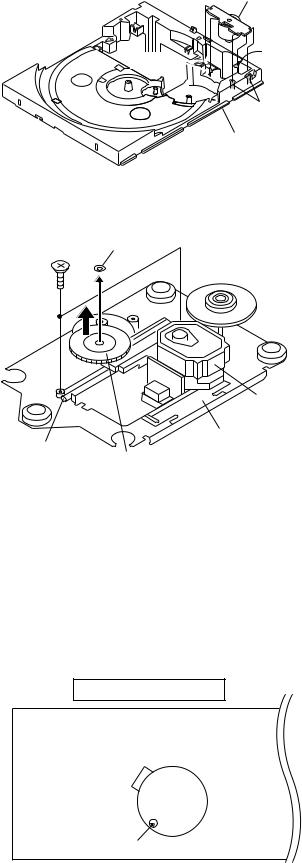
CD MECHANISM SECTION
Perform steps 1, 2, 3, 12, 13, 14 and 15 of the disassembly method to remove the CD mechanism.
How to remove the loading motor (See Fig. 14-1)
1. Bend the hooks (A1) x 5 pcs., to remove the loading motor.
Loading Motor
(A1)x1
(A1)x2
(A1)x2
CD Base
Figure 14-1
How to remove the pickup (See Fig. 14-2)
1.Remove the stop washer (B1) x 1 pc., to remove the gear (B2) x 1 pc.
2.Remove the screws (B3) x 2 pcs., to remove the shaft (B4)x 1 pc.
3.Remove the pickup.
Note
After removing the connector for the optical pickup from the connector, wrap the conductive aluminium foil around the front end of connector remove to protect the optical pickup from electrostatic damage.
(B3) x2 |
Stop Washer |
|
(B1) x1 |
||
ø2.6 x6mm |
||
|
Pickup
Shaft |
CD Mechanism |
|
Gear |
||
(B4) x1 |
||
(B2) x1 |
||
|
||
|
Figure 14-2 |
ADJUSTMENT
MECHANISM SECTION
∙ Driving Force Check
Torque Meter |
Specified Value |
|
|
Play: TW-2111 |
Tape 1: Over 80 g |
|
Tape 2: Over 80 g |
|
|
∙ Torque Check
Torque Meter |
Specified Value |
|
|
|
|
|
Tape 1 |
Tape 2 |
|
|
|
Play: TW-2111 |
30 to 80 g. cm |
30 to 80 g.cm |
|
|
|
Fast forward: TW-2231 |
— |
70 to 180 g.cm |
|
|
|
Rewind: TW-2231 |
— |
70 to 180 g.cm |
|
|
|
∙ Tape Speed
|
Test Tape |
Adjusting |
Specified |
Instrument |
|
|
Point |
Value |
Connection |
|
|
|
|
|
Normal |
MTT-111 |
Variable |
3,000 ± |
Speaker |
speed |
|
Resistor in |
30 Hz |
terminal |
|
|
motor. |
|
(Load |
|
|
(MM1) |
|
resistance: |
|
|
|
|
6 ohms) |
|
|
|
|
|
TAPE MECHANISM
MM1
 Motor
Motor
Variable Resistor in motor
Figure 14-3
– 14 –
TUNER SECTION
fL: Low-range frequency fH: High-range frequency
∙ AM IF/RF
Signal generator: 400 Hz, 30%, AM modulated
Test Stage |
Frequency |
Frequency |
Setting/ |
Instrument |
|
|
Display |
Adjusting |
Connection |
|
|
|
Parts |
|
|
|
|
|
|
AM IF |
450 kHz |
1,602 kHz |
T351 |
*1 |
|
|
|
|
|
AM Band |
— |
531 kHz |
(fL): T306 |
*2 |
Coverage |
|
|
1.1 ± 0.1 V |
|
|
|
|
|
|
AM Tracking |
990 kHz |
990 kHz |
(fL): T303 |
*1 |
|
|
|
|
|
CD-BP2000W/210W/2000A/BK2000W/210W
∙ FM RF
Signal generator: 1 kHz, 40 kHz dev., FM modulated
Test Stage |
Frequency |
Frequency |
Serring/ |
Instrument |
|
|
|
|
Display |
Adjusting |
Connection |
|
|
|
|
Point |
|
|
|
|
|
|
|
FM Band |
— |
|
87.50 MHz |
T301(fL); |
*1 |
Coverage |
|
|
|
1.3 V ± 50 mV |
|
|
|
|
|
|
|
FM RF |
98.00 MHz |
98.00 MHz |
L312 |
*2 |
|
|
(10-30 dB) |
|
|
|
|
|
|
|
|
|
|
*1. Input: Antenna, |
Output: TP301 |
|
|||
*2. Input: Antenna, |
Output: Speaker terminal |
|
|||
*1. Input: Antenna, |
Output: TP302 |
*2. Input: Antenna, |
Output: TP301 |
MAIN PWB
|
CNP302 |
|
SO302 |
AM LOOP |
|
ANTENNA |
||
FM ANTENNA |
||
|
||
|
1 |
|
|
IC301 |
TP301
|
AM |
T303 |
R381 |
|
|
TRACKING fL |
|
|
|
|
|
T302 |
L312 |
|
T306 |
|
T301 |
FM IF |
|
FM BAND |
1 |
AM BAND |
COVERAGE fL |
COVERAGE fL |
|
T351 |
|
IC303 |
|
|
TP302 |
AM IF |
|
R357 |
Figure 15-1 ADJUSTMENT POINT
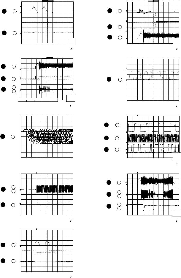
CD SECTION
Adjustment
Since this CD system incorporates the following automatic adjustment functions, readjustment is not needed when replacing the pickup. Therefore, different PWBs and pickups can be combined freely.
Each time a disc is changed, these adjustments are performed automatically. Therefore, playback of each disc can be performed under optimum conditions.
Items adjusted automatically
(1)Offset adjustment (The offset voltage between the head amplifier output and the VREF reference voltage is compensated inside the IC.)
*Focus offset adjustment
*Tracking offset adjustment
(2)Tracking balance adjustment (waveform drawing 15-2 EFBL)
(3)Gain adjustment (The gain is compensated inside the IC so that the loop gain at the gain crossover frequency will be 0dB.)
*Focus gain adjustment
*Tracking gain adjustment
|
Stopped |
|
T |
|
|
|
|
|
1999/04/05 |
20:26:47 |
|
|
|
|
|
|
|
|
|||
|
CH1=500mV |
CH2=200mV |
CH3=1V |
|
|
500ms/div |
||||
|
DC |
10:1 |
|
DC |
10:1 |
DC 10:1 |
|
|
(500ms/div) |
|
|
|
|
|
|
|
|
|
|
NORM:20kS/s |
|
T |
FDO |
|
|
|
|
|
|
|
|
|
|
|
|
|
|
|
|
|
|
|
|
1 |
|
|
|
|
|
|
|
|
|
|
3 |
TE |
|
|
|
|
|
|
|
|
|
|
|
|
|
|
|
|
|
|
|
|
|
EFBL |
|
|
|
|
|
|
|
|
|
2 |
|
|
|
|
|
|
|
|
|
|
|
|
|
|
|
|
|
|
|
|
CH2 |
|
|
|
|
|
|
|
|
|
|
v/DIV |
|
|
|
|
|
|
|
|
|
|
200mV |
|
=Filter= |
|
|
=Offset= |
=Record Length= |
|
=Trigger= |
|||
Smoothing : ON |
CH1 : |
0.000V |
Main : |
100K |
Mode : SINGLE |
|||||
BW |
: FULL |
|
CH2 : |
0.000V |
Zoom : |
2k |
Type |
: EDGE CH1 |
||
|
|
|
CH3 : |
0.00V |
|
|
Delay : |
0.0ns |
||
|
|
|
CH4 : |
0.00V |
|
|
Hold off : |
0.2us |
||
|
|
|
|
|
Figure 15-2 |
|
|
|
||
CD ERROR CODE DESCRIPTION
Error |
State Code |
|
|
|
[Servo System Error] |
0001 |
Cannot detect Pickup-in SW |
0002 |
DSP access error |
|
|
|
[Error during close operation] |
0101 |
Open/Close SW not functioning (Low → High) |
0103 |
Open/Close SW not functioning (High → Low) |
|
|
|
[Error during open operation] |
0201 |
Open/Close SW not functioning (Low → High) |
0203 |
Open/Close SW not functioning (High → Low) |
|
|
|
[Error during skip operation] |
0302 |
Pickup-in SW is not detected |
0306 |
During Disc 1 search, Open/Close SW or Clamp SW |
|
or Disc SW do not change to low. |
0307 |
Clamp SW not function (Low → High) |
0308 |
Clamp SW not function (High → Low) |
|
|
– 15 –
CD-BP2000W/210W/2000A/BK2000W/210W
NOTES ON SCHEMATIC DIAGRAM
∙Resistor:
To differentiate the units of resistors, such symbol as K and M are used: the symbol K means 1000 ohm and the symbol M means 1000 kohm and the resistor without any symbol is ohm-type resistor. Besides, the one with “Fusible” is a fuse type.
∙Capacitor:
To indicate the unit of capacitor, a symbol P is used: this symbol P means micro-micro-farad and the unit of the capacitor without such a symbol is microfarad. As to electrolytic capacitor, the expression “capacitance/withstand voltage” is used.
(CH), (TH), (RH), (UJ): Temperature compensation (ML): Mylar type
(P.P.): Polypropylene type
∙Schematic diagram and Wiring Side of P.W.Board for this model are subject to change for improvement without prior notice.
REF. NO |
DESCRIPTION |
POSITION |
|
|
|
SW1 |
OPEN/CLOSE |
ON—OFF |
|
|
|
SW2 |
CLAMP |
ON—OFF |
|
|
|
SW3 |
DISC NUMBER |
ON—OFF |
|
|
|
SW4 |
PICKUP IN |
ON—OFF |
|
|
|
SW601 |
SPAN SELECTOR |
9kHz/50kHz |
|
|
|
SW701 |
ON/STAND-BY |
ON—OFF |
|
|
|
SW702 |
CLOCK |
ON—OFF |
|
|
|
SW703 |
TIMER |
ON—OFF |
|
|
|
SW709 |
DISC 1 |
ON—OFF |
|
|
|
SW710 |
DISC 2 |
ON—OFF |
|
|
|
SW711 |
DISC 3 |
ON—OFF |
|
|
|
SW712 |
DISC SKIP |
ON—OFF |
|
|
|
SW713 |
OPEN/CLOSE |
ON—OFF |
|
|
|
SW714 |
DIMMER |
ON—OFF |
|
|
|
SW715 |
X-BASS/MEMO |
ON—OFF |
|
|
|
SW716 |
EQUALIZER |
ON—OFF |
|
|
|
FRONT
VIEW
E |
C |
B |
(S) |
(G) |
(D) |
(1) |
(2) |
(3) |
∙The indicated voltage in each section is the one measured by Digital Multimeter between such a section and the chassis with no signal given.
1.In the tuner section, ( ) indicates AM
< > indicates FM stereo
2.In the main section, a tape is being played back.
3.In the deck section, a tape is being played back. ( ) indicates the record state.
4.In the power section, a tape is being played back.
5.In the CD section, the CD is stopped.
∙Parts marked with “ ” (
” ( 


 ) are important for maintaining the safety of the set. Be sure to replace these parts with specified ones for maintaining the safety and performance of the set.
REF. NO |
DESCRIPTION |
POSITION |
|
|
|
SW722 |
CD |
ON—OFF |
|
|
|
SW723 |
TAPE |
ON—OFF |
|
|
|
SW724 |
TUNING DOWN |
ON—OFF |
|
|
|
SW725 |
MEMORY/SET |
ON—OFF |
SW726 |
PRESET DOWN |
ON—OFF |
|
|
|
SW727 |
PRESET UP |
ON—OFF |
|
|
|
SW728 |
PLAY |
ON—OFF |
|
|
|
SW729 |
STOP |
ON—OFF |
|
|
|
SW730 |
REV PLAY |
ON—OFF |
|
|
|
SW731 |
REC/PAUSE |
ON—OFF |
|
|
|
SW732 |
TUNING/TIME UP |
ON—OFF |
|
|
|
SW733 |
VIDEO/AUX |
ON—OFF |
|
|
|
SW734 |
TUNER (BAND) |
ON—OFF |
|
|
|
SW735 |
REV MODE |
ON—OFF |
|
|
|
SW801 |
VOLTAGE SELECTOR |
230-240V |
|
|
|
FRONT
VIEW
2SC3203 Y |
KRC104 M |
4204UYT7 |
2SA1015 GR |
KTA1271 Y |
4204UGT7 |
2SC1845 F |
KTA1273 Y |
4204SRT7 |
KTC3203 Y |
KTA1274 Y |
|
KTA1266 GR |
KTC2026 |
|
KRC102 M |
KTC3199 GR |
|
KTC3194 Y |
|
|
Figure 16 TYPES OF TRANSISTOR AND LED
– 16 –
CD-BP2000W/210W/2000A/BK2000W/210W
WAVEFORMS OF CD CIRCUIT
|
|
|
Stopped |
|
|
|
|
|
|
|
|
|
|
|
CH1=500mV |
|
|
CH3=500mV |
500ms/div |
||||
|
|
|
DC |
10:1 |
|
|
|
DC 10:1 |
|
(500ms/div) |
|
|
|
T |
|
|
|
|
|
|
|
NORM:20kS/s |
|
1 |
IC2 24 |
|
FDO |
|
|
|
|
|
|
|
|
1 |
|
|
|
|
|
|
|
|
|
||
2 |
|
|
TDO |
|
|
|
|
|
|
|
|
IC2 23 |
3 |
|
|
|
|
|
|
|
|
|
|
|
|
|
|
|
|
|
|
|
|
||
|
|
|
|
|
|
|
|
|
|
|
CH1 |
|
|
|
|
|
|
|
|
|
|
|
v/DIV |
|
|
|
|
|
|
|
|
|
|
|
500mV |
|
|
|
=Filter= |
|
|
=Offset= |
=Record Length= |
=Trigger= |
|||
|
|
Smoothing : |
ON |
CH1 : |
0.000V |
Main : |
100K |
Mode : AUTO |
|
||
|
|
BW |
: FULL |
|
CH2 : |
0.0V |
Zoom : |
2K |
Type : EDGE CH1 |
||
|
|
|
|
|
CH3 : |
0.000V |
|
|
Delay : |
0.0ns |
|
|
|
|
|
|
CH4 : |
0.00V |
|
|
Hold off : |
0.2us |
|
|
|
Stopped |
|
|
|
|
|
|
|
|
|
|
|
|
CH1=500mV |
CH2=10V |
CH3=1V |
|
500ms/div |
||||
|
|
|
DC |
10:1 |
|
DC |
10:1 |
DC 10:1 |
|
(500ms/div) |
|
|
|
|
|
|
|
|
|
|
|
NORM:20kS/s |
|
1 |
IC2 24 |
1 |
FDO |
|
|
|
|
|
|
|
|
|
|
|
|
|
|
|
|
|
|
|
|
3 |
IC2 72 |
T |
DRF |
|
|
|
|
|
|
|
|
2 |
|
|
|
|
|
|
|
|
|||
|
|
|
|
|
|
|
|
|
|||
|
|
|
|
|
|
|
|
|
|
||
4 |
IC1 18 , |
|
TE |
|
|
|
|
|
|
|
|
IC2 16 |
3 |
|
|
|
|
|
|
|
|
|
|
|
|
|
|
|
|
|
|
|
|
||
|
|
|
|
|
|
|
|
|
|
|
CH2 |
|
|
|
|
|
|
CH Position To |
|
|
|
Position |
|
|
|
|
|
|
|
|
|
|
0.20div |
||
|
|
-3div |
-1div |
0div |
+1div |
+3div |
|
||||
|
|
|
|
||||||||
|
|
|
=Filter= |
|
|
=Offset= |
=Record Length= |
=Trigger= |
|||
|
|
Smoothing : |
ON |
CH1 : |
0.000V |
Main : |
100K |
Mode : AUTO |
|
||
|
|
BW |
: FULL |
|
CH2 : |
0.0V |
Zoom : |
2K |
Type : EDGE CH1 |
||
|
|
|
|
|
CH3 : |
0.00V |
|
|
Delay : |
0.0ns |
|
|
|
|
|
|
CH4 : |
0.00V |
|
|
Hold off : |
0.2us |
|
5 |
IC1 27 |
|
|
|
|
|
|
|
|
|
|
|
|
|
|
|
|
|
|
|
|
Vp-p=1.0V~1.3V |
|
|
|
|
|
|
|
|
|
|
|
0.5mV/div,0.5 sec/div |
|
|
|
Stopped |
|
|
T |
|
|
|
|
|
|
|
|
|
|
|
|
|
|
|
|
||
|
|
|
CH1=10V |
|
CH2=1V |
|
|
100ms/div |
|||
|
|
|
DC |
10:1 |
|
DC |
10:1 |
|
|
(100ms/div) |
|
|
|
|
|
|
|
|
|
|
|
NORM:100kS/s |
|
4 |
IC1 18 , |
|
TE |
|
|
|
|
|
|
|
|
|
|
|
|
|
|
|
|
|
|
||
|
2 |
|
|
|
|
|
|
|
|
|
|
IC2 16 |
|
|
|
|
|
|
|
|
|
|
|
3 |
|
T |
DRF |
|
|
|
|
|
|
|
|
IC2 72 |
1 |
|
|
|
|
|
|
|
|
|
|
|
|
|
|
|
|
|
|
|
|
||
|
|
|
=Filter= |
|
|
=Offset= |
=Record Length= |
=Trigger= |
|||
|
|
Smoothing : |
ON |
CH1 : |
0.0V |
Main : |
100K |
Mode : NORMAL |
|||
|
|
BW |
: FULL |
|
CH2 : |
0.00V |
Zoom : |
2K |
Type : EDGE CH1 |
||
|
|
|
|
|
CH3 : |
0.00V |
|
|
Delay : |
2.924ms |
|
|
|
|
|
|
CH4 : |
0.00V |
|
|
Hold off : |
0.2us |
|
|
|
Stopped |
|
|
T |
|
|
|
1999/04/07 |
09:51:15 |
|
|
|
|
|
|
|
|
|
||||
|
|
|
CH1=200mV |
CH2=500mV |
|
|
500ms/div |
||||
|
|
|
DC |
10:1 |
|
DC |
10:1 |
|
|
(500ms/div) |
|
|
|
|
|
|
|
|
|
|
|
NORM:20kS/s |
|
|
|
T |
|
|
|
|
|
|
|
|
|
1 |
IC2 24 |
|
FDO |
|
|
|
|
|
|
|
|
2 |
|
|
|
|
|
|
|
|
|
||
6 |
IC2 25 |
1 |
SPDO |
|
|
|
|
|
|
|
|
|
|
|
|
|
|
|
|
|
|||
|
|
|
|
|
|
|
|
|
|
||
|
|
|
=Filter= |
|
|
=Offset= |
=Record Length= |
=Trigger= |
|||
|
|
Smoothing : |
ON |
CH1 : |
0.000V |
Main : |
100K |
Mode : NORMAL |
|||
|
|
BW |
: FULL |
|
CH2 : |
0.000V |
Zoom : |
2K |
Type : EDGE CH2 |
||
|
|
|
|
|
CH3 : |
0.00V |
|
|
Delay : |
2.924ms |
|
|
|
|
|
|
CH4 : |
0.00V |
|
|
Hold off : |
0.2us |
|
|
|
|
|
Stopped |
|
|
|
|
|
|
1999/04/05 |
17:33:17 |
|||
|
|
|
|
|
CH1=500mV |
|
CH3=1V |
CH4=1V |
|
500ms/div |
|||||
|
|
|
|
|
DC |
10:1 |
|
|
|
DC 10:1 |
|
DC 10:1 |
(500ms/div) |
||
|
|
|
|
|
|
|
|
|
|
|
|
|
|
NORM:20kS/s |
|
7 |
|
|
|
|
PDO1 |
|
|
|
|
|
|
|
|
|
|
IC2 |
1 |
3 |
|
|
|
|
|
|
|
|
|
|
|
||
|
|
|
|
|
|
|
|
|
|
|
|
||||
|
|
|
|
4 |
|
|
|
|
|
|
|
|
|
|
|
8 |
IC2 |
2 |
|
PDO2 |
|
|
|
|
|
|
|
|
|
|
|
|
|
|
|
|
|
|
|
|
|
|
|
||||
|
|
|
|
T |
|
|
|
|
|
|
|
|
|
|
|
1 |
IC2 24 |
|
FDO |
|
|
|
|
|
|
|
|
|
|
||
1 |
|
|
|
|
|
|
|
|
|
|
CH1 |
||||
|
|
|
|
|
|
|
|
|
|
|
|
|
|
|
|
|
|
|
|
|
|
|
|
|
|
|
|
|
|
|
v/DIV |
|
|
|
|
|
|
|
|
|
|
|
|
|
|
|
500mV |
|
|
|
|
|
=Filter= |
|
|
=Offset= |
=Record Length= |
|
|
=Trigger= |
|||
|
|
|
|
Smoothing : |
ON |
|
CH1 : |
0.000V |
Main : |
100K |
Mode : AUTO |
|
|||
|
|
|
|
BW |
: FULL |
|
|
CH2 : |
0.0V |
Zoom : |
2K |
Type |
|
: EDGE CH2 |
|
|
|
|
|
|
|
|
|
CH3 : |
0.00V |
|
|
Delay : |
0.0ns |
||
|
|
|
|
|
|
|
|
CH4 : |
0.00V |
|
|
Hold off : |
0.2us |
||
|
|
|
|
Stopped |
|
T |
|
|
|
|
1999/04/07 |
09:25:28 |
|||
|
|
|
|
|
|
|
|
|
|
||||||
|
|
|
|
|
CH1=2V |
|
|
|
|
|
|
|
500ns/div |
||
|
|
|
|
|
DC |
10:1 |
|
|
|
|
|
|
|
(500ns/div) |
|
|
|
|
|
|
|
|
|
|
|
|
|
|
|
NORM:200MS/s |
|
|
|
|
|
T |
|
|
|
|
|
|
|
|
|
|
|
9 |
IC2 37 |
1 |
DOUT |
|
|
|
|
|
|
|
|
|
|
||
|
|
|
|
|
|
|
|
|
|
|
|||||
|
|
|
|
|
=Filter= |
|
|
=Offset= |
=Record Length= |
|
|
=Trigger= |
|||
|
|
|
|
Smoothing : |
ON |
CH1 : |
0.00V |
Main : |
1K |
Mode : NORMAL |
|||||
|
|
|
|
BW |
: FULL |
|
CH2 : |
0.00V |
Zoom : |
100 |
Type |
: EDGE CH1 |
|||
|
|
|
|
|
|
|
CH3 : |
0.00V |
|
|
Delay : |
2.887ms |
|||
|
|
|
|
|
|
|
CH4 : |
0.00V |
|
|
Hold off : |
0.2us |
|||
|
|
|
|
|
Stopped |
|
T |
|
|
|
|
|
1999/04/05 |
20:50:17 |
|
|
|
|
|
|
|
|
|
|
|
|
|
||||
|
|
|
|
|
CH1=2V |
|
CH2=2V |
CH3=2V |
|
|
|
5us/div |
|||
|
|
|
|
|
DC |
10:1 |
|
DC |
10:1 |
DC 10:1 |
|
|
|
(5us/div) |
|
|
|
|
|
|
|
|
|
|
|
|
|
|
|
NORM:100kS/s |
|
10 IC2 |
57 |
|
|
|
|
|
|
|
|
|
|
|
|
||
|
|
|
|
1 |
LRSY |
|
|
|
|
|
|
|
|
|
|
|
|
|
|
|
|
|
|
|
|
|
|
|
|
|
|
11 IC2 58 |
|
|
|
|
|
|
|
|
|
|
|
|
|||
|
|
|
|
2 |
DATACK |
|
|
|
|
|
|
|
|
|
|
|
|
|
|
|
|
|
|
|
|
|
|
|
|
|
|
12 IC2 59 |
T |
|
|
|
|
|
|
|
|
|
|
|
|||
|
|
|
|
|
|
|
|
|
|
|
|
||||
|
|
|
|
3 |
|
|
|
|
|
|
|
|
|
|
|
|
|
|
|
|
DATA |
|
|
|
|
|
|
|
|
|
CH3 |
|
|
|
|
|
|
|
|
|
|
|
|
|
|
|
v/DIV |
|
|
|
|
|
|
|
|
|
|
|
|
|
|
|
2 V |
|
|
|
|
|
=Filter= |
|
|
=Offset= |
=Record Length= |
|
|
=Trigger= |
|||
|
|
|
|
Smoothing : |
ON |
|
CH1 : |
0.00V |
Main : |
5K |
Mode : AUTO |
|
|||
|
|
|
|
BW |
: FULL |
|
|
CH2 : |
0.00V |
Zoom : |
100 |
Type |
|
: EDGE CH3 |
|
|
|
|
|
|
|
|
|
CH3 : |
0.00V |
|
|
Delay : |
0.0ns |
||
|
|
|
|
|
|
|
|
CH4 : |
0.00V |
|
|
Hold off : |
0.2us |
||
|
|
|
|
Stopped |
|
T |
|
|
|
|
1999/04/05 |
20:26:47 |
|||
|
|
|
|
|
|
|
|
|
|
||||||
|
|
|
|
|
CH1=500mV |
CH2=200mV |
CH3=1V |
|
|
|
500ms/div |
||||
|
|
|
|
|
DC |
10:1 |
|
DC |
10:1 |
DC 10:1 |
|
|
|
(500ms/div) |
|
|
|
|
|
|
|
|
|
|
|
|
|
|
|
NORM:20kS/s |
|
1 |
IC2 24 |
T |
FDO |
|
|
|
|
|
|
|
|
|
|
||
|
|
|
|
|
|
|
|
|
|
|
|||||
1 |
|
|
|
|
|
|
|
|
|
|
|
||||
4 |
IC1 |
18 , |
3 |
TE |
|
|
|
|
|
|
|
|
|
|
|
|
|
|
|
|
|
|
|
|
|
|
|
|
|
||
IC2 16 |
|
|
|
|
|
|
|
|
|
|
|
|
|||
|
IC1 |
13 , |
|
EFBL |
|
|
|
|
|
|
|
|
|
|
|
13 |
2 |
|
|
|
|
|
|
|
|
|
|
|
|||
|
|
|
|
|
|
|
|
|
|
|
|
||||
IC2 22 |
|
|
|
|
|
|
|
|
|
|
|
|
|||
|
|
|
|
|
|
|
|
|
|
|
|
|
|
|
CH2 |
|
|
|
|
|
|
|
|
|
|
|
|
|
|
|
v/DIV |
|
|
|
|
|
|
|
|
|
|
|
|
|
|
|
200mV |
|
|
|
|
|
=Filter= |
|
|
=Offset= |
=Record Length= |
|
|
=Trigger= |
|||
|
|
|
|
Smoothing : |
ON |
|
CH1 : |
0.000V |
Main : |
100K |
Mode : SINGLE |
||||
|
|
|
|
BW |
: FULL |
|
CH2 : |
0.000V |
Zoom : |
2k |
Type |
|
: EDGE CH1 |
||
|
|
|
|
|
|
|
CH3 : |
0.00V |
|
|
Delay : |
0.0ns |
|||
|
|
|
|
|
|
|
CH4 : |
0.00V |
|
|
Hold off : |
0.2us |
|||
– 17 –
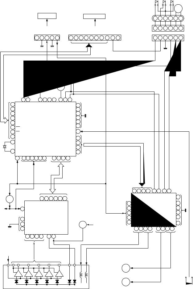
CD-BP2000W/210W/2000A/BK2000W/210W
XL1
16.93MHz
TO MAIN SECTION |
TO DISPLAY SECTION |
(TO IC601) |
R-CH |
AGND |
L-CH |
DGND |
+5V(+B5) |
CNP11 |
CDINT |
WRQ |
DRF |
CE |
DO |
DI |
CLK |
CD RES |
CLAMP SW |
GND |
CNP12 |
|
1 |
2 |
3 |
4 |
5 |
1 |
2 |
3 |
4 |
5 |
6 |
7 |
8 |
9 |
10 |
|||
|
|
|
|
|
|
|
|
|
|
|
|
Q2 |
|
|
|
|
|
75 |
76 |
|
|
45 |
46 |
47 |
48 |
32 |
31 |
30 |
|
65 |
CE |
CONT6 |
CONT7 |
|
|
LCHO |
LVSS |
RVSS |
RCHO |
CONT4 |
CONT3 |
CONT2 |
74 |
|
|
|
|
|
|
|
|
|
|
|
|
|
|
66 |
CL |
|
|
|
|
|
|
|
|
|
|
|
64 |
67 |
DI |
|
|
|
|
|
|
|
|
|
|
|
40 |
68 |
DO |
|
|
|
|
|
|
|
|
|
|
|
19 |
69 |
INT |
|
|
|
|
|
IC2 |
|
|
|
|
|
13 |
|
|
|
|
|
|
|
|
|
|
|
|||
|
|
|
|
|
|
|
|
|
|
|
|
3 |
|
70 |
WRQ |
|
|
|
|
LC78641E |
|
|
|
|
|||
|
|
|
|
|
|
|
|
|
|||||
|
|
|
|
|
SERVO/SIGNAL |
|
|
|
|
||||
71 |
RES |
|
|
|
|
CONTROL |
|
|
|
CONT5 |
33 |
||
72 |
DEF |
|
|
|
|
|
|
|
|
|
|
SLDO |
26 |
|
|
|
|
|
|
|
|
|
|
|
|
||
52 |
XOUT |
|
|
|
|
|
|
|
|
|
|
SPDO |
25 |
|
|
VVDD |
ADAVDD |
VDD |
LVDD |
RVDD |
XVDD |
|
HFL |
RFENV |
FE |
FDO |
24 |
51 |
VDD5V |
|
TE |
|
|||||||||
XIN |
|
|
|
|
|
|
|
|
|
|
TDO |
23 |
|
|
73 |
5 |
18 |
36 |
44 |
49 |
50 |
|
7 |
14 |
15 |
16 |
|
SW1 |
|
SW2 |
SW3 |
|
|
|
OPEN/ |
CLAMP |
DISC |
|
|
|
|
CLOSE |
|
|
NUMBER |
|
|
|
|
|
|
|
|
M |
M3 |
|
|
|
|
|
T/T |
|
|
|
|
|
|
UP/DOWN |
|
|
|
|
|
|
|
MOTOR |
|
|
|
+ |
|
- |
|
1 |
2 |
3 |
4 |
5 |
6 |
BI4 |
1 |
2 |
3 |
4 |
5 |
6 |
CNS4 |
|
||||||
1 |
2 |
3 |
4 |
5 |
6 |
CNP4 |
|
||||||
+5V |
+3.3V |
1 2 17 25 41 42 38 39
CONSTANT Q1
VOLTAGE
+3.3V |
30 |
23
11
9
+5V
PICKUP UNIT
|
|
|
17 |
18 |
19 |
20 |
21 |
22 |
|
|
|
|
|
|
|
|
|
35 |
|
|
|
|
|
|
|
|
|
|
|
|
|
||||||
|
|
|
HFL |
TE |
TE- |
FE |
FE- |
RFEV |
|
18 |
VCC1 |
|
|
|
IC3 |
|
|
29 |
|
|
|
|
|
|
|
|
|
|
|
|
|
|
|
||||
|
|
|
|
|
|
|
|
|
|
|
|
|
|
|
|
|
22 |
|
|
|
|
|
|
|
|
|
|
|
40 |
VCC4 |
|
|
M63001FP |
|
|
||
|
|
|
|
|
|
|
|
|
|
|
|
|
FOCUS/TRACKING/ |
|
21 |
|||
|
|
|
|
IC1 |
|
|
|
|
|
24 |
VCC2 |
|
SPIN/SLED DRIVER |
|
||||
|
|
|
|
|
|
|
|
|
+5V |
|
|
|
|
|
|
|
|
|
|
|
|
LA9235M |
|
|
|
|
|
|
|
|
|
|
|
14 |
|||
|
|
|
|
|
LASER |
|
23 |
|
|
|
|
|
|
|
||||
|
|
|
SERVO AMP. |
|
|
DRIVER |
|
|
|
|
|
|
|
|
|
|
||
|
|
|
|
|
|
|
|
Q3 |
+3.3V |
28 |
VCC3 |
|
|
|
|
|
|
8 |
|
|
|
|
|
|
|
|
|
|
|
|
|
|
|
|
|||
|
|
|
|
|
|
|
|
|
|
|
|
|
|
|
|
|
|
|
FIN1 |
FIN2 |
TIN1 |
TIN2 |
|
|
LDD |
|
|
|
|
4 |
5 |
6 |
7 |
15 |
16 |
26 |
27 |
|
PD |
|
|
|
|
|
|
|
|
|
|
|
|
|||||
1 |
2 |
3 |
4 |
|
7 |
8 |
|
|
|
|
|
|
|
|
|
|
|
|
|
|
M1 |
M |
|
|
SPINDLE |
|
|
|
MOTOR |
|
COIL |
COIL |
|
|
FOCUS |
TRACKING |
M2 |
M |
|
|
SLED |
|
|
|
MOTOR |
|
SW4
PICKUP IN
Figure 18 BLOCK DIAGRAM (1/4)
– 18 –
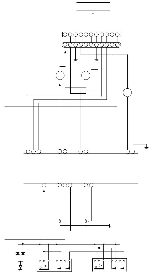
|
|
|
|
|
|
|
|
|
|
|
|
|
CD-BP2000W/210W/2000A/BK2000W/210W |
|||||
CD-BK2000W/BK210W ONLY |
|
|
|
TO MAIN SECTION |
|
|
|
|
||||||||||
|
|
|
|
|
|
|
|
|
|
(TO IC601) |
|
|
|
|
|
|||
|
|
|
|
|
|
OUT(L) |
IN(L) |
GND(A) |
+10V(A) |
OUT(R) |
IN(R) |
GND(D) |
DATA |
CLOCK |
LATCH |
MIC IN |
|
|
|
|
|
|
|
|
1 |
2 |
3 |
4 |
5 |
6 |
7 |
8 |
9 |
10 |
11 |
CNSK1 |
|
|
|
|
|
|
|
1 |
2 |
3 |
4 |
5 |
6 |
7 |
8 |
9 |
10 |
11 |
BIK1 |
|
|
|
|
|
|
QK3 |
|
|
|
QK2 |
|
|
|
|
|
|
|
|
|
|
|
|
|
|
|
|
|
|
|
|
|
|
|
|
|
|
QK1 |
|
|
42 |
41 |
40 |
|
36 |
35 |
|
|
32 |
31 |
|
|
|
|
|
|
23 |
22 |
ICK1 M65856SP MIC AMP. |
DATA |
CLDCK |
LATCH |
|
MICLOUT LOUT |
ROUT |
|
|
RIN |
LIN |
|
|
|
|
|
|
VCC |
GND |
MIC1IN |
MIC1VOLIN |
MIC2IN |
|
MIC2OUT |
MIC2VOLIN |
|
|
|
|
|
||||||||
|
|
|
|
4 |
7 |
8 |
9 |
|
|
12 |
13 |
|
|
|
|
|
|
|
|
|
|
|
|
|
|
|
|
|
|
|
VRK1 |
|
|
|
|
|
|
|
|
|
|
|
VRK2 |
|
|
|
|
|
|
MIC1 |
|
|
|
|
|
|
|
|
|
|
|
MIC2 |
|
|
|
|
|
|
VOLUME |
|
|
|
|
||
|
|
|
|
VOLUME |
|
|
|
|
|
|
|
|
|
|
|
|
|
|
PINK1 |
|
|
|
|
|
|
|
|
|
|
|
|
|
|
|
|
|
|
CHASIS |
|
|
|
JK2 |
|
|
|
|
|
|
|
|
JK1 |
|
|
|
||
GND |
|
|
|
|
MIC2 |
|
|
|
|
|
|
|
|
MIC1 |
|
|
|
|
Figure 19 BLOCK DIAGRAM (2/4)
– 19 –
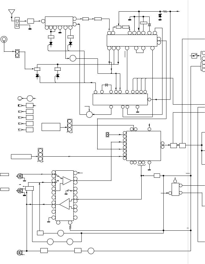
CD-BP2000W/210W/2000A/BK2000W/210W
|
FM |
|
|
|
|
|
|
|
|
|
|
|
|
|
|
|
|
|
|
|
|
|
|
|
|
|
|
|
|
|
|
ANTENNA |
|
|
|
|
|
|
|
|
|
|
|
|
|
|
|
|
|
|
|
|
|
|
|
|
|
|
+5V |
|
|
||
|
|
|
|
|
|
|
|
|
|
|
|
|
|
|
|
|
|
|
|
|
|
|
|
|
|
|
|
+B4 |
|
||
|
|
|
|
|
|
|
|
|
|
|
|
|
|
|
|
|
|
|
|
|
|
|
|
|
|
|
|
|
|
|
|
|
SO302 |
|
|
|
|
|
|
|
|
|
FM IF |
|
|
|
|
|
|
|
|
|
|
|
|
|
|
|
|
|
|
|
|
|
|
|
|
|
|
|
|
|
|
6 |
|
|
|
|
|
|
|
|
|
|
|
|
|
|
|
|
|
|
|
|
|
|
|
|
BF301 |
|
1 |
|
|
IC301 |
|
|
T302 |
CF303 |
|
|
|
|
|
|
|
|
|
|
|
|
|
|
|
|
|
||
|
|
|
|
|
TA7358AP |
|
|
|
|
|
|
|
|
|
|
|
|
|
|
|
|
|
|
|
|
|
|
||||
|
|
|
B.P.F |
|
|
|
|
|
|
|
|
|
|
|
|
|
|
|
CF351 |
|
|
|
|
|
|
|
|||||
|
|
|
|
|
|
FM FRONT END |
9 |
|
|
|
|
|
|
|
|
|
|
|
|
|
X351 |
|
|
|
|
|
|||||
|
|
|
|
|
2 |
3 |
4 |
5 |
7 |
8 |
|
|
|
|
|
|
T351 |
CF352 |
|
|
|
|
|
|
456kHz |
|
|
|
|
|
|
|
|
|
|
|
|
|
|
|
|
|
|
|
|
|
|
|
|
|
|
|
|
|
|||||||||
|
|
|
|
|
|
|
|
|
FM OSC |
|
|
|
|
|
|
AM IF |
|
|
|
|
|
|
|
|
|
|
|
|
|
||
AM LOOP |
|
|
|
|
|
|
|
|
|
|
|
1 |
|
2 |
|
|
|
4 |
5 |
9 |
8 |
17 |
13 |
|
|
|
|
|
|||
ANTENNA |
|
|
|
|
|
|
|
|
|
|
|
|
|
|
AM MIX |
|
AM IF GND VCC FM |
VCO MO/ST |
|
|
|
|
|
||||||||
|
|
|
|
|
FM RF |
L312 |
|
|
T301 |
|
|
|
|
|
|
|
|
|
|
||||||||||||
|
|
|
|
|
|
|
|
|
|
|
|
|
IC303 |
|
|
|
|
DET |
|
L 14 |
|
|
|
|
|
||||||
|
|
|
|
|
|
|
|
|
|
FM OSC |
|
|
|
|
|
LA1832S |
|
|
|
|
|
|
|
|
|
|
|||||
|
|
|
|
|
|
|
|
|
|
|
|
|
|
|
|
|
|
|
|
|
|
|
|
|
|
|
|||||
|
|
|
|
|
|
|
|
|
|
|
|
|
|
FM IF DET./FM MPX./AM IF |
|
|
|
|
R 15 |
|
|
|
|
|
|||||||
|
|
|
|
|
|
|
|
|
|
|
|
|
|
|
|
|
|
|
|
|
FM/AM |
|
|
|
|
|
|
|
|||
|
|
|
|
|
|
|
|
|
|
|
|
|
|
|
|
|
|
|
|
|
|
OUT |
MPXIN |
FM/AM |
|
|
|
|
|
||
|
|
2 |
|
|
|
|
|
|
|
|
|
|
|
24 |
23 |
21 |
|
7 |
|
|
18 |
|
16 |
|
12 |
|
|
|
+B4 |
~ |
|
|
|
|
|
|
|
|
|
|
|
|
|
|
OSCOUT |
OSCIN |
INRF |
STEREO |
|
|
|
|
|
|
|
|
|
|
|||||
|
|
1 |
|
|
|
|
|
|
|
OSC BUFF |
|
|
|
|
|
|
|
|
|
|
|
|
|
|
|
|
|
|
|
|
5 |
|
|
|
|
|
|
|
|
|
|
|
|
|
|
|
|
|
|
|
|
|
|
|
|
|
|
|
|
|
|
||
|
|
|
|
|
|
|
|
|
|
|
|
|
|
|
|
|
|
|
|
|
|
|
|
|
|
|
|
|
|
|
|
|
|
|
|
|
|
|
|
|
|
Q302 |
|
FM OSC |
|
AM |
AM |
AM |
|
|
|
|
|
|
|
|
|
|
|
|
|
8 |
|
|
|
|
|
|
|
|
|
|
|
|
|
|
|
|
|
|
|
|
|
|
|
|
|
|
|
||||||
|
|
|
|
|
|
|
|
|
|
|
|
|
|
|
|
|
|
|
|
|
|
|
|
|
|
|
|
||||
|
|
|
AM |
|
|
|
|
|
|
|
|
|
|
|
|
|
|
|
|
|
|
|
|
|
|
|
|
|
|
|
12 |
|
|
|
|
|
|
|
|
|
|
|
|
|
|
|
|
|
|
|
|
|
|
|
|
|
|
|
|
|
|
13 |
|
|
|
|
TRACKING |
|
|
|
|
AM BAND |
|
|
|
|
|
|
|
|
|
|
|
|
|
|
|
|
|
|
|
|
|||
|
|
|
|
T303 |
|
|
T306 |
|
|
|
|
|
|
|
|
|
|
|
|
|
|
|
|
|
|
|
|
14 |
|||
|
|
|
|
|
|
COVERAGE |
|
|
|
|
|
|
|
|
|
|
|
|
|
|
|
|
|
|
|
|
|||||
|
|
|
|
|
|
|
|
|
|
|
|
|
|
X352 |
|
|
|
|
|
|
|
|
|
|
|
|
|
|
|
|
IN |
|
|
|
|
|
|
|
|
|
|
|
|
VT |
|
|
IN |
IN |
|
|
|
|
|
|
|
|
|
|
|
|
|
E |
|
|
|
|
|
|
|
|
|
|
|
|
|
|
4.5MHZ |
|
|
|
|
|
|
|
|
|
|
|
|
|
|
||||
|
|
|
|
|
|
|
|
|
|
|
|
|
|
AM |
FM |
|
|
|
|
|
|
|
|
|
|
|
|
|
|
||
|
|
|
|
|
|
|
|
|
|
|
|
|
|
|
|
|
|
|
|
|
|
DO |
|
|
|
|
|
|
|
||
|
|
|
|
|
|
|
|
|
|
|
|
|
|
|
|
|
|
|
|
CE |
|
DI |
CL |
|
|
|
|
|
|
|
|
|
|
|
MOTOR |
|
|
|
|
|
|
|
|
20 |
1 |
22 |
15 16 |
11 |
3 |
4 |
5 |
6 |
|
|
|
|
|
|
|
||||
|
MM1 |
|
DRIVER |
|
|
|
|
|
|
|
|
|
|
OSC |
|
IC302 |
|
|
|
|
|
|
|
|
|
|
|
|
|
|
|
|
M |
Q708 |
+3B |
|
|
|
|
|
|
|
|
|
|
|
|
|
|
|
|
|
|
|
|
|
|
|
|
||||
|
TAPE |
|
|
|
|
|
|
|
|
|
|
LC72131 |
|
|
|
|
|
VDD |
17 |
|
|
|
|
|
|
||||||
MOTOR |
|
|
|
|
|
|
|
|
|
|
|
|
|
|
|
|
|
|
|
|
|
|
|
|
|
||||||
|
|
|
|
|
|
|
|
|
|
|
|
|
|
|
PLL(TUNER) |
|
|
|
|
|
|
|
|
|
|
|
|
|
|||
SOLM1,SOLM2 |
Q704 |
+3B |
|
|
|
|
|
|
|
|
|
|
|
FM/AM |
MO/ST |
|
|
|
|
|
|
|
|
|
|
|
|||||
|
|
|
|
|
+B4 |
|
|
7 |
|
|
9 |
10 |
|
|
|
|
|
|
|
|
|
|
|
|
|||||||
SOLENOID |
|
Q705 |
|
|
|
|
|
|
|
|
|
|
|
|
|
21 |
|
|
|
|
|
|
|
|
|||||||
SWM2 |
|
IC701 |
|
|
|
|
|
|
|
|
|
|
|
|
|
|
|
|
|
|
|
|
|
|
|
|
|
|
|
|
|
T2 PLAY |
|
54PIN |
|
|
|
|
|
|
|
FM +B |
|
FM |
|
|
|
|
|
|
|
|
|
|
|
|
|
|
|
|
|
||
SWM1 |
|
IC701 |
|
|
|
|
|
|
|
|
Q360 |
|
|
|
|
|
|
|
|
|
|
|
|
|
|
|
|
|
|
|
|
|
|
|
|
|
|
|
CNP601 |
|
|
|
|
|
|
|
|
|
|
|
|
|
|
|
|
|
|
|
|
|
|||
T1 PLAY |
|
53PIN |
|
|
|
|
|
|
|
SWITCHING |
|
|
|
|
|
|
|
|
|
|
|
|
|
|
|
|
|
|
|
||
|
|
|
|
|
|
|
1 |
|
|
|
|
|
|
|
|
|
|
|
|
|
|
|
|
|
|
|
|
||||
SWM4 |
|
IC701 |
|
|
|
|
|
|
|
|
|
|
|
|
|
|
|
|
|
|
|
|
+B4 |
|
|
|
|
|
|||
|
|
|
|
|
|
|
|
|
|
|
|
|
|
|
|
|
|
|
|
|
|
|
|
|
|
|
|
|
|||
R. PLAY |
|
56PIN |
|
FROM KARAOKE |
|
2 |
|
|
|
|
|
|
|
|
|
|
|
|
|
|
|
|
|
|
|
|
|
||||
SWM3 |
|
IC701 |
|
SECTION |
|
|
|
|
|
|
|
|
|
|
|
|
7 |
|
18 |
|
|
23 |
|
|
|
|
|
|
|||
|
|
|
CNSK1 |
|
|
3 |
|
|
|
JK601 |
|
|
|
|
|
|
|
|
|
|
|
|
|
|
|||||||
F. PLAY |
|
55PIN |
|
|
|
|
|
|
|
|
|
|
VIDEO IN |
|
|
L 9 |
|
L |
|
R |
|
|
|
|
|
|
|
|
|
||
|
|
|
|
|
|
|
|
|
|
|
|
|
|
L |
|
AUX |
|
|
|
|
|
|
|
|
|
|
|
||||
|
|
|
|
|
|
|
|
|
|
|
|
|
|
R |
|
|
|
R 16 |
|
|
|
|
|
|
|
|
|
|
|
|
|
|
|
|
|
|
|
|
|
|
|
|
|
|
|
|
|
TAPE |
L 10 |
|
|
|
|
|
|
|
|
|
-20dB |
SYSTEM |
|
||
|
|
|
|
|
|
|
|
|
|
|
|
|
|
|
|
|
|
R 15 |
|
|
|
|
IC601 |
|
21 |
R |
|
ATT |
MUTE |
|
|
|
|
|
|
|
|
|
|
|
|
|
|
|
|
|
|
|
|
|
|
|
|
|
|
Q603 |
Q605 |
|
|||||
|
|
|
|
CNS601 |
|
|
|
|
|
|
|
|
|
TUNER |
L 11 |
|
|
|
LC75341 |
4 |
L |
|
Q604 |
Q606 |
L |
||||||
|
|
|
|
|
1 |
|
|
|
|
|
|
|
|
|
|
|
|
R 14 |
AUDIO PROCESSOR |
|
|
|
|
||||||||
|
|
|
|
|
|
|
|
|
|
|
|
|
|
|
|
|
|
|
|
|
|
||||||||||
|
|
|
|
|
|
|
|
|
|
|
|
|
|
|
|
|
|
|
|
|
|
|
|
|
|
|
|
|
|||
|
FROM CD SECTION |
|
2 |
|
|
|
|
|
|
|
|
|
|
|
CD |
L 12 |
|
|
|
|
|
|
|
|
|
|
|
|
|
||
|
|
CNP11 |
|
|
3 |
|
|
|
|
|
|
|
|
|
|
|
|
R 13 |
|
|
L |
R |
|
|
|
|
|
|
|
||
|
|
|
|
|
|
|
|
|
|
|
|
|
|
|
|
|
|
|
|
|
|
|
|
|
|
||||||
|
|
|
|
|
|
|
|
|
IC101 |
|
|
|
|
|
|
|
|
|
7 |
|
8 |
17 18 |
3 |
|
|
|
|
|
R |
||
|
|
|
|
|
|
|
|
AN7345K |
|
|
|
|
|
|
|
|
|
|
|
|
|
|
|
|
|
|
|
|
|
||
|
|
|
|
|
|
PLAYBACK AND RECORD |
|
|
|
|
|
|
|
|
|
|
|
|
|
|
|
|
|
+B4 |
|
|
|||||
|
|
|
|
|
|
|
|
/PLAYBACK AMP. |
|
|
|
|
|
|
|
|
|
|
|
|
|
|
|
|
|
|
|
|
|||
TAPE 1 |
L-CH |
|
|
|
L(T1) |
1 |
|
|
VCC 13 |
|
+B4 |
|
|
|
|
|
|
|
|
|
|
|
|
|
Q121 |
|
|
|
REC |
|
|
|
|
|
R(T1) |
24 |
|
|
|
|
|
|
|
|
|
|
|
|
|
|
|
|
|
|
|
|
|
|
|||||
PB HEAD |
R-CH |
|
|
|
|
P.B |
|
|
|
|
|
|
|
|
|
|
|
|
|
|
|
Q122 |
|
|
|
|
|
||||
|
|
|
|
|
|
|
|
4 |
L |
|
|
|
|
|
|
|
|
|
|
|
|
|
|
MUTING |
|
|
|
|
|
||
|
|
|
|
|
L(T2) |
2 |
|
|
P.B |
|
|
|
|
|
|
|
|
|
|
|
|
|
|
|
8 |
|
|
||||
|
|
|
|
|
|
|
21 |
R |
|
|
|
|
|
|
|
|
|
|
|
|
|
|
|
|
|
|
|
||||
|
|
REC |
|
|
R(T2) |
23 |
|
|
|
|
|
|
|
|
|
|
|
|
|
|
|
|
|
|
|
|
|
|
|||
|
|
SWITCHING |
|
|
|
|
|
|
|
|
|
|
|
|
|
|
|
|
|
|
|
|
|
|
1 |
|
|||||
|
|
P.B |
Q103- |
|
L NF |
3 |
|
|
5 |
|
|
|
|
|
|
|
|
|
|
|
|
|
|
|
|
|
|
IC561 |
|
||
TAPE 2 |
L-CH |
|
Q106 |
|
|
|
|
|
|
|
|
|
|
|
|
|
|
|
|
|
|
|
|
|
IC562 |
|
|
||||
REC PB HEAD R-CH |
|
|
|
R NF |
4 |
|
|
20 |
|
|
|
|
|
|
|
|
|
|
|
|
|
|
|
-B2 |
|
4 |
IC563 |
7 |
|
||
|
|
|
|
|
|
|
|
|
|
|
|
|
|
|
|
|
|
|
|
|
|
|
|
||||||||
|
|
|
|
|
|
|
6 |
|
|
H/N |
|
|
|
|
|
|
|
|
|
|
|
|
|
|
|
|
|
|
OPE |
|
|
|
|
AC BIAS |
|
|
POP REDUCE |
T1/T2 |
|
7 |
L |
REC |
|
|
|
|
|
|
|
|
|
|
|
|
|
|
|
|
|
|
|||
|
|
|
|
|
|
|
|
|
|
18 |
R |
|
|
|
|
|
|
|
|
|
|
|
|
|
|
|
|
|
AMP. |
|
|
|
|
|
|
|
L REC |
9 |
REC |
|
|
|
|
|
|
|
|
|
|
|
|
|
|
|
|
|
KIA4558P |
|
|
||||
|
|
|
|
|
|
|
|
|
|
|
|
|
|
|
|
|
|
|
|
|
|
|
|
|
|
||||||
|
|
|
|
|
R REC 16 |
|
|
8 |
L NF |
|
|
|
|
|
|
|
|
|
|
|
|
|
|
|
|
|
|
|
|
||
|
|
|
|
|
REF 14 |
|
|
17 R NF |
|
|
|
|
|
|
|
|
|
|
|
|
|
|
|
|
|
|
|
|
|||
|
|
|
|
|
|
|
|
|
|
|
|
|
|
|
|
|
|
|
|
|
|
|
|
|
|
|
|
|
|||
|
|
12 NOR/ |
|
10 ALC |
|
|
|
|
HIGH |
T1/T2 |
|
|
|
|
|
15 |
|
19 |
|
|
|
|
SWITCHING |
|
|
T1/T2 |
|
|
Q107 |
Q111 |
|
|
|
|
|
Q108 |
|
|
|
|
|
|
|
|
|
|
|
|
|
SWITCHING |
|
|
|
|
|
|
|
Q109 SWITCHING Q110 |
|
|
||
|
|
|
|
|
BIAS |
|
|
Q128 |
|
|
Q124 |
Q126 |
BIAS |
ERASE |
BIAS L104 |
|
|
L103 |
|
|
HEAD |
OSC |
|
|
SWITCHING |
|
|
Figure 20 BLOCK DIAGRAM (3/4)
– 20 –
|
|
|
|
|
|
|
|
|
|
|
|
|
|
|
|
CD-BP2000W/210W/2000A/BK2000W/210W |
|||||||||||||||
+B4 |
|
|
|
|
|
|
|
|
|
|
|
|
|
|
FL701 |
|
|
|
|
|
|
|
|
|
|
|
|
|
|
|
|
|
|
|
|
|
|
|
|
|
|
|
|
|
|
DISPLAY |
|
|
|
|
|
|
|
|
|
|
|
|
|
|
|
||
|
|
|
|
|
|
|
|
|
|
|
|
|
|
|
|
|
|
|
|
|
|
|
|
|
|
|
|
|
|
||
|
|
|
SW601 |
|
|
|
|
1 |
2 |
3 |
|
6 ~ 14 |
15 ~ 20 |
29 ~ 53 |
56 |
57 58 |
|
|
|
|
|
|
|
|
|
|
|||||
|
|
|
|
|
|
|
|
|
|
|
|
|
|
|
|
|
|
|
|
|
|
|
|
|
|
|
|
|
|
||
|
|
|
SPAN |
|
|
|
|
|
|
|
|
|
|
|
|
|
|
|
|
|
|
|
|
|
|
|
|
|
|
|
|
|
|
|
SELECTOR |
|
|
|
|
|
|
|
|
|
|
|
|
|
|
|
|
|
|
|
|
|
|
|
|
|
|
||
|
|
|
|
|
|
|
Q701-Q703 |
|
|
|
|
|
|
|
|
|
|
|
|
|
|
|
|
|
|
|
|
|
|
|
|
|
|
|
|
|
|
|
Q710-Q712 |
|
|
|
|
|
|
|
|
|
|
|
|
+B7 |
|
|
|
|
|
JOG701 |
|
|
|||
|
|
|
|
|
|
|
|
|
|
|
|
|
|
|
|
|
|
|
|
|
|
|
|
|
|
|
|
||||
|
|
|
|
|
|
|
|
|
|
|
|
|
|
|
|
|
|
|
|
|
|
|
|
|
|
|
|
JOG |
|
|
|
|
|
+B6 |
|
|
|
|
|
|
|
|
|
|
|
|
|
|
|
|
|
|
|
|
|
|
|
|
|
|
|
RX701 |
|
|
|
|
|
|
|
|
|
|
|
|
|
|
|
|
|
|
|
|
|
|
|
|
|
|
|
|
|
|
|
REMOTE |
|
|
|
18 |
|
|
|
|
|
|
|
|
27 |
|
|
|
52 |
51 |
50 49 |
48 |
47 46 |
45 |
44 |
43 |
42 |
41 |
40 |
|
|
SENSOR |
|
||
|
|
|
|
|
|
|
|
|
|
|
|
|
|
|
|
|
|
|
|
VDD |
|
|
|
|
|
|
39 |
|
1 |
3 |
|
|
5 |
|
1 |
|
|
|
|
|
|
|
|
|
|
|
|
|
|
|
|
|
|
|
|
|
|
|
|
||||
|
|
|
|
|
|
|
|
|
|
|
|
|
|
|
|
|
|
|
|
|
|
|
|
|
|
|
|
+B7 |
|||
|
|
|
|
|
|
|
|
|
|
|
|
|
|
|
|
|
|
|
|
|
|
|
|
|
|
38 |
|
2 |
|||
+B4 |
~ |
|
2 |
|
|
|
|
|
|
|
|
|
|
|
|
|
|
|
|
|
|
|
|
|
|
|
|
|
|||
DI |
|
|
|
|
|
|
|
|
|
|
|
|
|
|
|
|
|
|
|
|
|
|
|
|
37 |
|
|
|
|||
8 |
|
|
|
|
|
|
|
|
|
|
|
|
|
|
|
|
|
|
|
|
|
|
|
|
|
|
|
||||
|
|
|
|
|
|
|
|
|
|
|
|
|
|
|
|
|
|
|
|
|
|
|
|
|
|
|
|
||||
|
CL |
3 |
|
|
|
|
|
|
79 VLOAD |
|
|
|
|
|
|
|
|
|
|
|
|
|
|
|
|
|
|
||||
|
12 |
|
|
|
|
|
|
|
|
|
|
|
|
|
|
|
|
|
|
SYS. STOP |
36 |
|
|
|
|||||||
|
|
4 |
|
|
|
|
|
|
80 |
|
|
|
|
|
|
|
|
|
|
|
|
|
|
|
|
|
|||||
|
LCK |
|
|
|
|
|
|
|
|
|
|
|
|
|
|
|
|
|
|
|
|
|
|
|
35 |
|
|
|
|||
|
13 |
|
|
|
|
|
|
|
|
|
|
|
|
|
|
|
|
|
|
|
|
|
|
|
|
|
|
||||
|
|
|
|
|
|
|
|
|
~ |
|
|
|
|
|
|
|
IC701 |
|
|
|
|
|
|
|
|
|
|
|
|||
|
|
|
|
|
|
|
|
|
|
|
|
|
|
|
|
|
|
|
|
|
|
|
|
|
+B7 |
|
|
||||
|
|
|
|
|
|
|
|
|
85 |
|
|
|
|
|
|
|
|
|
|
|
|
|
AVDD |
34 |
|
|
|||||
|
14 |
|
|
|
|
|
|
|
|
|
|
|
|
|
|
IX0334AW |
|
|
|
|
|
|
KEY |
|
|||||||
|
|
|
|
|
|
|
|
|
|
|
|
|
|
|
|
|
|
|
|
|
|
|
33 |
|
|
||||||
|
|
IC702 |
|
|
|
|
|
|
|
86 |
|
|
|
|
|
|
SYSTEM |
|
|
|
|
|
|
|
|
|
SW701-SW703 |
||||
|
|
|
|
|
|
|
|
|
~ |
|
|
|
|
|
MICROCOMPUTER |
|
|
|
|
|
|
~ |
|
SW709-SW716 |
|||||||
|
|
BU2092F |
|
|
|
|
|
|
|
91 |
|
|
|
|
|
|
|
|
|
|
|
31 |
|
SW722-SW735 |
|||||||
|
INPUT/OUTPUT |
|
|
|
|
|
|
|
|
|
|
|
|
|
|
|
|
|
|
|
|
|
|
|
|
|
|
||||
|
EXPANDER |
|
|
|
|
|
|
92 |
|
|
|
|
|
|
|
|
|
|
|
|
|
|
|
|
|
|
|
|
|
||
|
|
|
|
|
|
|
|
|
|
|
|
|
|
|
RESET |
|
|
|
|
|
|
|
|
|
|
|
|
|
|
|
|
|
|
|
|
|
|
|
|
|
|
~ |
VDD |
|
|
|
|
|
|
|
VDD |
|
|
|
|
|
|
|
|
+B3 |
|
||
|
|
|
|
|
|
|
|
|
100 |
|
|
|
|
|
|
|
|
|
CE |
CL |
DI |
DO |
25 |
|
|
||||||
|
|
|
|
|
|
|
|
|
|
|
|
|
|
|
|
|
|
|
|
|
|||||||||||
|
|
|
|
|
|
|
|
|
|
|
1 |
2 |
3 |
5 |
7 ~ 9 10 11 12 13 15 16 17 ~ 20 21 24 |
23 24 |
|
|
JK670 |
||||||||||||
|
|
|
|
|
|
|
|
|
|
|
|
|
|
|
|
|
|
|
|
|
|
|
|
|
|
|
|
|
|
||
|
|
|
|
|
|
|
|
|
|
|
|
|
|
|
|
|
|
|
|
|
|
|
|
|
|
|
|
|
|
HEADPHONES |
|
|
|
|
|
|
|
|
|
|
|
|
+B7 |
|
|
|
|
|
XL701 |
|
+B7 |
|
|
|
|
|
|
|
|
TO CD |
|||
|
|
|
|
|
|
|
|
|
|
|
|
|
|
|
|
|
|
|
|
|
|
|
|
|
|
|
|
SECTION |
|||
|
|
|
|
|
|
|
|
|
|
|
|
|
|
|
|
|
4.1943MHz |
|
|
|
|
|
|
|
|
|
|
|
+B5 |
||
|
|
|
|
|
|
|
|
|
|
|
|
|
|
|
|
|
|
|
|
|
|
|
|
|
|
|
|
|
|
|
|
|
|
|
|
|
|
|
|
|
|
|
|
|
|
|
|
|
|
|
|
|
|
|
|
|
|
|
|
|
DRIVER |
|
|
|
|
|
|
|
|
|
|
|
|
|
|
|
|
RESET |
Q709 |
|
|
|
IC703 |
|
|
|
|
|
|
|
Q910 |
M |
|||
|
|
|
|
|
|
|
|
|
|
|
|
|
|
|
|
|
3 KIA7042AP |
1 |
|
|
|
|
|
||||||||
|
|
|
|
|
|
|
|
|
|
|
|
|
|
|
|
|
|
|
|
|
|
|
|
|
|
||||||
|
|
|
|
|
|
|
|
|
|
|
|
|
|
|
|
|
|
|
|
|
RESET |
|
|
+B7 |
|
|
|
M901 |
|||
|
|
|
|
|
|
|
|
|
|
|
|
|
Q905 |
|
|
|
|
|
|
|
2 |
|
|
|
|
|
|||||
|
|
|
|
|
|
SP. DET. |
|
|
|
|
|
|
|
|
|
|
|
|
|
|
|
|
FAN MOTOR |
||||||||
|
|
|
|
|
|
|
|
|
|
Q906 |
|
|
|
|
|
|
|
|
|
|
|
|
|
|
|||||||
|
|
|
|
|
|
|
|
|
|
|
|
|
Q907 |
|
|
|
|
|
|
|
|
|
|
|
|
|
|
|
|
|
|
|
|
|
|
|
|
|
|
|
|
|
|
|
Q908 |
|
|
|
|
|
|
|
|
|
|
|
|
|
|
RL901 |
|
|
|
|
|
|
|
|
|
|
|
|
|
|
|
|
|
|
|
|
|
|
|
|
|
|
|
|
|
Q909 |
|
|
|
||
|
|
|
|
|
|
|
|
|
|
|
|
|
R |
|
|
|
|
|
|
|
|
|
|
|
|
|
|
|
|
||
|
|
|
|
|
|
|
|
|
|
|
|
|
IC902 |
|
|
|
|
|
|
|
|
|
|
|
|
|
|
MAIN |
|||
|
|
|
|
|
|
|
|
|
|
|
|
|
|
1 |
|
|
7 R-OUT |
|
|
|
|
|
|
|
|
|
|||||
|
|
|
|
|
|
|
|
|
|
|
|
|
|
STK402-040 |
|
|
|
|
|
|
|
|
|
|
SUB |
||||||
|
|
|
|
|
|
|
|
|
|
|
|
|
|
15 |
POWER AMP. |
|
10 L-OUT |
|
|
|
|
|
|
|
|
|
|||||
|
|
|
+B4 |
|
|
|
|
|
|
|
|
|
L |
-Vcc |
|
13 |
|
|
|
|
|
|
|
|
|
|
|
WOOFER |
|||
|
|
|
|
|
|
|
|
|
|
|
|
|
|
+Vcc |
9 |
|
|
|
|
|
|
|
|
|
|
|
|
|
|
SO901 |
|
SYSTEM |
|
|
|
|
|
|
|
|
|
|
|
|
|
|
|
|
|
|
|
|
|
|
|
|
|
|
|
|
|||
|
|
|
|
|
|
|
|
Q901 |
|
|
|
|
|
8 |
|
|
|
|
|
|
|
|
|
|
|
|
RL902 |
SPEAKER |
|||
MUTE |
|
|
8 |
|
|
|
|
|
Q902 |
|
|
|
|
|
|
|
|
|
-B2 |
|
|
|
|
|
|
|
|
TERMINAL |
|||
Q605 |
|
|
|
|
|
|
|
Q903 |
|
|
|
|
|
|
|
|
|
|
|
|
|
|
|
|
|
|
|
|
|||
|
|
|
|
|
|
|
|
|
|
|
|
|
|
|
|
|
|
|
|
|
|
|
|
|
|
|
|
|
|||
Q606 |
L |
5 |
|
|
|
|
|
|
Q904 |
|
|
|
|
|
|
|
|
|
|
|
|
|
|
|
|
|
|
|
|
|
|
|
|
|
|
|
|
|
|
|
|
|
|
|
|
|
|
|
|
|
F802 |
|
|
|
T801 |
|
|
|
|
||||
|
|
6 |
|
|
|
|
|
|
|
|
|
|
|
|
|
|
|
|
|
|
T5A L 250V |
POWER TRANSFORMER |
|
|
|||||||
|
|
|
|
|
|
IC901 |
|
|
|
|
|
|
|
|
|
|
|
|
|
|
|
|
|
|
|
|
|||||
|
|
IC903 KIA4558P OPEAMP. |
7 |
L |
R 1 |
|
7 R-OUT |
|
|
D802 |
|
|
|
|
|
|
|
|
|
|
|
|
|
|
|||||||
|
|
STK402-071 |
|
|
|
|
|
|
|
|
|
|
|
|
|
|
|
|
|
||||||||||||
|
|
|
|
+B2 |
|
|
|
|
|
|
|
|
|
|
|
|
|
|
|
|
|||||||||||
|
|
1 |
R |
L 15 POWER AMP. |
10 L-OUT |
|
|
|
|
|
|
F800 |
|
|
|
|
|
|
|
|
|
||||||||||
|
|
|
|
|
|
|
|
|
|
|
|
|
|
|
|
|
|
||||||||||||||
|
|
|
|
|
|
-Vcc |
13 |
|
|
|
|
|
|
|
|
|
|
|
T4A L 250V |
|
|
|
|
|
230–240V |
SW801 |
|||||
|
R |
2 |
|
|
|
|
+Vcc |
9 |
|
|
|
|
|
|
|
|
|
|
|
|
|
|
|
|
|
|
|
|
VOLTAGE |
||
|
|
|
|
|
|
|
|
|
|
|
|
|
|
|
|
|
|
|
|
|
|
|
|
|
|
|
|||||
|
|
3 |
|
|
|
|
8 |
|
|
|
|
|
|
|
D803 |
|
|
|
|
|
|
|
|
|
|
|
|
|
SELECTOR |
||
|
|
|
4 |
|
|
|
+B1 |
|
|
|
|
|
|
|
|
|
|
|
|
|
|
|
|
|
|
|
|
|
|
|
|
|
|
|
|
|
|
|
|
|
|
|
|
|
|
|
|
|
|
|
|
|
|
|
|
|
|
|
|
220V |
|
||
REC |
|
|
|
|
|
|
|
-B1 |
|
|
|
|
|
|
|
|
|
|
|
|
|
|
|
|
|
|
|
|
|
|
|
|
|
-B2 |
|
|
|
|
|
|
|
|
|
|
|
|
|
|
|
|
F801 |
|
|
|
|
|
|
|
|
|
|||
|
|
|
|
|
|
|
|
|
|
|
|
|
|
|
|
|
|
|
|
|
|
|
|
|
|
|
|
||||
|
|
|
|
|
|
|
|
|
|
|
|
|
|
|
|
|
|
|
T4A L 250V |
|
|
|
|
|
|
|
|
|
|||
|
|
|
|
|
|
|
|
|
|
|
|
|
|
|
|
|
|
|
|
|
|
|
|
|
|
|
|
|
|
||
|
|
10Hz |
|
|
|
|
|
|
|
|
|
|
|
|
|
|
|
|
|
F803 |
|
|
|
|
|
|
|
127V |
|
||
1 |
|
|
|
|
|
|
|
|
|
|
|
|
|
|
|
|
|
|
|
|
|
|
|
|
|
|
|
|
|||
|
|
|
|
|
|
|
|
|
|
|
|
|
|
|
|
|
|
|
|
|
|
|
|
|
|
|
110V |
|
|||
|
|
|
27 |
|
|
|
|
|
|
|
|
|
|
|
|
|
|
|
|
|
T5A L 250V |
|
|
|
|
|
|
|
|||
|
|
|
|
|
|
|
|
|
|
|
|
|
|
|
|
|
|
|
|
|
|
|
|
|
|
|
|
|
|
|
|
7 |
|
|
IC701 |
|
|
|
|
|
|
|
|
CONSTANT |
|
D804-D807 |
|
|
|
|
|
|
|
|
|
|
|
RL801 |
|||||
|
|
IX0334AW |
|
|
|
|
|
|
|
VOLTAGE |
|
|
|
|
|
|
|
|
|
|
|
|
|
|
|
|
|
||||
|
|
SYSTEM |
|
|
|
|
M10V |
|
|
|
|
|
|
|
|
|
|
|
|
|
|
|
|
|
|
|
D801 |
|
|||
|
|
MICROCOMPUTER |
|
|
+B3 |
|
|
Q823 |
|
|
|
|
|
|
|
|
|
|
|
|
|
|
|
|
|
||||||
|
|
|
28 |
|
|
|
|
|
|
|
|
|
|
|
|
|
|
|
|
|
|
|
|
|
|
|
|
|
|
|
|
|
|
|
|
|
|
|
|
|
|
|
|
|
|
|
|
|
|
|
|
|
|
|
|
|
|
|
|
|
|
|
|
|
|
|
|
|
|
|
|
|
|
|
|
IC802 |
|
|
|
|
|
|
|
F805 |
|
|
|
|
|
|
|
|
|
||
|
|
|
|
|
|
|
|
|
A10V |
|
|
|
|
|
|
|
|
T2A L 250V |
|
|
|
|
|
|
|
|
|
||||
|
|
63Hz |
|
|
|
|
+B4 |
KIA7810AP |
|
|
|
|
Q801 |
|
|
|
|
|
|
|
|
|
|
||||||||
|
|
|
|
|
|
|
|
|
|
|
|
|
|
|
|
|
|
|
|
|
|
|
|
||||||||
|
|
|
|
|
|
|
|
|
|
|
|
VOLTAGE |
|
|
|
|
|
|
|
|
|
|
|
|
|
|
|
|
|
|
|
|
|
|
|
|
|
|
|
|
|
|
REGULATOR |
|
|
|
|
|
|
|
|
|
|
|
|
|
|
|
|
|
|||
|
|
|
|
|
|
|
VF2 |
|
|
|
|
|
|
|
|
|
|
|
|
|
|
|
|
|
|
|
|
|
|
|
AC POWER |
|
|
|
|
|
|
|
|
|
|
|
|
|
|
|
|
|
|
|
|
|
|
|
|
|
|
|
|
|
|
SUPPLY CORD |
|
|
|
|
|
|
|
|
|
|
|
VF1 |
|
|
|
|
|
|
|
|
|
|
|
|
|
|
|
|
|
|
|
||
|
|
|
|
|
|
|
|
|
|
|
|
|
|
|
|
|
|
|
|
|
|
|
|
|
|
|
|
|
|
||
|
|
|
|
|
-VF |
|
|
|
|
|
+5V |
|
|
|
|
|
|
|
|
|
|
|
|
|
|
|
|
|
|
|
|
|
|
|
|
|
|
|
|
|
+B6 |
|
|
|
|
|
|
|
|
|
|
|
|
|
|
|
|
|
|
|
|
||
|
|
|
|
|
|
|
|
|
|
|
|
|
|
|
|
|
|
|
|
|
|
|
|
|
|
|
|
|
|
AC 110/127/220/ |
|
T1/T2 |
|
|
|
|
|
|
|
|
|
|
|
IC801 |
|
|
|
|
|
|
|
|
|
|
|
|
|
|
|
|
|
||
|
|
|
|
|
|
|
+B5 |
CD+B |
|
|
|
|
|
|
|
|
|
|
|
|
|
|
|
|
T.F |
|
230–240V |
||||
|
|
|
|
|
|
|
|
|
|
|
KIA7805P |
|
|
|
|
|
|
|
|
|
|
|
|
|
|
|
|
50/60Hz |
|||
|
|
|
|
|
|
|
|
|
|
|
|
VOLTAGE |
|
|
|
|
|
|
|
|
|
|
|
|
|
|
|
|
|
||
|
|
|
|
|
|
|
|
|
|
|
|
|
|
|
|
|
|
|
|
|
|
|
|
|
|
|
|
|
|
||
|
|
|
|
|
|
|
|
|
|
|
REGULATOR |
|
|
|
|
|
|
|
|
|
|
|
|
|
|
|
|
|
|||
|
|
|
|
|
|
|
|
|
|
|
|
|
|
|
|
|
|
|
Q802 |
|
|
|
|
|
|
|
|
|
|
|
|
|
|
|
|
|
|
|
|
+B7 |
|
|
|
Q821 |
|
|
|
|
|
|
|
|
|
|
|
|
|
|
|
|
|
|
|
BIAS |
|
|
|
|
|
|
UNSWITCH 5V |
|
CONSTANT |
|
|
|
|
|
|
|
|
|
|
|
|
|
|
|
|
|
|||||
|
|
|
|
|
|
|
|
|
|
|
|
|
|
|
|
|
|
|
|
|
|
|
|
|
|
|
|
||||
|
|
|
|
|
|
|
|
|
|
|
|
VOLTAGE |
|
|
|
|
|
|
|
|
|
|
|
|
|
|
|
|
|
|
|
|
|
|
|
|
|
|
|
|
|
|
REGULATOR |
|
|
|
|
|
|
|
|
|
|
|
|
|
|
|
|
|
|||
|
|
|
|
|
|
|
|
|
|
|
|
|
|
|
|
|
|
|
|
|
|
D812-D815 |
|
|
|
T802 |
|
|
|||
|
|
|
|
|
|
|
|
|
|
|
|
|
|
|
|
|
|
|
|
|
|
|
|
|
|
|
|
|
|
||
|
|
|
|
|
|
|
|
|
|
|
|
|
|
|
|
|
|
|
|
|
|
|
|
|
|
|
|
POWER |
|
|
|
|
|
|
|
|
|
|
|
|
|
|
|
|
|
|
|
|
|
|
|
|
|
|
|
|
|
|
TRANSFORMER |
|
|
||
Figure 21 BLOCK DIAGRAM (4/4)
– 21 –

CD-BP2000W/210W/2000A/BK2000W/210W
A
|
Vcc |
7 |
|
|
Vref |
6 |
|
B |
E |
||
5 |
|||
|
A |
4 |
|
|
|
||
|
B |
3 |
|
|
F |
||
|
2 |
||
|
|
||
|
C |
1 |
|
|
|
||
C |
|
|
|
D |
|
|
|
E |
|
|
|
|
TR- |
1 |
|
TR+ |
|
||
TR+ |
2 |
||
|
|||
|
|
||
FO+ |
FO+ |
3 |
|
|
|
||
|
FO- |
4 |
|
|
|
||
|
GND |
5 |
|
FO- |
|
||
|
6 |
||
TR- |
PD |
||
|
7 |
||
F |
VR |
||
|
8 |
||
ACTUATOR |
LD |
PICKUP UNIT
G
CD MOTOR PWB-D
|
|
CNP3A |
M1 |
+ |
6 |
SPINDLE |
M |
|
MOTOR |
- |
5 |
M2 |
+ |
4 |
SLED |
M |
3 |
MOTOR |
- |
|
SW4 |
|
2 |
|
|
|
PICKUP IN |
|
1 |
H
|
|
|
CD SERVO PWB-C |
|
|
|
|
|
|
|
|
|
|
|
|
|
|
|
|
|
|
|
|
|
|
|
|
|
|
|
|
|
CD SIGNAL |
|
|
|
|
|
|
|
|
|
|
|
|
|
|
|
|
|
|
|
|
|
|
||
CNS1B |
CNS1A |
|
|
|
|
|
|
|
|
|
|
|
|
|
|
|
|
|
|
|
|
|
|
|
|
|
8 |
|
|
|
|
|
|
|
+B |
|
|
|
|
|
|
|
|
|
|
|
|
|
|
|
|
|
|
|
|
||
7 |
7 |
7 |
|
|
|
|
|
|
R50 |
|
|
|
|
|
|
|
|
|
|
|
|
|
|
|
|
|
|
|
|
|
|
|
|
|
47 |
|
|
|
|
|
|
|
|
|
|
|
|
|
|
|
|
|
|
|
|||
6 |
6 |
6 |
|
|
|
|
TIN1 |
|
|
|
|
|
|
|
|
|
|
|
|
|
|
|
|
|
|
|
|
|
5 |
5 |
5 |
R51 |
68K |
|
|
|
|
|
|
|
|
|
|
|
|
|
|
|
|
|
|
|
|
|
|
|
|
|
|
|
|
FIN1 |
|
|
|
|
|
|
|
|
|
|
|
|
|
|
|
|
|
|
|
|
|
|||
4 |
4 |
4 |
R52 |
68K |
|
|
|
|
|
|
|
|
|
|
|
|
|
|
|
|
|
|
|
|
C23 |
R12 |
|
|
|
|
|
|
|
|
|
|
|
|
|
|
|
|
|
|
|
|
|
|
|
|
|
|
|||||
3 |
3 |
3 |
R53 |
68K |
|
|
FIN2 |
|
|
|
|
|
|
|
|
|
|
|
|
|
|
|
|
|
|
0.047 |
680 |
|
|
|
|
|
|
|
|
|
|
|
|
|
|
|
|
|
|
|
|
|
|
|
|||||||
|
|
|
|
TIN2 |
|
|
|
|
|
|
|
|
|
|
|
|
|
|
|
|
|
|
|
|
|
|||
2 |
2 |
2 |
R54 |
68K |
|
|
|
|
|
|
|
IC1 |
|
|
|
|
|
|
|
|
|
|
|
|
R79 |
R |
||
|
|
R56 |
R55 |
|
|
|
|
|
|
|
|
|
|
|
|
C11 |
|
|
|
C24 |
1.5M |
|||||||
|
|
|
|
|
|
|
|
|
|
LA9235M |
|
|
|
|
|
|
|
|
|
6 |
||||||||
1 |
1 |
1 |
|
|
68K |
68K |
|
|
|
|
|
SERVO AMP. |
|
|
|
|
|
0.47/6.3 |
|
|
|
2.2/50 |
|
|
||||
|
|
|
|
|
|
|
|
|
|
|
|
|
|
|
|
|
|
|
|
|
|
|
|
C21 |
|
|||
|
|
|
CNP1 |
|
|
|
|
|
FIN1 |
1 |
|
|
|
|
|
|
30 |
VCC |
|
|
|
|
|
C25 |
|
|
|
|
|
|
|
|
|
|
|
|
|
REF |
|
|
|
|
ODRV |
|
|
|
|
|
|
0.1 |
|
100P |
0.1 |
0 |
|||
|
|
|
|
|
|
|
|
|
|
|
|
|
|
|
|
|
|
|
|
|
|
|
R11 |
|
||||
|
|
|
|
|
|
|
|
|
|
|
|
|
|
|
|
|
|
|
|
|
C12 |
|
|
|
|
C22 |
|
|
|
|
|
|
|
|
|
|
|
FIN2 |
|
|
|
|
|
|
|
29 RFSW |
|
0.1 |
|
|
|
|
|
12K |
|
||
|
|
|
|
|
|
|
|
|
2 |
|
|
|
|
REF |
|
|
|
|
|
|
|
|
|
|||||
|
|
|
|
|
|
|
|
|
|
|
|
|
|
|
|
|
|
R42 |
|
R7 |
C18 |
|
R10 |
R80 |
|
|
||
|
|
|
|
|
|
|
|
|
|
|
REF |
|
|
|
|
|
|
120K |
|
|
|
|||||||
|
|
|
|
|
|
|
|
|
|
|
|
|
|
AGCON |
|
|
6.8K |
3P |
|
27K |
1M |
|
|
|||||
|
|
|
|
|
|
|
|
|
TIN1 |
3 |
|
|
|
|
|
28 RF- |
|
|
|
(CH) |
|
|
|
|
|
1 |
||
|
|
|
|
|
|
|
|
|
|
|
|
|
|
|
|
|
|
|
|
|
|
|
||||||
|
|
|
|
|
C54 |
C55 |
|
|
|
|
|
|
|
|
|
|
|
|
|
R5 |
R6 |
|
C20 |
|
|
|
|
|
|
|
|
|
|
|
|
|
REF |
|
|
|
|
|
|
|
|
|
39K |
27K |
|
|
|
|
|
||||
|
|
|
|
|
47/10 |
0.01 |
|
|
|
|
|
|
|
|
|
|
|
|
|
0.1 |
|
R15 |
|
|
||||
|
|
|
|
|
|
TIN2 |
|
|
|
|
|
|
REF |
27 RF |
|
|
|
5 |
|
|
|
|
||||||
|
|
|
|
|
|
|
|
|
4 |
|
|
|
|
PH |
|
|
|
|
|
R8 |
|
|
||||||
|
|
|
|
|
|
|
|
|
|
|
|
|
|
|
|
|
|
|
|
|
||||||||
|
|
|
|
|
|
|
|
|
C6 |
|
REF |
|
|
|
|
|
26 |
NC |
|
|
|
|
330 |
10K |
|
|
||
|
|
|
|
|
|
|
|
|
100/10 |
|
|
|
|
|
|
|
|
|
C13 |
|
|
|
|
|
|
|
||
|
|
|
|
|
|
|
C8 |
|
REF1 |
|
|
|
|
|
|
|
25 PH |
|
|
|
|
C17 |
|
|
|
|
||
|
|
|
|
|
|
|
|
5 |
REF |
|
|
|
|
|
|
|
0.01 |
|
|
68P |
C26 0.047 |
C27 |
||||||
|
|
|
|
|
|
|
0.1 |
|
VREF |
6 |
|
|
|
|
DH |
|
24 BH |
|
|
|
|
|
0.0047 |
0.1 |
||||
|
|
|
|
|
|
|
|
|
|
|
|
|
|
|
|
|
|
|
|
|
|
C42 |
|
|||||
|
|
|
|
|
|
|
|
C7 |
|
|
|
|
|
|
|
|
|
|
|
|
C14 |
|
|
|
|
|
|
|
|
|
|
|
|
|
|
|
|
7 |
|
|
|
|
ODRV |
|
23 |
|
|
|
0.33 |
|
|
|
|
|
|
|
|
|
|
|
|
|
|
|
|
10/16 |
|
APC |
|
|
|
|
|
|
|
|
|
|
|
|
|
|
|
|
||
|
|
|
|
|
|
|
|
LDD |
8 |
|
|
|
|
|
22 RFEV |
|
|
|
|
|
|
|
|
|
PH |
|||
|
|
|
|
+B |
|
|
|
|
|
|
|
PH/BH |
|
|
|
R3 |
|
|
|
|
|
|
||||||
|
|
|
|
|
|
|
|
|
GND |
9 |
|
|
|
|
REF |
|
21 FE- |
|
|
|
|
|
|
|
|
|
||
|
|
|
|
|
|
|
|
|
|
|
|
|
LPF |
|
100K |
|
|
|
|
|
|
|
||||||
|
|
|
|
|
|
|
|
|
LDON 10 |
|
|
|
REF |
REF |
|
20 FE |
|
|
|
|
|
|
|
|||||
|
|
|
|
C53 |
C51 |
|
|
|
|
11 |
ODRV |
|
|
|
LPF |
|
19 |
TE- |
|
|
R4 |
|
|
|
|
|
|
|
|
|
|
|
0.001 |
47/10 |
+B |
|
|
|
|
|
|
|
|
|
10K |
|
|
|
|
|
|
|
|||||
|
|
|
|
|
|
AGON 12 |
AGCON |
|
|
|
|
|
18 |
TE |
|
|
|
|
|
|
|
|
||||||
|
|
|
|
|
|
|
R25 |
|
|
REF |
|
REF |
|
|
|
|
|
|
|
|
||||||||
|
|
|
|
|
|
|
|
EFBL |
|
|
|
|
|
|
|
HFL |
|
|
|
|
|
C82 |
|
C28 |
|
|||
|
|
|
|
|
|
|
|
13 |
|
|
|
|
|
|
17 |
|
|
|
|
|
|
|
||||||
|
|
|
|
|
|
|
10K |
|
|
|
|
|
|
REF |
|
|
|
|
|
|
|
|
|
|||||
|
|
|
|
|
|
|
|
|
|
|
|
|
|
|
|
|
|
|
|
0.022 |
47/10 |
|
||||||
|
|
|
|
|
R47 |
|
|
|
|
|
|
|
|
|
|
|
|
|
|
|
|
|
|
|
||||
|
|
|
|
|
|
|
|
TEST0 14 |
LPF |
|
|
REF |
|
16 |
TEST |
|
|
|
|
|
|
|
C41 |
|
|
|||
|
|
|
|
|
3.3 |
|
|
|
TES1 |
|
|
REF |
|
|
|
|
|
|
|
|
|
|
|
|
|
|
||
|
|
|
|
|
|
|
|
|
15 |
|
|
|
|
|
|
|
|
4 |
|
|
|
100/10 |
2 |
|
||||
|
|
|
|
|
Q3 |
|
|
|
|
|
|
|
|
|
|
|
|
|
|
|
|
|
|
|
|
|
||
|
|
|
|
KTA1266 GR |
|
|
|
|
|
|
|
|
|
|
|
|
|
|
|
|
|
|
|
|
|
|
||
|
|
|
|
LASER |
|
|
|
|
|
|
|
|
|
|
|
|
|
|
|
|
|
|
|
|
|
|
|
|
|
|
|
|
DRIVER |
|
|
|
|
|
|
|
|
|
|
|
|
|
|
|
|
|
|
|
|
|
|
|
|
|
|
|
|
|
|
|
|
|
|
|
|
|
|
|
|
|
|
|
|
|
|
|
|
|
|
|
EFBL |
R4 |
|
|
|
|
|
|
|
|
|
|
|
|
|
|
|
|
|
|
|
|
|
|
|
|
|
|
|
1 |
|
|
|
|
|
|
|
|
|
|
|
|
|
|
|
|
|
|
|
|
|
|
|
|
|
|
|
|
|
|
|
|
|
|
|
|
|
|
|
|
|
|
|
|
|
|
|
|
|
|
|
|
|
|
13 |
|
|
|
|
|
|
|
|
|
|
|
|
|
|
|
|
|
|
|
|
|
|
|
|
|
|
|
|
|
|
|
TDO |
FDO |
|
|
|
|
|
C52 |
|
|
|
|
|
|
|
|
|
|
|
|
|
|
|
|
|
|
|
|
|
|
|
|
|
|
|
|
0.01 |
+B |
|
|
|
|
|
|
|
|
|
|
|
|
|
|
|
|
+B |
|
|
|
|
|
|
|
|
|
|
|
|
|
|
|
|
TDO |
|
TO |
1 |
- |
|
|
|
|
|
+ |
|
42 |
LD_M+ |
|
|
|
|
|
|
|
|
|
|
|
|
|
|
|
|
|
|
- |
|
|
|
|
|
|
|
|
|
|
||||
|
|
|
TR- |
|
|
|
|
|
|
|
FDO |
|
FD |
|
+ |
|
|
|
|
- |
+ |
|
LD_M- |
|
|
|
|
|
1 |
1 |
1 |
|
|
|
|
|
|
|
|
2 |
|
+ |
|
|
|
|
|
41 |
|
|
|
|
|||||
|
|
|
|
|
|
|
|
|
|
|
|
|
|
|
|
|
|
- |
VCC4 |
|
+B |
|
|
|||||
2 |
2 |
2 |
TR+ |
|
|
|
|
|
|
|
C46 |
|
FO |
3 |
- |
|
|
|
|
|
|
+ |
40 |
|
|
|
||
|
|
|
|
|
|
|
|
|
+ |
- |
|
|
|
|
|
|
|
|
|
|
||||||||
|
|
|
FO+ |
|
|
|
|
|
|
|
0.022 |
|
FO+ |
|
|
|
|
|
|
|
- |
|
LOADING M+ |
|
|
|
|
|
3 |
3 |
3 |
|
|
|
|
|
|
|
|
4 |
|
+ |
|
|
|
|
|
|
39 |
|
|
|
|
||||
|
|
|
|
|
|
|
|
|
|
|
|
|
|
|
|
|
|
|
LOADING M- |
|
|
|
|
|||||
4 |
4 |
4 |
FO- |
|
|
|
|
|
|
|
|
|
FO- |
5 |
|
|
|
|
|
|
|
|
38 |
|
|
|
|
|
|
|
|
|
|
|
|
|
|
|
|
|
|
|
|
|
|
|
|
|
|
|
|||||||
|
|
|
|
|
|
|
|
|
|
|
|
|
|
|
|
|
|
|
|
|
|
|
|
|||||
5 |
5 |
5 |
GND |
|
|
|
|
|
|
|
|
|
TR+ |
6 |
|
|
|
|
|
|
|
|
37 |
|
|
|
|
|
|
|
|
|
|
|
|
|
|
|
|
|
|
|
|
|
|
|
|
|
|
|
|
|
|||||
6 |
6 |
6 |
PD |
|
|
|
|
|
|
|
|
|
TR- |
7 |
|
|
M63001FP FOCUS/TRACKING/ DRIVERSPIN/SLED |
|
|
|
|
36 |
C47 |
|
|
|
||
|
|
|
|
|
|
|
|
|
|
|
|
IC3 |
|
|
|
|
100/16 |
|
|
|
||||||||
CNS2B |
CNS2A |
|
VR |
|
|
|
|
|
|
|
|
|
|
|
|
|
|
|
|
|
|
|
|
|||||
7 |
7 |
7 |
|
|
|
|
|
|
|
|
|
|
8 |
|
|
|
|
|
|
|
|
35 |
|
|
|
|
|
|
LD |
|
|
|
|
|
|
|
|
|
|
|
|
|
|
|
|
|
|
|
|
|
|
|
|||||
8 |
8 |
8 |
|
|
|
|
|
|
|
|
|
|
9 |
|
|
|
|
|
|
|
|
34 |
|
|
|
|
|
|
|
|
|
|
|
|
|
|
|
|
|
|
|
|
|
|
|
|
|
|
|
|
|
|
|||||
|
|
|
CNP2 |
|
|
|
|
|
|
|
|
|
|
10 |
|
|
|
|
|
|
|
|
33 |
|
|
|
|
|
|
|
|
|
|
|
|
|
|
|
|
|
GND 11 |
|
|
|
|
|
|
|
|
32 GND |
|
|
|
|
|||
|
|
|
|
|
|
|
|
|
|
|
|
|
|
12 |
|
|
|
|
|
|
|
|
31 |
|
|
|
|
|
|
|
|
|
|
|
|
|
|
|
|
|
|
|
13 |
|
|
|
|
|
|
|
|
30 |
|
|
|
|
|
|
|
|
|
|
|
|
|
|
|
|
|
|
|
14 |
|
|
|
|
|
|
|
|
29 |
|
|
|
|
|
|
|
|
|
|
|
|
|
|
|
|
|
|
SL- |
15 |
|
|
|
|
|
|
|
|
28 VCC3 |
|
|
|
|
|
|
|
|
|
|
|
|
|
|
|
|
|
|
SL+ |
16 |
- |
|
|
|
|
|
|
|
27 SP- |
|
|
|
|
|
|
|
|
|
|
|
|
|
|
|
|
|
SLDO |
|
- |
|
|
|
|
|
|
|
SP+ |
|
|
|
|
||
|
|
|
|
|
|
|
|
|
|
|
|
17 |
+ |
|
|
|
|
|
|
26 |
|
|
|
|
||||
|
|
|
|
|
|
|
|
|
R96 |
+B |
|
|
|
|
+ |
|
|
|
|
|
|
|
|
|
|
|
||
|
|
|
|
|
|
|
|
|
|
VCC1 18 |
+ |
|
|
|
|
|
|
|
25 SPO SPDO |
|
|
|
|
|||||
|
|
|
|
|
|
|
|
|
1.5K |
|
|
|
|
|
|
|
- |
- |
|
|
|
|
||||||
|
|
|
|
|
|
|
|
|
|
|
STANDBY |
|
- |
|
|
|
|
|
+ |
24 VCC2(SPN) |
|
|
|
|
||||
|
|
|
|
|
|
|
|
|
R48 |
19 |
|
|
|
|
|
|
+ |
+ |
|
|
|
|
||||||
|
|
|
|
|
|
|
|
|
|
|
|
|
|
|
|
|
|
|
|
|
|
|||||||
|
|
|
|
|
|
|
|
|
6.8K |
|
|
Vref |
20 |
|
|
|
|
|
|
|
- |
23 |
|
|
|
|
|
|
|
|
|
|
|
|
|
|
|
|
|
|
|
|
|
|
|
|
|
+ |
|
|
|
|
|
|
|||
|
|
|
|
|
|
|
|
|
|
|
|
MUTE |
|
|
|
|
|
|
|
- |
+ |
|
|
|
|
|
|
|
|
|
|
|
|
|
|
|
|
|
|
|
21 |
|
|
|
|
|
|
|
22 |
|
|
|
|
|
|||
CNS3B |
CNS3A |
|
|
|
|
|
|
|
|
|
|
C49 |
100/16 |
|
|
|
|
|
|
|
- |
|
|
|
|
|
||
|
|
|
|
|
|
|
|
|
C50 |
|
|
|
|
|
|
|
|
|
|
|
|
|
|
|
||||
|
|
|
|
|
|
|
|
|
|
|
100/16 |
|
|
|
|
|
|
|
|
|
|
|
|
|
|
|
|
|
6 |
6 |
6 |
SP+ |
|
|
|
|
|
|
|
|
|
|
|
|
|
|
|
|
|
|
|
|
|
|
|
|
|
SP- |
|
|
|
|
|
|
|
|
|
|
|
|
|
|
|
|
|
|
|
|
|
|
|
|
|
|||
5 |
5 |
5 |
|
|
|
|
|
|
|
|
|
|
|
|
|
|
|
|
|
|
|
|
|
|
|
|
|
|
|
|
|
|
|
|
|
|
|
|
|
|
|
|
|
|
|
|
|
|
|
|
|
|
|
|
|||
4 |
4 |
4 |
SL+ |
|
|
|
|
|
|
|
|
|
|
|
|
|
|
|
|
|
|
|
|
|
|
|
|
|
|
|
|
|
|
|
|
+B |
|
|
|
|
|
|
|
|
|
|
|
|
|
|
|
+B |
|
|
|||
3 |
3 |
3 |
SL- |
|
|
|
|
|
|
|
|
|
|
|
|
|
|
|
|
|
|
|
|
|
|
|
||
|
|
|
|
|
|
|
|
|
|
|
|
|
|
|
|
|
|
|
|
|
|
|
|
|
||||
PUIN |
|
|
|
|
|
|
|
|
|
|
|
|
|
|
|
|
|
|
|
|
|
|
|
|
|
|||
2 |
2 |
2 |
|
|
|
|
|
|
|
|
|
|
|
|
|
|
|
|
|
|
|
|
|
|
|
|
|
|
|
|
|
|
|
|
|
|
|
|
|
|
|
|
|
|
|
|
|
|
|
|
|
|
|
|
|||
1 |
1 |
1 |
GND(D) |
|
|
|
|
|
|
|
|
|
|
|
|
|
|
|
|
|
|
|
|
|
|
|
|
|
|
|
|
|
|
|
|
|
|
|
|
|
|
|
|
|
|
|
|
|
|
|
|
|
|
|
|||
|
|
|
CNP3 |
|
|
|
|
|
|
|
|
|
|
|
|
|
|
|
|
|
|
|
|
|
|
|
|
|
• NOTES ON SCHEMATIC DIAGRAM can be found on page 16.
|
1 |
2 |
3 |
4 |
5 |
6 |
Figure 22 SCHEMATIC DIAGRAM (1/11)
– 22 –
 Loading...