


CD-K7000V,CP-C7000
SERVICE MANUAL
No. S6051CDK7000V
VIDEO CD MINI SYSTEM
MODEL CD-K7000V
SPEAKER SYSTEM
MODEL CP-C7000
NTSC/PAL |
• In the interests of user-safety the set should be restored to its |
|
original condition and only parts identical to those specified be |
|
used. |
|
|
CONTENTS |
|
|
Page |
SAFETY PRECAUTION FOR SERVICE MANUAL ........................................................................................................... |
2 |
VOLTAGE SELECTION ..................................................................................................................................................... |
2 |
SPECIFICATIONS ............................................................................................................................................................. |
3 |
NAMES OF PARTS ........................................................................................................................................................... |
4 |
OPERATION MANUAL ...................................................................................................................................................... |
7 |
DISASSEMBLY .................................................................................................................................................................. |
9 |
REMOVING AND REINSTALLING THE MAIN PARTS ................................................................................................... |
12 |
ADJUSTMENT ................................................................................................................................................................. |
14 |
NOTES ON SCHEMATIC DIAGRAM .............................................................................................................................. |
16 |
BLOCK DIAGRAM ........................................................................................................................................................... |
17 |
SCHEMATIC DIAGRAM / WIRING SIDE OF P.W.BOARD ............................................................................................. |
21 |
VOLTAGE ........................................................................................................................................................................ |
43 |
WAVEFORMS OF CD CIRCUIT ...................................................................................................................................... |
44 |
TROUBLESHOOTING ..................................................................................................................................................... |
45 |
FUNCTION TABLE OF IC................................................................................................................................................ |
49 |
FL DISPLAY ..................................................................................................................................................................... |
64 |
REPLACEMENT PARTS LIST/EXPLODED VIEW |
|
This document has been published to be used
SHARP CORPORATION– 1 – |
for after sales service only. |
|
|
|
The contents are subject to change without notice. |
CD-K7000V,CP-C7000
SAFETY PRECAUTION FOR SERVICE MANUAL
WARNINGS
THE AEL (ACCESSIBLE EMISSION LEVEL) OF THE LASER POWER OUTPUT IS LESS THAN CLASS 1 BUT THE LASER COMPONENT IS CAPABLE OF EMITTING RADIATION EXCEEDING THE LIMIT FOR CLASS 1. THEREFORE IT IS IMPORTANT THAT THE FOLLOWING PRECAUTIONS ARE OBSERVED DURING SERVICING TO PROTECT YOUR EYES AGAINST EXPOSURE TO THE LASER BEAM.
1-WHEN THE CABINET IS REMOVED, THE POWER IS TURNED ON WITHOUT A COMPACT DISC IN POSITION AND THE PICKUP IS ON THE OUTER EDGE THE LASER WILL LIGHT FOR SEVERAL SECONDS TO DETECT A DISC. DO NOT LOOK INTO THE PICKUP LENS.
2-THE LASER POWER OUTPUT OF THE PICKUP UNIT AND REPLACEMENT SERVICE PARTS ARE ALL FACTORY PRESET BEFORE SHIPMENT.
DO NOT ATTEMPT TO READJUST THE LASER PICKUP UNIT DURING REPLACEMENT OR SERVICING. 3-UNDER NO CIRCUMSTANCES STARE INTO THE PICKUP LENS AT ANY TIME.
4-CAUTION-USE OF CONTROLS OR ADJUSTMENTS, OR PERFORMANCE OF PROCEDURES OTHER THAN THOSE SPECIFIED HEREIN MAY RESULT IN HAZARDOUS RADIATION EXPOSURE.
CAUTION
This Video CD Mini System is classified as a CLASS 1 LASER product.
The CLASS 1 LASER PRODUCT label is located on the rear cover.
Use of controls, adjustments or performance of procedures other than those specified herein may result in hazardous radiation exposure. As the laser beam used in this compact disc player is harmful to the eyes, do not attempt to disassemble the cabinet. Refer servicing to qualified personnel only.
Laser Diode Properties Material: GaAIAs Wavelength: 780 nm Emission Duration: continuous Laser Output: max. 0.6 mW
CAUTION-INVISIBLE LASER RADIATION WHEN OPEN. DO NOT STARE INTO
BEAM OR VIEW DIRECTLY WITH OPTICAL INSTRUMENTS.
VARNING-OSYNLIG LASERSTRALNING NAR DENNA DEL AR OPPNAD. STIRRA
EJ IN I STRALEN OCH BETRAKTA EJ STRALEN MED OPTISKA INSTRUMENT.
ADVERSEL-USYNLIG LASERSTRALING VED ABNING. SE IKKE IND I
STRALEN-HELLER IKKE MED OPTISKE INSTRUMENTER.
VARO! AVATTAESSA OLET ALTTIINA NAKYMATON LASERSATEILYLLE.
ALA TUIJOTA SATEESEEN ALAKA KATSO SITA OPTISEN LAITTEEN LAPI.
VARNING-OSYNLIG LASERSTRALNING NAR DENNA DEL AR OPPNAD.
STIRRA EJ IN I STRALEN OCH BETRAKTA EJ STRALEN GENOM OPTISKT
INSTRUMENT.
ADVERSEL-USYNLIG LASERSTRALING NAR DEKSEL APNES. STIRR IKKE
INN I STRALEN ELLER SE DIREKTE MED OPTISKE INSTRUMENTER.
VOLTAGE SELECTION
Before operating the unit on mains, check the preset voltage. If the voltage is different from your local voltage, adjust the voltage as follows.
Turn the selector with a screwdriver until the appropriate voltage number appears in the window (110V, 127V, 220V, 230-240V AC).
QACCA0003AW00 |
|
|
|
QACCJ0007AW00 |
||||
|
|
|
|
|
|
|
|
|
|
|
|
|
|
|
|
|
|
|
|
|
|
|
|
|
|
|
|
|
|
|
|
|
|
|
|
|
|
|
|
|
|
|
|
|
|
|
|
|
|
|
|
|
|
|
|
|
|
|
|
|
|
|
|
|
|
|
|
|
|
|
|
|
|
|
|
|
|
|
|
|
|
|
|
|
|
|
|
|
|
|
|
|
|
|
|
|
|
|
QACCE0010AW00 |
|
|
|
|
QPLUGA0003AWZZ |
QPLUGA0004AWZZ |
|||
|
|
|
|
|
|
|
|
|
|
|
|
|
|
|
|
|
|
|
|
|
|
|
|
|
|
|
|
|
|
|
|
|
|
|
|
|
|
|
|
|
|
|
|
|
|
|
|
|
|
|
|
|
|
|
|
|
|
|
|
|
|
|
|
|
|
|
|
|
|
|
|
|
|
|
|
|
|
|
|
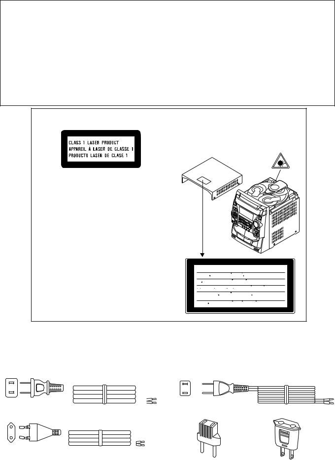
Figure 2 AC POWER SUPPLY CORD AND AC PLUG ADAPTOR
– 2 –
CD-K7000V,CP-C7000
FOR A COMPLETE DESCRIPTION OF THE OPERATION OF THIS UNIT, PLEASE REFER TO THE OPERATION MANUAL.
SPECIFICATIONS
CD-K7000V
General
Power source: |
AC 110/127/220/230-240 V, 50/60 |
|
|
|
Hz |
|
|
|
Power |
210 W |
|
consumption: |
|
|
|
|
|
Dimensions: |
Width; 270 mm (10-5/8") |
|
|
|
Height; 330 mm (13") |
|
|
Depth; 355 mm (14") |
|
|
|
Weight: |
11.5 kg (25.3 lbs.) |
|
|
|
|
|
Amplifier section |
|
|
||
|
||
|
|
|
Output power: |
MPO; 830 W (415 W + 415 W) (10 |
|
|
|
% T.H.D.) |
|
|
RMS; 500 W (250 W + 250 W) (10 |
|
|
% T.H.D.) |
|
|
RMS; 440 W (220 W + 220 W) (0.9 |
|
|
% T.H.D.) |
|
|
|
Input terminals: |
Video/Auxiliary (audio signal) x 1; |
|
|
|
500 mV/47 kohms |
|
|
Microphone 1/2; 1 mV/600 ohms |
|
|
|
Output terminals: |
Speakers; 6 ohms |
|
|
|
Headphones; 16 - 50 ohms (rec- |
|
|
ommended; 32 ohms) |
|
|
Video out; 1 Vp-p (75 ohms) |
|
|
|
|
Compact disc player section |
|
|
||
|
||
|
|
|
Type: |
3-disc multi-play compact disc |
|
|
|
player |
|
|
|
Signal readout: |
Non-contact, 3-beam semi-con- |
|
|
|
ductor laser pickup |
|
|
|
D/A converter: |
1-bit D/A converter |
|
|
|
|
Frequency |
20 - 20,000 Hz |
|
response: |
|
|
|
|
|
Dynamic range: |
90 dB (1 kHz) |
|
|
|
|
Video CD section
Video output format: PAL/PAL 60/NTSC
Tuner section
|
Frequency range: |
FM; 88 - 108 MHz |
||
|
|
|
AM; 531 - 1,602 kHz |
|
|
|
|
|
|
|
|
Cassette deck section |
||
|
|
|||
|
|
|||
|
|
|
|
|
|
Frequency |
50 - 14,000 Hz (Normal tape) |
||
|
response: |
|
|
|
|
|
|
|
|
|
Signal/noise ratio: |
55 dB (TAPE 1, playback) |
||
|
|
|
50 dB (TAPE 2, recording/play- |
|
|
|
|
back) |
|
|
|
|
|
|
|
Wow and flutter: |
0.3 % (WRMS) |
||
|
|
|
|
|
|
|
|
|
|
|
|
CP-C7000 |
|
|
|
|
|
|
|
|
Type: |
4-way type [25 cm (10") woofer, |
||
|
|
|
10cm (4") midrange, 10 cm (4") |
|
|
|
|
tweeter and super tweeter] |
|
|
|
|
|
|
|
Maximum input |
500 W |
||
|
power (total): |
|
|
|
|
|
|
|
|
|
Rated input power |
250 W |
||
|
(total): |
|
|
|
|
|
|
|
|
|
Impedance: |
6 ohms |
||
|
|
|
|
|
|
Dimensions: |
Main speaker |
||
|
|
|
Width; 330 mm (13") |
|
|
|
|
Height; 330 mm (13") |
|
|
|
|
Depth; 386 mm (15-3/8") |
|
|
|
|
Sub speaker |
|
|
|
|
Width; 330 mm (13") |
|
|
|
|
Height; 135 mm (5-5/16") |
|
|
|
|
Depth; 306 mm (12-1/4") |
|
|
|
|
|
|
|
Weight: |
Main speaker |
||
|
|
|
8.8 kg (19.4 lbs.)/each |
|
|
|
|
Sub speaker |
|
|
|
|
3.8 kg (8.4 lbs.)/each |
|
|
|
|
|
|
Specifications for this model are subject to change without prior notice.
– 3 –
CD-K7000V,CP-C7000
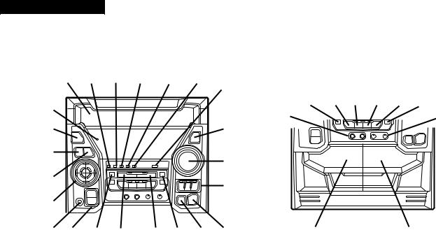
NAMES OF PARTS
CD-K7000V
 Front panel
1 |
2 |
3 |
4 |
5 |
6 |
7 |
|
|
|
|
|
|
|
|
|
24 25 26 27 28 29 |
|||
8 |
|
|
|
|
|
|
|||
|
|
|
|
|
14 |
30 |
|
31 |
|
9 |
|
|
|
|
|
|
|||
|
|
|
|
|
|
|
|
||
10 |
|
|
|
|
|
15 |
|
|
|
11 |
|
|
|
|
|
|
|
|
|
|
|
|
|
|
16 |
|
|
|
|
12 |
|
|
|
|
|
|
|
|
|
|
|
|
|
|
|
|
|
|
|
13 |
|
19 |
|
20 21 22 |
23 |
|
32 |
33 |
|
17 18 |
|
|
|||||||
1. Disc Tray |
|
|
|
|
|
24. |
(TAPE 2) |
Record Pause Button |
|
2. (VCD/CD) Karaoke Mode Button |
|
25. |
(TAPE 2) |
Reverse Play Button |
|
||||
3. (VCD) Playback Control Button |
|
|
26. |
(VCD) Stop/Return Button |
|
||||
4. (VCD) On Screen Display On/Off Button |
|
|
(CD/TAPE) Stop Button |
|
|||||
5. (VCD) Digest Button |
|
|
|
|
27. |
(TAPE 2) |
Reverse Mode Button |
|
|
6. (VCD) Bookmark Button |
|
|
|
28. |
(VCD/CD) Play/Repeat Button |
|
|||
7. Surround Button |
|
|
|
|
|
|
(TAPE 1) |
Play Button |
|
8. Timer Set Indicator |
|
|
|
|
|
(TAPE 2) |
Forward Play Button |
|
|
9. On/Stand-by Button |
|
|
|
|
29. Extra Bass/Demo Mode Button |
|
|||
10. Clock Button |
|
|
|
|
|
30. Microphone Sockets |
|
||
11. Timer/Sleep Button |
|
|
|
|
31. Microphone Level Controls |
|
|||
12. Function Selector Buttons |
|
|
|
32. |
(TAPE 1) |
Cassette Compartment |
|||
13. Headphone Socket |
|
|
|
|
33. |
(TAPE 2) |
Cassette Compartment |
||
14.Dimmer Button
15.Volume Control
16.(VCD/CD) Disc Number Select Buttons
17.Tuning and Time Up/Down Buttons
18.Memory/Set Button
19.(VCD) Skip/Previous Button (CD) Track Down/Review Button (TUNER) Preset Down Button (TAPE 2) Fast Wind Button
20.(VCD) Skip/Next Button (CD) Track Up/Cue Button (TUNER) Preset Up Button (TAPE 2) Fast Wind Button
21.Equalizer Mode Selector Button
22.(VCD/CD) Disc Skip Button
23.(VCD/CD) Open/Close Button
– 4 –
CD-K7000V,CP-C7000
 Display
1 |
7 |
8 |
9 |
10 |
11 |
12 |
4 5 6 |
2 |
3 |
2 |
13 14 15 16 |
17 18 19 |
|
|
|
1. Extra Bass Indicator |
10. |
(VCD/CD) More Tracks Indicator |
|
2. Spectrum Analyzer/Volume Level Indicator |
11. Sleep Indicator |
||
3. |
(VCD/CD) Disc Number Indicators |
12. FM Stereo Mode Indicator |
|
4. Karaoke Mode Indicator |
13. |
(TAPE) Reverse Mode Indicator |
|
5. |
(VCD/CD/TUNER) Memory Indicator |
14. |
(TAPE 2) Reverse Play Indicator |
6. |
(VCD/CD) Pause Indicator |
15. (TAPE 1) Play Indicator |
|
7. |
(TAPE 2) Record Indicator |
|
(TAPE 2) Forward Play Indicator |
8. |
(VCD/CD) Play Indicator |
16. |
(VCD/CD) Repeat Indicator |
9. |
(VCD/CD) Music Schedule Indicators |
17. FM Stereo Indicator |
|
|
|
18. Timer Record Indicator |
|
|
|
19. Timer Play Indicator |
|
 Rear panel
|
3 |
|
|
4 |
|
|
5 |
|
1 |
6 |
|
7 |
||
|
||
2 |
8 |
|
9 |
1.AC Voltage Selector
2.AC Power Lead
3.FM 75 Ohms Aerial Terminal
4.FM Aerial Earth Terminal
5.AM Loop Aerial Input Socket
6.Span Selector Switch
7.Video/Auxiliary (Audio Signal) Input Sockets
8.Video Output Socket
9.Main Speaker Terminals
– 5 –
CD-K7000V,CP-C7000
|
1 |
2 |
9 |
3 |
|
4
5
6


 10
10
7


8 |
|
|
|
11 12 13 14 |
|
15 |
21 |
|
22 |
||
16 |
||
23 |
||
17 |
||
24 |
||
18 |
||
25 |
||
19 |
||
26 |
||
20 |
||
27 |
||
|
||
|
28 |
CP-C7000
2
1 |
3 |
4
|
|
|
|
|
|
|
|
|
|
|
|
|
|
|
|
|
|
|
|
|
|
|
|
|
|
|
|
|
|
|
|
|
|
|
|
|
|
|
|
|
|
|
|
|
|
|
|
|
|
|
|
|
|
|
|
|
|
|
|
|
|
|
|
|
|
|
|
|
|
|
|
|
|
|
|
|
|
|
|
|
|
|
|
|
1 |
2 |
3 |
4 |
|
|
5 |
|
|
|
|||||||
 Remote control
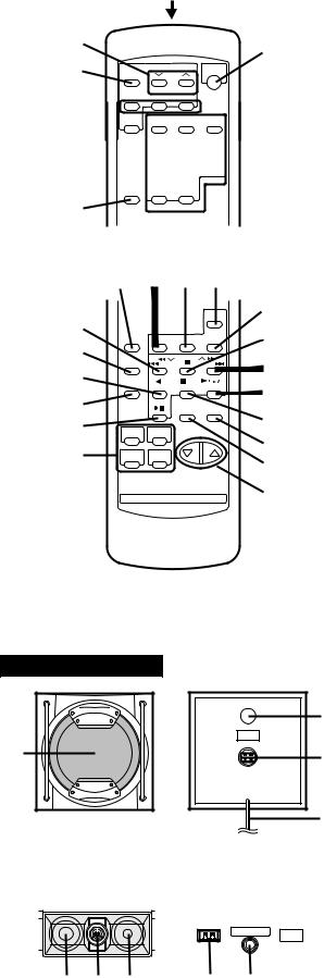
1.Remote Control Transmitter LED
2.Echo Level Up/Down Buttons
3.Karaoke Mode Button
4.Key Control Buttons
5.Vocal Replacer Button
6.(VCD) VCD Auto/On Button
7.(VCD) Playback Control Auto/Off Button
8.(VCD) On Screen Display On/Off Button
9.On/Stand-by Button
10.(VCD) Direct Search Button
11.(VCD) Digest/Time Search Button
12.(VCD/CD) Clear Button
13.(VCD/CD) Memory Button
14.(VCD/CD) Disc Skip Button
15.(VCD) Skip/Previous Button (CD) Track Down/Review Button (TUNER) Preset Down Button (TAPE 2) Fast Wind Button
16.(VCD) Bookmark Button
17.(TAPE 2) Reverse Play Button
18.(VCD) PAL/NTSC Select Button
19.(TAPE 2) Record Pause Button
20.Function Selector Buttons
21.(VCD/CD) Random Button
22.(VCD/CD) Pause Button
23.(VCD) Skip/Next Button (CD) Track Up/Cue Button (TUNER) Preset Up Button
(TAPE 2) Fast Forward Button
24.(VCD) Play/Repeat/Select/Resume Button (CD) Play/Repeat Button
(TAPE 1) Play Button (TAPE 2) Fast Wind Button
25.(VCD) Stop/Return Button (CD/TAPE) Stop Button
26.Extra Bass Button
27.Equalizer Mode Selector Button
28.Volume Up/Down Buttons
 Main Speaker
1.Woofer
2.Bass Reflex Duct
3.Speaker Terminals
4.Speaker Wire for Sub Speaker
 Sub Speaker
1.Midrange
2.Super Tweeter
3.Tweeter
4.Speaker Terminals
5.Bass Reflex Duct
– 6 –
– 7 –
PREPARATION FOR USE
 Connecting the AC power lead
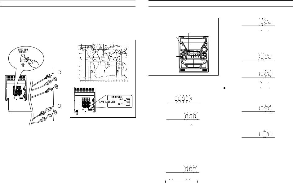
Check the setting of the AC voltage selector located on the rear panel before plugging the unit into an AC socket. If necessary, adjust the selector to correspond to the AC power voltage used in your area.
Selector adjustment:
Turn the selector with a screwdriver until the appropriate voltage number appears in the window (110V, 127V, 220V or 230V - 240V AC).
 1
1
 2
2
To an AC socket
Notes:
 Plug the AC power lead into an AC socket, after any connections.
 Unplug the AC power lead from the AC socket if the unit will not be in use for a prolonged period of time.
AC Plug Adaptor
In areas (or countries) where an AC socket as shown in illustration  is used, connect the unit using the AC plug adaptor supplied with the unit, as illustrated. The AC plug adaptor is not included in areas where the AC wall socket and AC power plug can be directly connected (see illustration
  ).
).
 AM/FM interval (span)
The International Telecommunication Union (ITU) has established that member countries should maintain either a 10 kHz or a 9 kHz interval between broadcasting frequencies of any AM station. The illustration shows the 9 kHz interval zones (regions 1 and 3), and the 10 kHz interval zone (region 2).
Before using the unit, set the SPAN SELECTOR switch (on the rear panel) to AM tuning interval (span) of your area.
To change the tuning zone:
1 Press the ON/STAND-BY button to enter the standby mode.
2 Set the SPAN SELECTOR switch to "50/9" for 9 kHz AM interval (50 kHz FM interval), and "100/10" for 10 kHz AM interval (100 kHz FM interval).
3 Whilst pressing down the  button and the X-BASS/ DEMO button, hold down the ON/STAND-BY button for at least 1 second.
 "CLEAR AL" will appear.
Caution:
 The operation explained above will erase all data stored in memory including clock and timer settings, and tuner and CD presets.
SETTING THE CLOCK
In this example, the clock is set for the 24-hour (0:00) system.
(Main unit operation)
MEMORY/SET
ON/
STAND-BY
CLOCK 
TUNING/ TIME
( )
)
1 Press the ON/STAND-BY button to enter the standby mode.
2 Press the CLOCK button.
3 Within 5 seconds, press the MEMORY/SET button.
4 Press the TUNING/TIME ( or ) button to select the time display mode.
"0:00"  The 24-hour display will appear. (0:00 - 23:59)
"AM 0:00"  The 12-hour display will appear. (AM 0:00 - PM 11:59)
"AM 12:00"  The 12-hour display will appear. (AM 12:00 - PM 11:59)
 Note that this can only be set when the unit is first installed or it has been reset.
0:00 AM 0:00 AM 12:00
5 |
Press the MEMORY/SET button. |
6 |
Press the TUNING/TIME ( or ) button to adjust |
|
the hour. |
 Press the TUNING/TIME (
 or
or  ) button once to advance the time by 1 hour. Hold it down to advance continuously.
 When the 12-hour display is selected, "AM" will change automatically to "PM".
7 Press the MEMORY/SET button.
8 Press the TUNING/TIME ( |
or |
) button to adjust |
OPERATION |
the minutes. |
|
|
|
Press the TUNING/TIME ( |
or |
) button once to |
|
advance the time by 1 minute. Hold it down to change the time in 5-minute intervals.
 The hour setting will not advance even if minutes advance from "59" to "00".
9 |
Press the MEMORY/SET button. |
MANUAL |
|
 The clock starts operating from "0" second. (Seconds are not displayed.) And then the clock display will disappear after a few seconds.
To see the time display:
Press the CLOCK button.
The time display will appear for about 5 seconds.
Note:
 The clock display will flash on and off at the push of the CLOCK button when the AC power supply is restored after a power failure occurs or after the AC power lead is disconnected. If this happens, follow the procedure below to change the clock time.
To change the clock time:
1Press the CLOCK button.
2Within 5 seconds, press the MEMORY/SET button.
3Perform steps 6 - 9 above.
To change the time display mode:
1Perform steps 1 - 2 in "RESETTING THE MICROCOMPUTER".
2Perform steps 1 - 9 above.
C7000-K7000V,CP-CD
REMOTE CONTROL
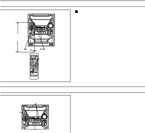
0.2 m - 6 m (8" - 20')
15 |
15 |
|
Remote control
Notes concerning use:
 Replace the batteries if the operating distance is reduced or if the operation becomes erratic.
 Periodically clean the transmitter LED on the remote control and the sensor on the main unit with a soft cloth.
 Exposing the sensor on the main unit to strong light may interfere with operation. Change the lighting or the direction of the unit.
 Keep the remote control away from moisture, excessive heat, shock, and vibrations.
– 8 –
RESETTING THE MICROCOMPUTER
2
1
Reset the microcomputer under the following conditions:
 To erase all of the stored memory contents (clock and timer settings, and tuner and CD presets).
 If the display is not correct.
 If the operation is not correct.
1 Press the ON/STAND-BY button to enter the standby mode.
2 Whilst pressing down the  button and the X-BASS/ DEMO button, hold down the ON/STAND-BY button for at least 1 second.
 "CLEAR AL" will appear.
Caution:
 The operation explained above will erase all data stored in memory including clock and timer settings, and tuner and CD presets.
C7000-K7000V,CP-CD
CD-K7000V,CP-C7000
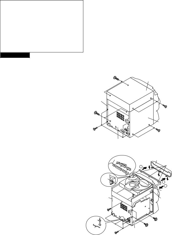
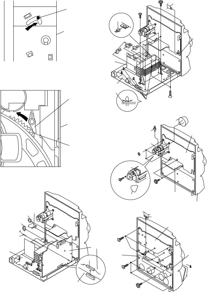
DISASSEMBLY
Caution on Disassembly
Follow the below-mentioned notes when disassembling the unit and reassembling it, to keep it safe and ensure excellent performance:
1.Take cassette tape and compact disc out of the unit.
2.Be sure to remove the power supply plug from the wall outlet before starting to disassemble the unit.
3.Take off nylon bands or wire holders where they need to be removed when disassembling the unit. After servicing the unit, be sure to rearrange the leads where they were before disassembling.
4.Take sufficient care on static electricity of integrated circuits and other circuits when servicing.
CD-K7000V
STEP |
REMOVAL |
|
PROCEDURE |
|
FIGURE |
|
|
|
|
|
|
1 |
Top Cabinet |
1. Screw ..................... |
(A1) x4 |
9-1 |
|
|
|
|
|
|
|
2 |
Side Panel |
1. Screw ..................... |
(B1) x8 |
9-1 |
|
|
(Left/Right) |
|
|
|
|
|
|
|
|
|
|
3 |
CD Player Unit/ |
1. |
Turn on the power supply, |
9-2 |
|
|
CD Tray Cover |
|
open the disc tray, take out |
|
|
|
|
|
the CD cover, and close. |
|
|
|
|
|
(Note 1) |
|
|
|
|
2. |
Screw ..................... |
(C1) x1 |
|
|
|
3. |
Hook ....................... |
(C2) x3 |
|
|
|
4. |
Hook ....................... |
(C3) x2 |
|
|
|
5. |
Socket .................... |
(C4) x3 |
|
4 |
Rear Panel |
1. Screw ..................... |
(D1) x7 |
9-2 |
|
|
|
2. |
Socket .................... |
(D2) x1 |
|
|
|
|
|
|
|
5 |
Main PWB |
1. Screw ..................... |
(E1) x1 |
9-2 |
|
|
|
2. |
Socket .................... |
(E2) x4 |
10-3,4 |
|
|
3. |
Flat Cable ............... |
(E3) x1 |
10-3 |
|
|
4. |
Tip Wire .................. |
(E4) x1 |
|
|
|
|
|
|
|
6 |
Power Amp. PWB |
1. |
Screw ..................... |
(F1) x5 |
10-4 |
|
|
2. |
Socket .................... |
(F2) x3 |
|
|
|
3. |
Flat Wire ................. |
(F3) x1 |
|
|
|
4. |
PWB Holder ........... |
(F4) x4 |
|
|
|
|
|
|
|
7 |
Front Panel |
1. Screw ..................... |
(G1) x3 |
10-4 |
|
|
|
|
|
|
|
8 |
Volume Mechanism/ |
1. |
Knob ....................... |
(H1) x1 |
10-5 |
|
Volume Motor |
2. Screw ..................... |
(H2) x4 |
|
|
|
|
3. |
Socket .................... |
(H3) x1 |
|
|
|
4. |
Belt ......................... |
(H4) x1 |
|
|
|
5. |
Screw ..................... |
(H5) x2 |
|
|
|
|
|
|
|
9 |
Karaoke PWB |
1. Screw ..................... |
(J1) x2 |
10-5 |
|
|
|
|
|
|
|
10 |
Display PWB |
1. Screw ..................... |
(K1) x11 |
10-6 |
|
|
|
2. |
Flat Cable ............... |
(K2) x1 |
|
|
|
|
|
|
|
11 |
Tape Mechanism |
1. |
Open the cassette holder. |
10-6 |
|
|
|
2. |
Screw...................... |
(L1) x5 |
|
|
|
|
|
|
|
12 |
Headphones PWB |
1. |
Screw ..................... |
(M1) x1 |
10-6 |
|
|
|
|
|
|
13 |
Turntable |
1. Hook ....................... |
(N1) x2 |
11-1 |
|
|
|
2. |
Cover ..................... |
(N2) x1 |
|
|
|
|
|
|
|
14 |
Disc Tray |
1. |
Turn fully the lock lever in the |
10-1 |
|
|
|
|
arrow direction. |
|
|
|
|
2. |
While holding the lock lever, rotate |
10-2 |
|
|
|
|
the cam gear until the cam gear |
|
|
|
|
|
rib engages with the clamp lever. |
|
|
|
|
3. |
Push the slide holder backward to |
11-2 |
|
|
|
|
engage the claw with the groove |
|
|
|
|
|
and remove it in the direction |
|
|
|
|
|
of the arrow. .............. |
(P1) x6 |
|
|
|
|
|
|
|
15 |
CD Video PWB |
1. Screw ..................... |
(Q1) x1 |
11-3 |
|
|
(Note 2) |
2. Hook ....................... |
(Q2) x2 |
|
|
|
|
3. |
Socket .................... |
(Q3) x4 |
|
|
|
|
|
|
|
STEP |
REMOVAL |
|
PROCEDURE |
FIGURE |
|
|
|
|
|
16 |
CD Mechanism |
1. Hook |
....................... (R1) x2 |
11-4 |
|
|
2. Hook ....................... |
(R2) x3 |
|
|
|
|
|
|
17 |
Loading Motor PWB |
1. Hook ....................... |
(S1) x5 |
11-4 |
|
|
|
|
|
Note 1:
How to open the changer manually. (Fig. 10-1)
1.In this state, turn fully the lock lever in the arrow direction through the hole on the loading chassis bottom.
2.While holding the lock lever, rotate the cam gear anticlockwise until the cam gear rib engages with the clamp lever. (Fig. 10-2)
3.After that, push forward the CD slide holder.
Note 2:
1.After removing the connector for the optical pickup from the connector, wrap the conductive aluminium foil around the
front end of the connector to protect the optical pickup from electrostatic damage.
Note 3:
1.Be careful not to break the claw of the CD mechanism.
2.When fining back the cam gear assembly, let it lock by front movement.
(A1)x2 |
Top Cabinet |
|
ø3x12mm |
||
|
Side Panel (Right)
(B1)x2 |
|
|
|
ø3x10mm |
|
(A1)x2 |
|
|
|
|
ø3x12mm |
|
|
|
Side Panel |
|
|
|
(Left) |
|
(B1)x4 |
|
(B1)x2 |
|
ø3x10mm |
|
|
|
|
ø3x10mm |
|
|
|
|
|
|
|
Rear |
|
|
|
Panel |
|
|
|
Figure 9-1 |
|
|
|
CD Video |
CD Tray Cover |
|
|
PWB |
|
|
|
|
|
|
|
(C4)x3 |
(C2) x3 |
|
|
|
|
|
|
|
1 |
|
(C3) x1 |
|
|
|
Pull |
|
1 |
|
|
|
2 |
|
|
|
CD Player |
|
Rear |
|
Unit |
|
|
(C3)x1 |
|
|
Panel |
|
|
|
(C1)x1 |
|
|
|
ø3x10mm |
|
|
(D2)x1 |
|
(E1)x1 |
|
|
ø3x6mm |
||
|
|
|
|
|
|
|
(D1)x2 |
Power Amp. |
Main PWB |
ø3x10mm |
|
PWB |
(D1)x5 |
|
|
|
|
|
|
ø3x10mm
Figure 9-2
– 9 –
CD-K7000V,CP-C7000
Figure 10-1
Figure 10-2
(E3)x1 (E2)x1 
(E2)x1
(E4)x1
Power
Amp.
PWB
Figure 10-3
|
(F1)x3 |
|
|
ø3x10mm |
(F3)x1 |
|
(F1)x2 |
|
Lock Lever |
|
|
ø3x6mm |
|
|
|
|
|
|
(E2)x1 |
|
CD Player Unit |
|
Headphones |
(Bottom View) |
(F2)x3 |
PWB |
|
|
|
|
Power |
|
|
Supply |
|
|
PWB |
|
Power |
|
|
|
Amp. |
|
(G1)x3 |
|
PWB |
|
||
Clamp Lever |
Push |
ø3x10mm |
|
(F4)x4 |
|||
|
|
Figure 10-4
CD Player Unit
(Top View)
Cam Gear Rib
Main PWB
(E2)x1
Power
Supply
PWB
|
(H1)x1 |
(H3)x1 |
Display |
PWB |
|
Volume |
|
Mechanism |
|
(H2)x4  ø3x12mm
Volume
Motor
(H5)x2 |
(J1)x2 |
|
ø2x5mm |
||
ø3x10mm |
||
|
||
(H4)x1 |
Karaoke |
|
PWB |
||
|
||
|
Front Panel |
|
|
Figure 10-5 |
|
|
(K2)x1 |
|
|
Display PWB |
|
(K1)x11 |
|
|
ø3x10mm |
|
|
Tape |
Headphones |
|
PWB |
||
Mechanism |
||
|
||
(L1)x5 |
Open |
|
ø3x10mm |
|
|
|
Cassette |
|
|
Holder |
|
(M1)x1 |
|
|
ø3x10mm |
|
Figure 10-6
– 10 –
(N2)x1
Turntable
Slide
Chassis
(N1)x2
CD Player Unit
Figure 11-1
(P1)x3
|
|
3 |
|
|
|
2 |
|
|
|
1 |
|
|
|
|
|
|
(P1)x3 |
|
|
|
|
Figure 11-2 |
|
|
|
CP-C7000 |
|
|
|
STEP |
REMOVAL |
PROCEDURE |
|
FIGURE |
1 |
Woofer |
1. Front Panel ............ |
(A1) x1 |
11-5 |
|
|
2. Screw ..................... |
(A2) x8 |
11-6 |
2 |
Tweeter |
1. Front Panel ............ |
(B1) x1 |
12-1 |
|
|
2. Screw ..................... |
(B2) x4 |
12-2 |
3 |
Mid Range |
1. Screw ..................... |
(C1) x4 |
12-2 |
4 |
Super Tweeter |
1. Screw ..................... |
(D1) x2 |
12-2 |
(A1) x1
Screwdriver
Driver should be pried away
from speaker box.
Figure 11-5
CD-K7000V,CP-C7000
(Q1)x1 |
CD Video |
Slide |
|
ø3x8mm |
|||
Chassis |
|||
|
PWB |
||
|
|
||
(Q3)x2 |
|
|
(Q2)x2
(Q3)x2
Figure 11-3
CD |
(R2)x3 |
|
Mechanism |
|
|
|
|
Loading |
|
(R1)x1 |
Motor |
(R1)x1 |
PWB |
(S1)x5
Figure 11-4
Caution:
The metallic handles on the both sides of the speaker grill on the main speaker are decorations.
Do not carry the speakers by them as this may damage the speakers.
(A2) x8 ø4x16mm
Woofer
Front
Panel
Figure 11-6
– 11 –
CD-K7000V,CP-C7000
Screwdriver
Mid
Range
(C1)x4
ø4x16mm
(B1)x1 |
(B2)x4 |
|
ø4x16mm |
Super |
Tweeter |
|
(D1)x2 |
||
Tweeter |
||
ø3x10mm |
Driver should be pried away
from speaker box.

 Front
Front
Panel
Figure 12-1 |
Figure 12-2 |
REMOVING AND REINSTALLING THE MAIN PARTS
TAPE MECHANISM SECTION
Perform steps 1 to 7 and 11 of the disassembly method to remove the tape mechanism.
How to remove the record/playback and erase heads (TAPE 2) (See Fig. 12-3)
1.When you remove the screws (A1) x 2 pcs., the recording/ playback head and three-dimensional head of the erasing head can be removed.
How to remove the playback head (TAPE 1) (See Fig. 12-4)
1.When you remove the screws (B1) x 2 pcs., the playback head.
How to remove the pinch roller (TAPE 1/2) (See Fig. 12-5)
1.Carefully bend the pinch roller pawl in the direction of the arrow <A>, and remove the pinch roller (C1) x 1 pc., in the direction of the arrow <B>.
Note:
When installing the pinch roller, pay attention to the spring mounting position.
|
|
Pinch |
Pinch Roller |
Roller |
|
Pawl |
||
(C1)x1 |
Pull |
Pull <A> |
|
|
|
<B>
Figure 12-5
TAPE 2
Record/Playback
Head
Erase Head
(A1)x2
Ø2x6mm
Figure 12-3
TAPE 1
Playback
Head
(B1)x1
Ø2x9mm
 (B1)x1 Ø2x5mm
Figure 12-4
– 12 –
CD-K7000V,CP-C7000
How to remove the belt (TAPE 2) (See Fig. 13-1)
1.Remove the main belt (D1) x 1 pc., from the motor side.
2.Remove the FF/REW belt (D2) x 1 pc.
How to remove the belt (TAPE 1) (See Fig. 13-1)
1. Remove the main belt (E1) x 1 pc., from the motor side. 2. Remove the FF/REW belt (E2) x 1 pc.
How to remove the motor (See Fig. 13-2)
1. Remove the screws (F1) x 2 pcs., to remove the motor.
Motor
|
|
Motor |
|
TAPE 2 |
FF/REW |
Motor |
TAPE 1 |
|
|||
|
Belt |
TAPE 2 |
Main Belt |
|
(D2)x1 |
(E1)x1 |
|
|
Main Belt |
||
|
|
|
|
|
|
(D1)x1 |
|
(F1) x2
Ø2.6x5mm
 TAPE 1 (D1)x1
FF/REW Belt
 (E2)x1 (E1)x1
Figure 13-1 |
Figure 13-2 |
CD MECHANISM SECTION
Perform steps 1, 2, 3, 13 and 16 of the disassembly method to remove the CD mechanism.
How to remove the loading motor (See Fig. 13-3)
1.Bend the hooks (A1) x 5 pcs., to remove the loading motor.
2.Remove the drive belt (A2) x1.
How to remove the pickup (See Fig. 13-4)
1.Remove the stop washer (B1) x 1 pc., to remove the gear (B2).
2.Remove the screws (B3) x 2 pcs., to remove the shaft (B4).
3.Remove the pickup.
Note
After removing the connector for the optical pickup from the connector, wrap the conductive aluminium foil around the front end of connector to protect the optical pickup from electrostatic damage.
– 13 –
Slide Chassis |
Loading Motor |
(A1)x3
(A1)x2
Pulley Motor
Drive Belt (A2) x1
|
Figure 13-3 |
|
(B3) x2 |
Stop Washer |
|
(B1) x1 |
||
ø2.6 x6mm |
||
|
Pickup
Shaft |
CD Mechanism |
|
Gear |
||
(B4) x1 |
||
(B2) x1 |
||
|
||
|
Figure 13-4 |
CD-K7000V,CP-C7000
ADJUSTMENT
MECHANISM SECTION
∙ Driving Force Check
Torque Meter |
Specified Value |
|
|
Play: TW-2111 |
Tape 1: Over 80 g |
|
Tape 2: Over 80 g |
|
|
∙ Torque Check
Torque Meter |
Specified Value |
|
|
|
|
|
Tape 1 |
Tape 2 |
|
|
|
Play: TW-2111 |
30 to 80 g.cm |
30 to 80 g.cm |
|
|
|
Fast forward: TW-2231 |
— |
70 to 180 g.cm |
|
|
|
Rewind: TW-2231 |
— |
70 to 180 g.cm |
|
|
|
∙ Tape Speed
|
Test Tape |
Adjusting |
Specified |
Instrument |
|
|
Point |
Value |
Connection |
|
|
|
|
|
Normal |
MTT-111 |
Variable |
3,000 ± 30 Hz |
Speaker |
speed |
|
Resistor in |
|
terminal |
|
|
motor. |
|
(Load |
|
|
(MM1) |
|
resistance: |
|
|
|
|
6 ohms) |
|
|
|
|
|
TAPE MECHANISM
Motor
Variable Resistor in motor
Figure 14-1
TUNER SECTION |
|
|
|
|
|
|
|
∙ FM RF |
|
|
|
|
|
|
|
|
|
|
|
|
||||||||
fL: Low-range frequency |
|
|
|
|
|
|
|
Signal generator: 1 kHz, 75 kHz dev., FM modulated |
||||||||||||||||||||
|
|
|
|
|
|
|
|
|
|
|
|
|
|
|
|
|
|
|
|
|
|
|
||||||
fH: High-range frequency |
|
|
|
|
|
|
|
Test Stage |
Frequency |
Frequency |
Setting/ |
Instrument |
||||||||||||||||
∙ AM IF/RF |
|
|
|
|
|
|
|
|
|
|
|
|
|
|
|
|
|
|
|
|
|
|
|
Display |
Adjusting |
Connection |
||
Signal generator: 400 Hz, 30%, AM modulated |
|
|
|
|
|
|
|
|
|
|
|
|
|
|
|
|
|
|
|
Point |
|
|||||||
|
|
|
|
|
FM Band |
|
— |
|
|
|
88.00 MHz |
T301(fL): |
*1 |
|||||||||||||||
|
|
|
|
|
|
|
|
|
|
|
|
|
|
|
|
|
||||||||||||
Test Stage |
Frequency |
Frequency |
|
Setting/ |
|
|
Instrument |
|
|
|
|
|
|
|||||||||||||||
|
|
|
|
|
Coverage |
|
|
|
|
|
|
|
|
|
|
|
1.3 V ± 50 mV |
|
||||||||||
|
|
|
|
Display |
|
Adjusting |
|
Connection |
|
|
|
|
|
|
|
|
|
|
|
|
|
|
|
|
|
|
||
|
|
FM RF |
|
98.00 MHz |
98.00 MHz |
L312 |
*2 |
|||||||||||||||||||||
|
|
|
|
|
|
Parts |
|
|
|
|
|
|
||||||||||||||||
|
|
|
|
|
|
|
|
|
|
|
|
|
|
|
|
|
(10-30 dB) |
|
|
|
|
|
||||||
AM IF |
450 kHz |
|
1,602 kHz |
|
T351 |
|
|
*1 |
|
|
|
|
|
|
|
|
|
|
|
|||||||||
|
|
|
|
|
|
|
|
|
|
|
|
|
|
|
|
|
|
|
|
|
|
|||||||
|
|
|
|
|
|
|
|
|
|
|
|
|
*1. Input: Antenna |
|
|
Output: TP301 |
|
|||||||||||
AM Band |
— |
|
531 kHz |
|
(fL): T306 |
|
*2 |
|
|
|
||||||||||||||||||
Coverage |
|
|
|
|
|
1.1 ± 0.1 V |
|
|
|
*2. Input: Antenna |
|
|
Output: Speaker terminal |
|
||||||||||||||
|
|
|
|
|
|
|
|
|
|
|
|
|
|
|
|
|
|
|
|
|
|
|
|
|
|
|
|
|
AM Tracking |
990 kHz |
|
990 kHz |
|
(fL): T303 |
|
*1 |
|
|
|
|
|
|
|
|
|
|
|
|
|
|
|
|
|
|
|||
|
|
|
|
|
|
|
|
|
|
|
|
|
|
|
|
|
|
|
|
|
|
|
|
|
|
|
|
|
*1. Input: Antenna |
Output: TP302 |
|
|
|
|
|
|
|
|
|
|
|
|
|
|
|
|
|
|
|
|
|
|
|
||||
*2. Input: Antenna |
Output: TP301 |
|
|
|
CNP301 |
|
|
|
|
|
|
|
|
|
|
|
|
|
|
|
|
|||||||
|
|
|
|
SO302 |
|
|
|
|
|
|
|
|
|
|
|
|
|
|
|
|
|
|
|
|||||
|
|
|
|
|
|
AM LOOP |
|
|
|
|
|
|
|
|
|
|
|
|
|
|
|
|
||||||
|
|
|
|
FM ANTENNA |
|
|
|
|
|
|
|
|
|
|
|
|
|
|
|
|
||||||||
|
|
|
|
ANTENNA |
|
|
|
|
|
|
|
|
|
|
|
|
|
|
|
|
||||||||
|
|
|
|
|
|
|
|
|
|
|
|
|
|
TUNER PWB |
|
|
|
|
|
|
||||||||
|
|
|
|
|
|
|
|
|
1 |
|
T303 |
|
|
|
|
|
|
|
|
|
|
|
|
|||||
|
|
|
|
|
|
|
|
|
|
|
|
AM |
|
|
|
|
|
|||||||||||
|
|
|
|
|
|
|
|
|
|
IC301 |
|
|
L312 |
|
|
TRACKING fL |
|
|
|
|
||||||||
|
|
|
|
|
|
|
|
|
|
|
|
|
|
|
|
|
|
|||||||||||
|
|
|
|
|
|
|
|
|
|
T302 |
|
|
|
|
|
|
||||||||||||
|
|
|
|
|
|
|
|
|
|
|
|
|
|
|
|
|
|
|
|
|
|
|
||||||
|
|
|
|
|
|
|
|
|
|
|
|
|
|
|
|
|
|
|
|
|
|
|
||||||
|
|
|
|
TP301 |
|
|
|
|
|
|
|
|
|
|
|
|
|
T306 |
|
|
|
|
|
|||||
|
|
|
|
|
|
|
|
|
|
FM IF |
|
|
|
|
|
|
|
|
|
|
|
|
|
|
|
|||
|
|
|
|
|
|
R382 |
|
|
|
FM RF |
|
|
|
|
|
|
|
|
|
|
|
|
|
|||||
|
|
|
|
|
|
T301 |
|
|
|
|
|
|
|
|
|
|
|
|
|
|
|
|
||||||
|
|
|
|
|
|
|
|
|
|
|
|
|
|
|
|
|
|
|
|
|
|
|
|
|||||
|
|
|
|
|
|
|
|
|
|
|
|
|
|
|
|
AM BAND |
|
|
|
|||||||||
|
|
|
|
FM BAND |
|
|
|
|
|
|
|
|
|
|
|
|
|
|||||||||||
|
|
|
|
|
|
|
|
|
|
|
|
|
|
|
|
|
|
|
COVERAGE fL |
|
|
|
||||||
|
|
|
|
COVERAGE fL |
|
|
|
T351 |
|
|
|
|
|
|
|
|
|
|
|
|||||||||
|
|
|
|
|
|
|
|
|
|
|
|
|
|
|
|
|
|
|
|
|
|
|
||||||
|
|
|
|
|
|
|
|
|
|
|
|
|
|
|
|
|
|
|
|
|
||||||||
|
|
|
|
|
|
|
|
|
|
|
|
|
|
|
|
|
|
|
|
|
|
|
|
|
|
|||
AM IF
TP302
 R357
R357
Figure 14-2 ADJUSTMENT POINTS
– 14 –
CD SECTION
•Adjustment
Since this CD system incorporates the following automatic adjustment functions, readjustment is not needed when replacing the pickup. Therefore, different PWBs and pickups can be combined freely.
Each time a disc is changed, these adjustments are performed automatically. Therefore, playback of each disc can be performed under optimum conditions.
Items adjusted automatically
(1)Offset adjustment (The offset voltage between the head amplifier output and the VREF reference voltage is compensated inside the IC.)
*Focus offset adjustment
*Tracking offset adjustment
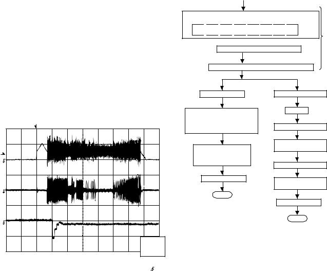
(2)Tracking balance adjustment (waveform drawing Fig. 15 EFBL)
(3)Gain adjustment (The gain is compensated inside the IC so that the loop gain at the gain crossover frequency will be 0 dB.)
*Focus gain adjustment
*Tracking gain adjustment
|
Stopped |
|
T |
|
|
|
|
|
1999/04/05 |
20:26:47 |
|
|
|
|
|
|
|
|
|||
|
CH1=500mV |
CH2=200mV |
CH3=1V |
|
|
500ms/div |
||||
|
DC |
10:1 |
|
DC |
10:1 |
DC 10:1 |
|
|
(500ms/div) |
|
|
|
|
|
|
|
NORM:20kS/s |
||||
T |
FDO |
|
|
|
|
|
|
|
|
|
|
|
|
|
|
|
|
|
|
|
|
1 |
|
|
|
|
|
|
|
|
|
|
3 |
TE |
|
|
|
|
|
|
|
|
|
|
|
|
|
|
|
|
|
|
|
|
|
EFBL |
|
|
|
|
|
|
|
|
|
2 |
|
|
|
|
|
|
|
|
|
|
|
|
|
|
|
|
|
|
|
|
CH2 |
|
|
|
|
|
|
|
|
|
|
v/DIV |
|
|
|
|
|
|
|
|
|
|
200mV |
|
=Filter= |
|
|
=Offset= |
=Record Length= |
|
=Trigger= |
|||
Smoothing : |
ON |
CH1 : |
0.000V |
Main : |
100K |
Mode : SINGLE |
||||
BW |
: FULL |
|
CH2 : |
0.000V |
Zoom : |
2k |
Type |
: EDGE CH1 |
||
|
|
|
CH3 : |
0.00V |
|
|
Delay : |
0.0ns |
||
|
|
|
CH4 : |
0.00V |
|
|
Hold off : |
0.2 s |
||
Figure 15
CD ERROR CODE DESCRIPTION
Error |
State Code |
|
|
|
[Servo System Error] |
0001 |
Cannot detect Pickup-in SW |
0002 |
DSP access error |
|
|
|
[Error during close operation] |
0101 |
Open/Close SW not functioning (Low → High) |
0103 |
Open/Close SW not functioning (High → Low) |
|
|
|
[Error during open operation] |
0201 |
Open/Close SW not functioning (Low → High) |
0203 |
Open/Close SW not functioning (High → Low) |
|
|
|
[Error during skip operation] |
0302 |
Pickup-in SW is not detected |
0306 |
During Disc 1 search, Open/Close SW or Clamp SW |
|
or Disc SW do not change to low. |
0307 |
Clamp SW not function (Low → High) |
0308 |
Clamp SW not function (High → Low) |
|
|
CD-K7000V,CP-C7000
TEST MODE
·Setting the test mode
Any one of test mode can be set by pressing several keys as follows.
<X-BASS> + <CD> + <POWER> TEST:CD operation test
Function:-CD test mode. -Enter test mode.
C
 D
D 


 T
T 
 E
E 
 S
S 
 T
T 

IL isn't don
OPEN/CLOSE operation is using manual.
<< >>, <<
 >> buttons make pick's slide possible.
<<PLAY>> key input.
Do TOC IL. Do normal play When these following key is input into PLAY key, track number can be appoint directly
<< 1>> key: Track 4 <<
 2>> key: Track 9 <<
 3>> key: Track 15
<<STOP>> key input.
STOP
VOL — Last memory
BAL — CENTER
P.GEQ — FLAT
X-BASS — OFF
<<MEMORY>> key input.
Laser ON.
<<MEMORY>> key input.
Tracking OFF play at that specific point.
<<MEMORY>> key input.
Tracking ON play at that specific point.
<<STOP>> key input.
STOP
Sliding the PICKUP with << >>, <<
 >> button
must only be in STOP mode.
To cancel : Power OFF
– 15 –
CD-K7000V,CP-C7000
NOTES ON SCHEMATIC DIAGRAM
∙Resistor:
To differentiate the units of resistors, such symbol as K and M are used: the symbol K means 1000 ohm and the symbol M means 1000 kohm and the resistor without any symbol is ohm-type resistor. Besides, the one with “Fusible” is a fuse type.
∙Capacitor:
To indicate the unit of capacitor, a symbol P is used: this symbol P means micro-micro-farad and the unit of the capacitor without such a symbol is microfarad. As to electrolytic capacitor, the expression “capacitance/withstand voltage” is used.
(CH), (TH), (RH), (UJ): Temperature compensation (ML): Mylar type
(P.P.): Polypropylene type
∙Schematic diagram and Wiring Side of P.W.Board for this model are subject to change for improvement without prior notice.
∙The indicated voltage in each section is the one measured by Digital Multimeter between such a section and the chassis with no signal given.
1.In the tuner section, ( ) indicates AM
< > indicates FM stereo
2.In the main section, a tape is being played back.
3.In the deck section, a tape is being played back. ( ) indicates the record state.
4.In the power section, a tape is being played back.
5.In the CD section, the CD is stopped.
∙Parts marked with “ ” (
” ( 


 ) are important for maintaining the safety of the set. Be sure to replace these parts with specified ones for maintaining the safety and performance of the set.
REF. NO |
DESCRIPTION |
POSITION |
|
|
|
SW1 |
OPEN/CLOSE |
ON—OFF |
|
|
|
SW2 |
CLAMP |
ON—OFF |
|
|
|
SW3 |
DISC NUMBER |
ON—OFF |
|
|
|
SW4 |
PICKUP IN |
ON—OFF |
|
|
|
SW601 |
SPAN SELECTOR |
9 kHz/50 kHz— |
|
|
10 kHz/100 kHz |
|
|
|
SW701 |
ON/STAND-BY |
ON—OFF |
|
|
|
SW702 |
CLOCK |
ON—OFF |
|
|
|
SW703 |
TIMER/SLEEP |
ON—OFF |
|
|
|
SW704 |
KARAOKE MODE |
ON—OFF |
|
|
|
SW705 |
P.B.O |
ON—OFF |
|
|
|
SW706 |
OSD |
ON—OFF |
|
|
|
SW707 |
DIGEST |
ON—OFF |
SW708 |
BOOK MARK |
ON—OFF |
|
|
|
SW709 |
DISC 1 |
ON—OFF |
|
|
|
SW710 |
DISC 2 |
ON—OFF |
|
|
|
SW711 |
DISC 3 |
ON—OFF |
|
|
|
SW712 |
DISC SKIP |
ON—OFF |
|
|
|
SW713 |
OPEN/CLOSE |
ON—OFF |
|
|
|
SW714 |
DIMMER |
ON—OFF |
|
|
|
REF. NO |
DESCRIPTION |
POSITION |
|
|
|
SW715 |
X-BASS/MEMO |
ON—OFF |
|
|
|
SW716 |
EQUALIZER |
ON—OFF |
|
|
|
SW717 |
SURROUND |
ON—OFF |
SW718 |
REV MODE |
ON—OFF |
|
|
|
SW719 |
CD |
ON—OFF |
|
|
|
SW723 |
TAPE |
ON—OFF |
SW724 |
TUNING DOWN |
ON—OFF |
|
|
|
SW725 |
MEMORY/SET |
ON—OFF |
|
|
|
SW726 |
TRACK DOWN/REVIEW/ |
ON—OFF |
|
PRESET DOWN/REWIND |
|
|
|
|
SW727 |
TRACK UP/CUE/PRESET UP/ |
ON—OFF |
|
FAST FORWARD |
|
|
|
|
SW728 |
PLAY |
ON—OFF |
SW729 |
STOP |
ON—OFF |
|
|
|
SW730 |
REVERSE PLAY |
ON—OFF |
|
|
|
SW731 |
REC PAUSE |
ON—OFF |
SW732 |
TUNING/TIME UP |
ON—OFF |
|
|
|
SW733 |
VIDEO/AUX |
ON—OFF |
|
|
|
SW734 |
TUNER (BAND) |
ON—OFF |
|
|
|
SW801 |
VOLTAGE SELECTOR |
230-240—220 |
|
|
—127—110 |
|
FRONT |
|
|
|
|
|
|
|
|
|
|
3 |
|
|
FRONT |
||||||||||
|
|
FRONT |
|
|
|
|
|
||||||||||||||||||
|
|
|
VIEW |
|
|
|
|
|
|
|
|
||||||||||||||
|
|
|
|
|
|
|
|
|
|
|
VIEW |
|
|
TOP |
|
|
VIEW |
||||||||
|
|
|
|
|
|
|
|
|
|
|
|
|
|
|
|
|
|
|
VIEW |
|
|
|
|
|
|
|
|
|
|
|
|
|
|
|
|
|
|
|
|
|
|
|
|
|
|
|
|
|
|
|
|
|
|
|
|
|
|
|
|
|
|
|
|
|
|
|
|
|
|
|
|
|
|
|
|
|
|
|
|
E |
C B |
|
|
|
|
|
|
|
|
|
|
|
|
|
|
|
|
||||||
|
(S) (G) (D) |
B C E |
2 |
1 |
|
|
|
|
|
|
|||||||||||||||
|
|
|
|
|
|
|
|||||||||||||||||||
(1) |
(2) (3) |
|
|
|
|
|
|
|
|||||||||||||||||
|
KTC2026 |
|
KTA1298 Y |
|
|
|
|
|
|||||||||||||||||
2SA1015 GR |
KTC3194 Y |
|
|
|
|
|
|
||||||||||||||||||
|
|
|
|
|
|
|
|
KTA1504 GR |
|
|
|
|
|
||||||||||||
2SC1845 F |
|
|
|
KTC3203 Y |
|
|
|
|
|
|
|
|
4204SRT7 |
||||||||||||
|
|
|
|
|
|
|
|
|
|
|
KTC3265 Y |
||||||||||||||
2SK246 GR |
|
|
|
KRA107 M |
|
|
|
|
|
|
|
|
4204UGT7 |
||||||||||||
|
|
|
|
|
|
|
|
|
|
|
|
|
|
||||||||||||
KTA1266 GR |
KRC102 S |
|
|
|
|
|
|
|
|
|
|
|
4204UYT7 |
||||||||||||
KTA1271 Y |
|
|
|
KRC104 S |
|
|
|
|
|
|
|
|
|
|
|
|
|
|
|
|
|||||
KTA1273 Y |
KRC102 M |
|
|
|
|
|
|
|
|
|
|
|
|
|
|
|
|
||||||||
KTA1274 Y |
|
|
|
KRC104 M |
|
|
|
|
|
|
|
|
|
|
|
|
|
|
|
|
|||||
KTC3199 GR |
KRC107 M |
|
|
|
|
|
|
|
|
|
|
|
|
|
|
|
|
||||||||
Figure 16 TYPES OF TRANSISTOR AND LED
– 16 –
|
|
|
|
|
|
|
|
|
|
|
|
|
|
|
|
|
|
|
|
|
|
|
|
|
|
|
|
|
|
|
|
|
|
|
|
|
CD-K7000V,CP-C7000 |
||||
|
|
|
|
|
|
|
|
|
|
|
|
|
|
|
XV2 |
|
|
|
|
|
|
|
|
|
|
|
|
|
|
|
|
|
|
|
|
|
|
|
|
|
|
|
|
|
|
|
|
|
|
|
|
|
|
|
|
|
27MHz |
|
|
|
|
|
|
|
|
|
|
|
|
|
|
|
|
+B3 |
|
|
|
|
|
|
|
|
|
|
|
|
|
|
|
|
|
|
|
|
|
|
|
|
|
|
|
|
|
|
|
|
|
|
|
|
|
|
|
|
|
|
XV1 |
|
|
|
|
|
|
||
|
|
|
|
|
|
|
|
|
|
|
|
|
|
|
|
|
|
|
|
|
|
|
|
|
|
|
|
|
|
|
|
|
|
|
|
|
|
|
|
||
|
|
|
|
|
|
|
|
|
|
|
|
|
|
|
|
|
|
10~ 7 |
5 |
|
~ |
2 |
|
|
|
|
|
|
|
|
4.19MHz |
|
|
|
|
|
|
||||
|
|
|
|
|
|
21 27 35 45 |
|
|
|
|
|
|
14 |
13 |
|
|
|
|
|
|
|
|
|
|
|
|
|
|
|
|
|
|
|||||||||
|
|
|
|
|
|
|
|
|
73 |
MD8 |
|
X2 |
X1 |
|
HD0 |
~ |
HD3 |
HD4 |
|
|
HD7 |
18 |
|
|
|
|
|
|
|
|
|
|
|
|
|
|
|
||||
|
|
|
|
|
|
|
|
|
|
|
|
|
|
|
|
|
|
|
|
|
10 24 35 |
40 |
41 |
|
|
|
|
|
|
||||||||||||
|
|
|
|
|
|
|
|
|
|
DQ15 |
39 |
~70 |
~ |
|
|
|
|
|
|
|
|
|
|
|
|
|
|
|
|||||||||||||
|
|
|
|
|
|
|
|
|
|
~ |
~ |
MD11 |
|
|
|
|
|
|
|
|
|
|
|
57 HD0 |
VDD0 |
VDD1 AVDD |
X2 |
X1 |
|
|
|
|
|
|
|||||||
|
|
|
|
|
|
|
|
|
|
DQ12 36 |
68 |
MD12 |
|
|
|
|
|
|
|
|
|
|
|
|
|
|
|
|
|
|
|
50 |
|
|
|
||||||
|
|
|
|
|
|
|
|
|
|
DQ11 34 |
~ |
MD15~ |
|
|
|
|
|
|
|
|
|
|
|
|
92 |
|
|
|
|
~64~HD7 |
|
|
|
|
|
||||||
|
|
|
|
|
|
|
|
|
|
|
|
|
|
|
|
|
|
|
|
|
|
|
|
|
|
|
~ |
|
|
|
|||||||||||
|
|
|
|
|
|
|
|
|
|
~ ~ |
|
|
|
|
|
|
|
|
|
|
|
|
84 |
|
|
|
|
|
|
|
|
||||||||||
|
|
|
|
|
|
|
|
|
|
DQ8 31 |
65 |
|
|
|
ICV2 |
|
|
|
|
|
|
|
|
|
|
|
|
|
|
|
|
|
|
|
45 |
|
|
|
|||
|
|
|
|
|
|
|
|
|
|
62 |
MD0 |
|
|
|
|
|
|
|
|
|
|
83 |
|
|
|
|
|
|
|
|
|
|
|
|
|
|
|||||
|
|
|
|
|
|
|
|
|
|
|
|
|
|
|
|
|
|
|
|
|
|
|
|
|
|
|
|
|
|
|
42 |
|
|
|
|||||||
|
|
|
|
|
|
|
|
|
|
A8 26 |
~ |
~ |
|
D61012GC |
|
|
|
|
|
76 |
|
|
|
|
|
|
|
|
|
|
|
|
|
|
|||||||
|
|
|
|
|
|
|
|
|
|
|
~ |
58 |
MD4 |
|
|
|
|
|
|
|
|
|
|
|
|
ICV1 |
|
|
|
33 |
|
|
|
||||||||
|
|
|
|
|
|
|
|
|
|
|
|
|
|
|
|
|
75 |
|
|
|
|
|
|
|
|
|
|
|
|
||||||||||||
|
|
|
|
|
|
|
|
|
|
|
56 |
MD5 |
|
|
|
|
|
|
|
|
|
|
|
|
|
|
|
|
|
|
|
|
~ |
|
|
|
|||||
|
|
|
|
|
|
|
|
|
|
A4 22 |
MPEG DECODER |
|
|
|
|
|
|
|
|
|
|
|
|
|
|
|
|
||||||||||||||
|
|
|
|
|
|
|
|
|
|
A3 19 |
~ |
~ |
|
|
63 |
|
|
|
|
MPEG CONTROLLER |
25 |
|
|
|
|||||||||||||||||
|
|
|
|
|
|
|
|
|
|
~ ~ |
54 |
MD7 |
|
|
|
|
|
|
|
|
|
|
|
|
51 |
|
|
|
|
17 |
|
|
|
||||||||
|
|
|
|
|
|
|
|
|
|
A0 16 |
53 |
MCAS |
|
|
|
|
|
|
|
|
|
|
|
|
44 |
|
|
|
|
|
IX0352AW |
|
|
16 |
|
|
|
||||
|
|
|
|
|
|
|
|
|
|
RAS 14 |
52 |
MWE |
|
|
|
|
|
|
|
|
|
|
|
|
36 |
|
|
|
|
|
|
|
|
|
|
14 |
|
|
|
||
|
|
|
|
|
20 |
|
|
|
|
WE 13 |
49 |
MRAS |
|
|
|
|
|
|
|
|
|
|
|
|
25 |
|
|
|
|
|
|
|
|
|
|
|
9 |
|
|
|
|
|
|
|
|
|
6 |
VDD |
ICV3 |
SDM4260C |
DRAM |
DQ7 10 |
48 |
MA0 |
|
|
|
|
|
|
|
|
|
|
VDD,CKSEL,HSELX, HSELA,AVDD ~ |
|
|
|
|
|
PWR MPEG |
|
|
|
|
~ |
|
|
|
||||
|
|
|
|
|
~ ~ |
|
~ |
|
|
|
|
AULRCK |
CDC2PO CDLRCK |
|
|
|
23 |
|
|
|
|
|
|
|
|
|
|
7 |
|
|
|
||||||||||
|
|
|
|
|
1 |
45 |
|
|
|
|
|
|
|
|
|
|
|
|
|
|
|
|
|
|
|
|
|||||||||||||||
|
|
|
|
|
DQ4 |
7 |
MA3 |
VOUT1 |
|
AUDO |
AUBCK |
CDBCK |
|
17 |
|
|
|
|
|
|
SBUSY |
|
|
MBUSY |
|
|
|
|
|||||||||||||
|
|
|
|
|
|
DQ3 |
5 |
42 |
MA4 |
|
CDI |
~ |
|
|
|
|
|
|
MDI |
MDO MCK |
|
|
|
|
|||||||||||||||||
|
|
|
|
|
|
~ ~ |
~ |
~ |
|
15 |
|
|
|
|
|
|
|
|
|
|
|||||||||||||||||||||
|
|
|
|
|
|
|
1 |
|
|
|
|
|
|
|
|
|
|
||||||||||||||||||||||||
|
|
|
|
|
|
|
|
|
|
DQ0 |
2 |
38 |
MA8 |
86 |
|
35 32 |
33 95 97 98 99 |
|
|
|
|
|
15 |
|
44 |
18 19 20 22 |
|
|
|
|
|||||||||||
|
|
|
|
|
|
|
|
|
|
|
|
|
|
|
|
|
|
|
|
|
|
|
|
|
|
||||||||||||||||
|
|
|
|
|
|
|
|
|
NJM2267M VIDEO OPERATION AMP. |
|
|
|
|
|
|
|
|
|
|
|
|
|
|
|
|
|
|
|
|
QV2 |
QV3 |
|
|
|
|
|
|
|
|
||
|
|
|
|
|
CNPV3 |
|
ICV4 |
|
|
|
|
|
|
|
|
|
|
|
|
|
|
|
|
|
|
|
|
|
|
|
|
|
|
|
|
|
|
|
|||
|
|
JK671 |
1 |
|
6 |
1 |
|
|
|
|
|
|
|
|
|
|
|
|
|
|
|
|
|
|
|
|
|
|
|
|
|
|
|
|
|
|
|||||
|
|
VIDEO |
|
|
|
|
|
|
|
|
|
|
|
|
|
|
|
|
|
|
|
|
+B5 |
|
|
|
|
|
|
|
|
|
|
||||||||
|
|
2 |
|
|
|
|
|
|
|
|
|
|
|
|
|
|
|
|
|
|
|
|
|
|
|
|
|
|
|
|
|
|
|||||||||
|
|
OUT |
|
|
|
|
|
|
|
|
|
|
|
|
|
|
|
|
|
|
|
|
|
|
|
|
|
|
|
|
|
|
|
|
|
|
|||||
|
|
|
|
|
|
|
2 |
|
|
|
|
|
|
|
|
|
|
|
|
|
|
|
|
|
|
|
|
|
|
|
|
|
|
|
|
|
|
|
|||
|
|
|
|
|
|
|
|
|
|
|
|
|
|
|
|
|
|
|
|
|
|
|
|
|
|
|
|
|
|
|
|
|
|
|
|
|
|
|
|||
|
|
|
|
|
|
|
|
|
7 |
|
|
|
|
|
|
|
|
|
|
|
|
|
|
|
|
|
|
|
|
|
|
|
|
|
|
|
|
|
|
|
|
|
|
|
|
|
|
|
|
|
+B3 |
|
|
|
|
|
|
|
|
|
|
|
|
|
|
|
|
|
|
|
|
|
|
|
|
|
|
|
|
|
|
|
|
|
|
|
|
|
|
|
|
|
|
|
|
|
|
|
|
|
|
|
|
|
|
|
|
|
|
|
|
|
|
|
|
|
|
|
|
|
|
|
|
|
SW4 |
|
|
|
|
|
|
|
|
|
|
|
|
|
|
|
|
|
|
|
|
|
|
|
|
|
|
|
|
|
|
|
|
|
|
|
|
|
|
|
|
|
PICKUP IN |
|
|
M3 |
|
|
|
|
|
|
|
|
|
|
|
|
|
|
|
|
|
|
|
|
|
|
|
|
|
|
|
|
|
|
|
|
|
|
|
|
|
|
|
|
|
T/T |
|
|
|
|
|
|
|
|
|
|
|
|
|
|
|
|
|
|
|
|
|
|
|
|
|
|
|
|
|
|
|
|
|
|
|
|
|
|
|
|
UP/DOWN |
BI4 |
CNS4 CNP4 |
|
|
|
|
|
|
|
|
|
|
|
|
|
|
|
|
|
|
|
|
|
|
|
|
|
|
|
|
|
|
|
|
|
|
||||
|
MOTOR |
|
|
|
|
|
|
|
|
|
|
|
|
|
|
|
|
|
|
|
|
|
|
|
|
|
|
|
|
|
|
|
|
|
|
|
|
|
|
|
|
SW3 |
|
- |
|
6 |
6 |
|
6 |
|
|
|
|
|
|
|
|
|
|
|
|
|
|
|
|
|
|
|
|
|
|
|
|
|
|
|
|
|
|
|
|
|
|
|
M |
|
|
|
|
|
|
|
|
|
|
|
|
|
|
|
|
|
|
|
|
|
|
|
|
|
|
|
|
|
|
35 |
29 |
22 |
21 |
14 |
8 |
|
|
|
|
DISC |
|
|
5 |
5 |
|
5 |
|
|
|
|
|
|
|
|
|
|
|
|
|
|
|
|
|
|
|
|
|
|
|
|
|
|
|
|
|||||||
NUMBER |
+ |
|
|
|
|
|
|
|
|
|
|
|
|
|
|
|
|
|
|
|
|
|
|
|
|
|
|
|
|
|
|
|
|
|
|
|
|||||
|
|
4 |
4 |
|
4 |
|
|
|
|
|
|
|
|
|
|
|
|
|
|
|
|
|
|
|
|
|
|
|
LOADING M+ |
|
|
|
|
FOCUS/TRACKING/ SPIN/SLED DRIVER |
SP- |
27 |
|
|
|||
|
|
|
|
|
|
|
|
|
|
|
|
|
|
|
|
|
|
|
|
|
|
|
|
|
|
|
|
|
|
|
|
|
|
||||||||
SW2 |
|
|
|
|
|
|
|
|
|
|
|
|
|
|
|
|
|
|
|
|
|
|
|
|
|
|
|
39 |
|
|
|
|
|
|
|
||||||
|
|
|
|
|
|
|
|
|
|
|
|
|
|
|
|
|
|
|
|
|
|
|
|
|
|
|
|
|
|
|
|
|
|
SP+ |
26 |
|
|
||||
CLAMP |
|
|
3 |
3 |
|
3 |
|
|
|
|
|
|
|
|
|
|
|
|
|
|
|
|
|
|
|
|
|
|
|
LOADING M- |
38 |
|
|
|
|
|
|||||
|
|
|
|
|
|
|
|
|
|
|
|
|
|
|
|
|
|
|
|
|
|
|
|
|
|
|
|
|
|
M63001FP |
SL+ |
16 |
|
|
|||||||
|
|
|
|
|
|
|
|
|
|
|
|
|
|
|
|
|
|
|
|
|
|
|
|
|
|
|
|
|
|
|
|
|
|
|
|
||||||
|
|
|
|
2 |
2 |
|
2 |
|
|
|
|
|
|
|
|
|
|
|
|
|
|
|
|
|
|
|
|
|
|
|
LD_M+ |
|
|
|
|
|
|||||
|
|
|
|
|
|
|
|
|
|
|
|
|
|
|
|
|
|
|
|
|
|
|
|
|
|
|
|
42 |
|
|
SL- |
15 |
|
|
|||||||
|
|
|
|
1 |
1 |
|
1 |
|
|
|
|
|
|
|
|
|
|
|
|
|
|
|
|
|
|
|
|
|
|
|
LD_M- |
|
|
|
|
||||||
SW1 |
|
|
|
|
|
|
|
|
|
|
|
|
|
|
|
|
|
|
|
|
|
|
|
|
|
|
41 |
|
|
|
|
|
|
||||||||
|
|
|
|
|
|
|
|
|
|
|
|
|
|
|
|
|
|
|
|
|
|
|
|
|
|
|
|
|
|
|
|
|
|
|
|
||||||
OPEN/ |
|
|
|
|
|
|
|
|
|
|
|
|
|
|
|
|
|
|
|
|
|
|
|
|
|
|
|
|
|
|
|
|
TR- |
7 |
|
|
|||||
CLOSE |
|
|
|
|
|
|
|
|
|
|
|
|
|
|
|
|
|
|
|
|
|
|
|
|
|
|
|
|
|
25 |
SPDO |
|
|
||||||||
|
|
|
|
|
|
|
|
|
|
|
|
|
|
|
|
|
|
|
|
|
|
|
|
|
|
|
|
|
|
|
|
|
|
|
|
||||||
|
|
|
|
|
|
|
|
|
|
|
|
|
|
|
|
|
|
|
|
|
|
|
|
|
|
|
|
|
|
|
|
17 |
SLDO |
IC3 |
TR+ |
6 |
|
|
|||
|
|
|
|
|
|
|
|
|
|
|
|
|
|
|
|
|
|
|
|
|
|
|
|
|
|
|
|
|
|
|
|
FO- |
5 |
|
|
||||||
|
|
|
|
|
|
|
|
|
|
|
|
|
|
|
|
|
|
|
|
|
|
|
|
|
|
|
|
|
|
|
|
2 |
FD |
|
|
|
|
|
|
||
|
|
|
|
|
|
|
|
|
|
|
|
|
|
|
|
|
|
|
|
|
|
|
|
|
|
|
|
|
|
|
|
VCC1 |
VCC4 |
VCC2 |
|
FO+ |
4 |
|
|
||
|
|
|
|
|
|
|
|
|
|
|
|
|
|
|
|
|
|
|
|
|
|
|
|
|
|
|
|
|
|
|
|
1 |
TO |
|
|
|
|||||
|
|
CNP12 |
|
|
|
|
|
|
|
|
|
|
|
|
|
|
|
|
|
|
|
|
|
|
|
|
|
|
|
VCC3 |
|
|
|
||||||||
|
MBUSY 12 |
|
|
|
|
|
|
|
|
|
|
|
|
|
|
|
|
|
|
|
|
|
|
|
|
|
|
|
|
|
18 |
40 |
24 |
23 |
28 |
|
M |
M |
|||
|
|
|
|
|
|
|
|
|
|
|
|
|
|
|
|
|
|
|
|
|
|
|
|
|
|
|
|
|
|
|
|
|
|
|
|
||||||
|
SBUSY |
11 |
|
|
|
|
|
|
|
|
|
|
|
|
|
|
|
|
|
|
|
|
|
|
|
|
|
|
|
|
|
|
|
|
|
|
|
||||
|
|
|
|
|
|
|
|
|
|
|
|
|
|
|
|
|
|
|
|
|
|
|
|
|
|
|
|
|
|
|
|
+5V |
|
|
|
|
|
||||
|
|
GND |
10 |
|
|
|
|
|
|
|
|
|
|
|
|
|
|
|
|
|
|
|
|
|
|
|
|
|
|
|
|
|
|
|
|
|
|
M1 |
M2 |
||
|
|
|
|
|
|
|
|
|
|
|
|
|
|
|
|
|
|
|
|
|
|
|
|
|
|
|
|
|
|
|
|
|
|
|
|
SLED |
|||||
|
|
|
|
|
|
|
|
|
|
|
|
|
|
|
|
|
|
|
|
|
|
|
|
|
|
|
|
|
|
|
|
|
|
|
|
|
|
|
|
SPINDLE |
|
CLAMP SW |
|
9 |
|
|
|
|
|
|
|
|
|
|
|
|
|
|
|
|
|
|
|
|
|
|
|
|
|
|
|
|
|
|
|
|
|
|
|
MOTOR |
MOTOR |
||
SECTION |
CD RES |
|
8 |
|
|
|
|
|
|
|
|
|
|
|
|
|
|
|
|
|
|
|
|
|
|
|
|
|
|
|
|
|
|
|
|
|
|
|
|
|
|
|
CLK |
|
7 |
|
|
|
|
|
|
|
|
|
|
|
|
|
|
|
|
|
|
|
|
|
|
|
|
|
|
|
|
|
|
|
|
|
|
|
|
|
|
|
|
|
6 |
|
|
|
|
|
|
|
|
|
|
|
|
|
|
|
|
|
|
|
|
|
|
|
|
|
|
|
|
|
|
|
|
|
|
|
|
|
|
DISPLAY |
|
DI |
|
|
|
|
|
|
|
|
|
|
|
|
|
|
|
|
|
|
|
|
|
|
|
|
|
|
|
|
|
|
|
|
|
|
|
|
|
|
|
|
DO |
|
5 |
|
|
|
|
|
|
|
|
|
|
|
|
|
|
|
|
|
|
|
|
|
|
|
|
|
|
|
|
|
|
|
|
|
|
+3.3V |
TRACKING COIL |
||
|
CE |
|
4 |
|
|
|
|
|
|
|
|
|
|
|
|
|
|
|
|
|
|
|
|
|
|
|
|
|
|
|
|
|
|
|
|
|
|
|
|||
TO |
|
|
|
|
|
|
|
|
|
|
|
|
|
|
|
|
|
|
|
|
|
|
|
|
|
|
|
|
|
|
|
|
|
|
LASER |
|
FOCUS COIL |
||||
|
DRF |
|
3 |
|
|
|
|
|
|
|
|
|
|
|
|
|
|
|
|
|
|
|
|
|
|
|
|
|
|
|
|
|
|
|
|
Q3 |
|||||
|
|
|
|
|
|
|
|
|
|
|
|
|
|
|
|
|
|
|
|
|
|
|
|
|
|
|
|
|
|
|
|
|
|
|
|||||||
|
|
|
|
|
|
|
|
|
|
|
|
56 |
55 54 35 |
57 |
~ |
59 |
|
33 |
|
26 |
25 |
24 |
23 |
|
|
|
|
|
|
|
DRIVER |
|
|
||||||||
|
|
WRQ |
|
2 |
|
|
|
|
|
|
|
|
40 |
|
|
|
|
|
|
|
|
|
|
|
|
|
|
||||||||||||||
|
|
|
|
|
|
|
|
|
|
|
|
|
|
|
|
|
|
|
|
CONT5 |
|
|
|
|
|
19 |
|
|
|
|
|
|
|
|
|
|
|
||||
|
|
|
|
|
|
|
|
|
|
|
|
|
|
|
|
|
|
|
|
|
|
|
|
|
|
|
|
|
|
|
|
|
|
|
|
|
|
||||
|
|
|
|
|
|
|
|
|
|
|
|
|
|
|
|
|
|
|
|
|
|
|
|
|
|
|
|
|
|
|
|
|
|
|
|
|
|
|
|||
|
|
CDINT |
|
1 |
|
|
|
|
|
|
|
|
30 |
CONT2 |
|
|
|
|
|
|
|
|
SLD0 |
SPD0 |
FD0 |
TD0TE 16 |
|
|
|
|
|
|
|
|
|
|
|
||||
|
|
|
|
|
|
|
|
|
|
|
|
|
31 |
CONT3 |
|
|
|
|
|
|
|
|
|
|
|
|
|
|
|
|
|
|
|
||||||||
|
|
|
|
|
|
|
|
|
|
|
|
|
|
|
|
|
|
|
|
|
|
|
|
|
|
FE 15 |
|
|
22 |
RFEV |
|
|
|
|
|
|
|||||
|
|
|
|
|
|
|
|
|
|
|
|
|
|
|
|
|
|
|
|
|
|
|
|
|
|
|
|
|
|
|
|
|
|
|
|
|
|||||
|
|
CNP11 |
|
|
|
|
|
|
|
Q2 |
32 |
CONT4 |
|
|
|
|
|
|
|
|
|
|
|
|
|
|
|
|
FE- |
|
|
|
|
|
|
|
|||||
|
|
|
|
|
|
|
|
|
|
|
|
|
|
|
|
|
|
|
|
|
|
RFEV 14 |
|
|
21 |
|
|
|
|
|
|
|
|||||||||
+5V(+B5) |
|
5 |
|
|
|
|
|
|
|
|
|
|
|
|
|
|
|
|
|
|
|
|
|
|
|
|
|
|
|
|
|
|
|
|
|
|
|
||||
|
|
|
|
|
|
|
|
|
|
|
|
|
|
|
|
|
|
|
|
|
|
|
|
|
|
|
|
|
20 |
FE |
|
|
|
|
|
|
|
||||
MAINSECTION (TO IC401) |
|
|
|
|
|
|
|
|
|
|
|
|
48 |
RCHO |
|
|
|
|
|
|
|
|
|
|
|
|
|
HFL |
7 |
|
|
|
|
|
|
LDD |
8 |
|
|||
|
DGND |
|
4 |
|
|
|
|
|
|
|
|
|
|
|
|
|
IC2 |
|
|
|
|
|
|
|
|
|
|
|
|
|
|||||||||||
|
|
|
|
|
|
|
|
|
|
|
|
RFEV |
|
|
|
|
|
|
|
|
|
|
|
|
19 |
TE- |
|
|
|
|
|
7 |
|
||||||||
|
L-CH |
|
3 |
|
|
|
|
|
|
|
|
47 |
RVSS |
|
|
LC78636E |
|
|
|
3 |
|
|
18 |
TE |
|
IC1 |
|
PD |
|
||||||||||||
|
|
|
|
|
|
|
|
|
|
46 |
LVSS |
|
SERVO DSP |
|
|
XVDD 50 |
|
|
|
|
|
|
|
||||||||||||||||||
|
AGND |
|
2 |
|
|
|
|
|
|
|
|
|
|
|
|
|
17 |
HFL |
LA9235M |
|
4 |
|
|||||||||||||||||||
|
|
|
|
|
|
|
|
|
|
45 |
LCHO |
|
|
|
|
|
|
|
|
|
|
|
|
RVDD 49 |
|
|
TIN2 |
|
|||||||||||||
TO |
|
|
|
|
|
|
|
|
|
|
|
|
|
|
|
|
|
|
|
|
|
|
|
|
|
|
|
|
SERVO AMP. |
|
|
||||||||||
|
|
|
1 |
|
|
|
|
|
|
|
|
|
|
|
|
|
|
|
|
|
|
|
|
|
|
|
|
|
|
|
|
|
|
3 |
|
||||||
|
R-CH |
|
|
|
|
|
|
|
|
|
|
|
|
|
|
|
|
|
|
|
|
|
|
|
|
|
LVDD |
44 |
+3.3V |
|
|
|
|
|
|
|
TIN1 |
|
|||
|
|
|
|
|
|
|
|
|
|
|
53 |
|
|
|
|
|
|
|
|
|
|
|
|
|
|
|
|
|
|
|
|
|
|
|
|||||||
|
|
|
|
|
|
|
|
|
|
|
|
|
|
|
|
|
|
|
|
|
|
|
|
|
|
|
|
|
|
|
|
|
|
|
|
|
FIN2 |
2 |
|
||
|
|
|
|
|
|
|
|
|
|
|
|
|
|
|
|
|
|
|
|
|
|
|
|
|
|
|
|
VDD |
36 |
|
|
|
|
|
|
|
|
|
|||
|
|
|
|
|
|
|
|
|
|
|
|
|
|
|
|
|
|
|
|
|
|
|
|
|
|
|
|
|
|
|
|
|
|
|
|
|
|
||||
|
|
|
|
|
|
|
|
|
|
|
|
|
76 |
CONT7 |
|
|
|
|
|
|
|
|
|
|
|
|
ADAVDD 18 |
|
|
|
|
VCC |
|
|
FIN1 |
1 |
|
||||
|
|
|
|
|
|
|
|
|
|
|
|
|
|
|
|
|
|
|
|
|
|
|
|
|
|
|
|
|
VVDD |
5 |
|
|
|
|
|
|
|
|
|
||
|
|
|
|
|
|
|
|
|
|
|
|
|
75 |
CONT6 |
|
|
|
|
|
|
|
|
|
|
|
|
|
|
|
|
|
30 |
23 |
11 |
9 |
|
|
||||
|
|
|
|
|
|
|
|
|
|
|
|
|
|
|
|
|
|
|
|
|
WRQ |
|
|
RES |
|
|
XOUT |
|
XIN VDD5V |
|
|
|
|
|
|
|
|||||
|
|
|
|
|
|
|
|
|
|
|
|
|
|
CE |
CL |
DI |
DO |
INT |
|
|
|
|
DEF |
|
73 |
+5V |
|
|
|
|
|
|
|
|
|
|
|||||
|
|
|
|
|
|
|
|
|
|
|
|
|
|
|
|
|
|
|
|
|
|
|
|
|
|
|
|
|
|
||||||||||||
|
|
|
|
|
|
|
|
|
|
|
|
|
|
65 |
66 |
67 |
68 |
69 |
|
70 |
|
71 |
72 |
52 |
|
51 |
|
|
|
|
|
|
|
|
|
|
|
|
|||
|
|
|
|
|
|
|
|
|
|
|
|
|
|
|
|
|
|
|
|
|
|
|
|
|
|
|
|
|
|
|
|
|
Q1 |
|
|
|
|
|
+5V |
|
|
|
|
|
|
|
|
|
|
|
|
|
|
|
|
|
|
|
|
|
|
|
|
|
|
|
|
|
|
|
|
|
|
|
|
|
|
|
|
|
|
|
|
|
CONSTANT |
PICKUP UNIT |
|
XL1 |
+3.3V |
||
VOLTAGR |
|||
16.9344MHz |
|
|
Figure 17 BLOCK DIAGRAM (1/4)
– 17 –
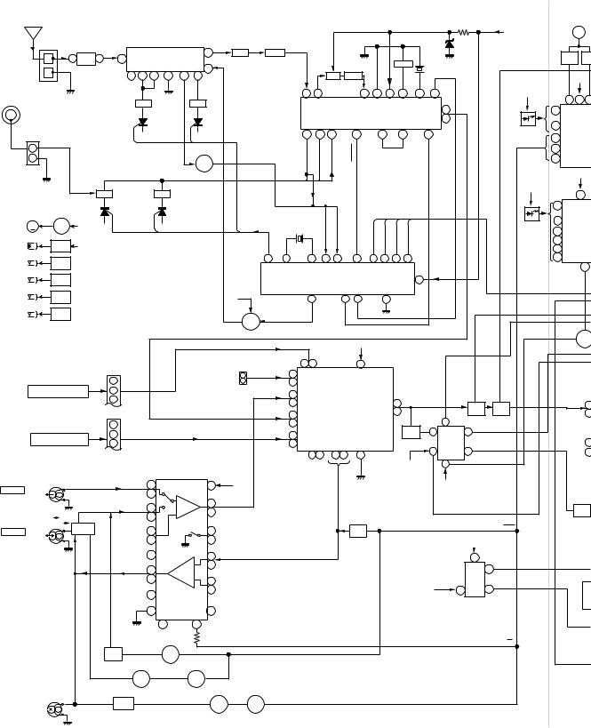
CD-K7000V,CP-C7000
FM
ANTENNA
+5V
+B4 |
M V |
|
M |
FM IF
|
|
1 |
BF301 |
3 |
1 |
|
|
|
IC301 |
|
6 |
|
T302 |
CF303 |
|
|
|
|
|
|
|
|
|
|
|
|
|
|
|
|
|
|
|
|
|
Q715 |
Q7 |
|
|
|
|
|
TA7358AP |
|
|
|
|
|
|
|
|
|
|
|
|
|
|
|
|
|
|
|
|
|
|
|
|
|
|
||||||||
|
|
B.P.F |
|
|
|
|
|
|
|
|
|
|
|
|
|
|
|
|
CF351 |
|
|
|
|
|
|
|
|
|
Q716 |
Q7 |
||||||||
|
|
|
|
|
|
|
FM FRONT END |
9 |
|
|
|
|
|
|
|
|
|
|
|
|
|
|
X351 |
|
|
|
|
|
|
|
|
|
||||||
|
|
|
|
|
|
2 |
3 |
4 |
5 |
7 |
8 |
|
|
|
|
|
|
|
T351 |
CF352 |
|
|
|
|
|
|
456kHz |
|
|
|
|
|
|
|
|
|||
|
|
|
|
|
|
|
|
|
|
|
|
|
|
|
|
|
|
|
|
|
|
|
|
|
|
|
+B6 |
|||||||||||
|
|
|
|
|
|
|
|
|
|
FM OSC |
|
|
|
|
|
|
|
|
AM IF |
|
|
|
|
|
|
|
|
|
|
|
|
|
|
|
|
|||
|
|
|
|
|
|
|
|
|
|
|
|
|
|
|
|
|
|
|
|
|
|
|
|
|
|
|
|
|
|
|
|
|
|
|
|
|||
AM LOOP |
|
|
|
|
|
|
|
|
|
|
|
|
|
|
1 |
|
2 |
|
|
|
4 |
5 |
9 |
|
|
8 |
17 |
13 |
|
|
|
|
|
|
+B4 |
16 18 1 |
||
ANTENNA |
|
|
|
|
FM RF |
L312 |
|
|
T301 |
|
|
|
|
|
AM MIX |
IC303 |
AM IF GND VCC FM |
VCO MO/ST |
|
|
|
|
|
|
||||||||||||||
|
|
|
|
|
|
|
|
|
|
|
|
|
|
|
|
|
|
DET |
|
L 14 |
|
|
|
|
5 |
|
|
|||||||||||
|
|
|
|
|
|
|
|
|
|
|
FM OSC |
|
|
|
|
|
|
|
LA1832S |
|
|
|
|
|
|
|
|
|
||||||||||
|
|
|
|
|
|
|
|
|
|
|
|
|
|
|
|
|
|
|
|
|
|
|
|
|
|
|
|
IC702 BU2902F INPUT/OUTPUT EXPANDER |
||||||||||
|
|
|
|
|
|
|
|
|
|
|
|
|
|
|
|
FM IF DET./FM MPX./AM IF |
|
|
|
|
|
R 15 |
|
|
|
|
~ |
|||||||||||
|
|
|
|
|
|
|
|
|
|
|
|
|
|
|
|
|
|
|
|
|
|
|
FM/AM |
|
|
|
|
|
|
|
|
11 |
||||||
|
|
|
|
|
|
|
|
|
|
|
|
|
|
|
|
|
|
|
|
|
|
|
OUT |
MPXIN |
FM/AM |
|
|
|
|
|
|
|||||||
|
|
|
|
|
|
|
|
|
|
|
|
|
|
|
|
24 |
|
23 |
|
21 |
|
7 |
|
18 |
|
16 |
|
12 |
|
|
|
|
|
|
12 |
|||
|
|
|
|
|
|
|
|
|
|
|
|
|
|
|
|
OSC OUT |
|
|
|
|
|
STEREO |
|
|
|
|
|
|
|
|
|
|
|
|
|
|||
|
1 |
|
|
|
|
|
|
|
|
|
OSC BUFF |
|
|
|
|
|
OSC IN |
RF IN |
|
|
|
|
|
|
|
|
|
|
|
|
|
|
13 |
|||||
|
|
|
|
|
|
|
|
|
|
|
|
|
|
|
|
|
|
|
|
|
|
|
|
|
|
|
|
|
|
|
||||||||
|
2 |
|
|
|
|
|
|
|
|
|
Q302 |
|
FM OSC |
|
|
|
|
|
|
|
|
|
|
|
|
|
|
|
|
14 |
||||||||
|
|
|
|
|
|
|
|
|
|
|
|
|
AM |
|
AM |
AM |
|
|
|
|
|
|
|
|
|
|
|
|
|
|
|
|
|
|||||
|
|
|
|
|
|
|
|
|
|
|
|
|
|
|
|
|
|
|
|
|
|
|
|
|
|
|
|
|
|
|
|
|
|
|||||
CNP301 |
|
|
|
|
|
|
|
|
|
|
|
|
|
|
|
|
|
|
|
|
|
|
|
|
|
|
|
|
|
|
|
|
|
|||||
|
|
|
|
|
|
|
|
|
|
|
|
|
|
|
|
|
|
|
|
|
|
|
|
|
|
|
|
|
|
|
|
|
|
|
+B6 |
|||
|
|
|
AM |
|
|
|
|
|
|
|
|
|
|
|
|
|
|
|
|
|
|
|
|
|
|
|
|
|
|
|
|
|
|
|
|
|
||
|
|
|
|
|
|
|
|
|
|
|
|
|
|
|
|
|
|
|
|
|
|
|
|
|
|
|
|
|
|
|
|
|
|
|
|
|
|
|
|
|
|
TRACKING |
|
|
|
|
|
AM BAND |
|
|
|
|
|
|
|
|
|
|
|
|
|
|
|
|
|
|
|
|
|
|
|
|
+B4 |
|
|
||
|
|
|
|
T303 |
|
|
T306 |
|
|
|
|
|
|
|
|
|
|
|
|
|
|
|
|
|
|
|
|
|
|
|
|
18 |
||||||
|
|
|
|
|
|
|
|
|
|
|
|
|
|
|
|
|
|
|
|
|
|
|
|
|
|
|
|
|
|
|
||||||||
|
|
|
|
|
|
COVERAGE |
|
|
|
|
|
|
|
|
|
|
|
|
|
|
|
|
|
|
|
|
|
|
|
|
|
|||||||
|
|
MOTOR |
|
|
|
|
|
|
|
|
|
|
|
|
|
|
|
|
|
|
|
|
|
|
|
|
|
|
|
|
|
|
|
|
|
5 |
|
|
|
|
|
|
|
|
|
|
|
|
|
|
|
|
|
|
|
|
|
|
|
|
|
|
|
|
|
|
|
|
|
|
|
|
|
~ |
|
EXPANDER |
|
|
|
DRIVER |
|
|
|
|
|
|
|
|
|
|
|
|
|
|
|
|
|
|
|
|
|
|
|
|
|
|
|
|
|
|
|
|
|
|
||
MM1 |
|
|
|
|
|
|
|
|
|
|
|
|
|
|
|
|
|
|
|
|
|
|
|
|
|
|
|
|
|
|
|
|
|
|
8 |
|
||
M |
Q708 |
+B3 |
|
|
|
|
|
|
|
|
|
|
|
|
X352 |
|
|
|
|
|
|
|
|
|
|
|
|
|
|
|
|
|
|
|
|
|||
TAPE |
|
|
|
|
|
|
|
|
|
VT |
|
|
|
|
|
|
|
|
|
|
|
|
|
|
|
|
|
|
|
|
10 |
|
||||||
MOTOR |
|
|
|
|
|
|
|
|
|
|
|
|
|
4.5MHZ |
|
|
|
|
|
|
|
|
|
|
|
|
|
|
|
|
|
|
|
|
||||
|
|
|
|
|
|
|
|
|
|
|
|
|
|
|
|
|
|
|
|
|
|
|
|
|
|
|
|
|
|
|
|
|
|
|
||||
SOLM1,SOLM2 |
|
Q704 |
+B3 |
|
|
|
|
|
|
|
|
|
|
|
|
|
|
|
|
|
|
|
|
|
|
|
|
|
|
|
|
|
|
|
|
11 |
|
|
SOLENOID |
|
Q705 |
|
|
|
|
|
|
|
|
|
|
|
|
|
|
|
AMIN |
|
FMIN |
|
CE |
DI |
CL |
|
DO |
|
|
|
|
|
|
|
|
13 |
IC703 BU2902F |
INPUT/OUTPUT L |
|
SWM2 |
|
IC701 |
|
|
|
|
|
|
|
|
|
|
|
20 |
1 |
22 |
15 |
16 |
|
11 |
3 |
4 |
5 |
|
6 |
|
|
|
|
|
|
|
|
16 |
|
5 |
||
T2 PLAY |
|
54PIN |
|
|
|
|
|
|
|
|
|
|
|
|
|
OSC |
|
IC302 |
|
|
|
|
|
|
|
|
|
|
|
|
|
|
|
|
|
|||
SWM1 |
|
IC701 |
|
|
|
|
|
|
|
|
|
|
|
|
|
|
|
|
|
|
|
|
|
|
|
|
|
|
|
|
|
|
|
|
|
|||
|
|
|
|
|
|
|
|
|
|
|
|
|
|
|
|
LC72131 |
|
|
|
|
|
|
VDD 17 |
|
|
|
|
|
|
|
|
|
|
|||||
T1 PLAY |
|
53PIN |
|
|
|
|
|
|
|
|
|
|
|
|
|
|
PLL(TUNER) |
|
|
|
|
|
|
|
|
|
|
|
|
|
|
|
|
|
||||
|
|
|
|
|
|
|
|
|
|
|
|
|
|
|
|
|
|
|
|
|
|
|
|
|
|
|
|
|
|
|
|
|
|
|||||
SWM4 |
|
IC701 |
|
|
|
|
|
|
|
|
|
|
|
|
|
|
|
|
|
FM/AM |
MO/ST |
|
|
|
|
|
|
|
|
|
|
|
|
|
|
|
|
|
|
|
|
|
|
|
|
|
|
|
+B4 |
|
|
|
7 |
|
|
|
9 |
10 |
|
21 |
|
|
|
|
|
|
|
|
|
|
|
|
|
|
|||
R. PLAY |
|
56PIN |
|
|
|
|
|
|
|
|
|
|
|
|
|
|
|
|
|
|
|
|
|
|
|
|
|
|
|
|
|
|
||||||
SWM3 |
|
IC701 |
|
|
|
|
|
|
|
|
|
|
|
|
|
|
|
|
|
|
|
|
|
|
|
|
|
|
|
|
|
|
|
|
|
|
|
|
F. PLAY |
|
55PIN |
|
|
|
|
|
|
|
|
|
FM +B |
FM |
|
|
|
|
|
|
|
|
|
|
|
|
|
|
|
|
|
|
|
|
|
|
|
|
|
|
|
|
|
|
|
|
|
|
|
|
|
|
Q360 |
|
|
|
|
|
|
|
|
|
|
|
|
|
|
|
|
|
|
|
|
|
|
|
|
|
|
|
|
|
|
|
|
|
|
|
|
|
|
SWITCHING |
|
|
|
|
|
|
|
|
|
|
|
|
|
|
|
|
|
|
|
|
|
|
|
Q401 |
|
|
|
|
|
|
|
|
|
|
|
|
|
|
|
|
|
|
|
|
|
|
|
+B4 |
|
|
|
|
|
|
|
|
|
|
|
|
|
|
|
|
|
|
|
|
|
|
|
|
|
|
|
|
|
|
|
|
|
|
|
|
|
|
|
|
|
|
|
|
|
|
|
|
|
|
|
|
|
|
|
|
|
|
|
|
|
|
|
|
|
|
|
|
|
|
|
L |
R |
|
|
|
|
|
|
|
|
|
|
|
|
|
|
|
|
|
|
|
|
|
|
|
|
|
|
|
|
|
|
|
|
|
|
|
|
|
7 17 |
|
|
|
23 |
|
|
|
|
|
|
|
|
|
|
|
|
|
|
|
|
||
|
|
|
|
|
1 |
|
|
|
|
|
JK601 |
L |
AUX |
L |
9 |
|
|
|
|
|
|
|
|
|
|
|
|
|
|
|
|
|
|
|
SYSTEM MUTE |
|
|
|
|
FROM MIC SECTION |
|
|
|
|
|
|
VIDEO IN R |
|
R 16 |
|
|
|
|
|
|
|
|
|
|
|
|
|
|
|
|
|
|
|
|
|
|||||||
|
|
2 |
|
|
|
|
|
|
|
|
|
L |
10 |
|
|
|
|
|
|
|
|
|
|
|
|
|
|
|
|
|
-20dB |
|
|
|||||
|
|
CNSK1 |
|
|
3 |
|
|
|
|
|
|
|
|
TAPE |
|
|
|
|
|
|
|
|
|
|
|
|
|
|
|
|
|
|
|
|||||
|
|
|
|
|
|
|
|
|
|
|
|
|
|
R 15 |
|
|
|
IC601 |
|
|
21 |
R |
|
|
|
|
|
|
ATT |
|
L |
5 |
||||||
|
|
|
|
|
|
|
|
|
|
|
|
|
|
|
|
|
|
|
|
|
|
|
|
|
Q603 |
|
Q605 |
|||||||||||
|
|
|
|
|
CNP601 |
|
|
|
|
|
|
|
|
|
|
|
|
|
|
LC75341 |
|
|
|
|
|
|
|
|
|
|
||||||||
|
|
|
|
|
|
|
|
|
|
|
|
|
TUNER |
L |
11 |
AUDIO PROCESSOR |
4 |
|
L |
|
|
|
|
|
|
Q604 |
|
Q606 |
|
6 |
||||||||
|
|
|
|
|
|
|
|
|
|
|
|
|
|
|
|
|
2 |
|
|
|
|
|
||||||||||||||||
|
|
|
|
|
1 |
|
|
|
|
|
|
|
|
|
R 14 |
|
|
|
|
|
|
|
|
|
|
Q862 |
1 |
|
OPE AMP. |
|
6 |
|
|
|
|
|||
|
|
|
|
|
2 |
|
|
|
|
|
|
|
|
|
L 12 |
|
|
|
|
|
|
|
|
|
|
|
KIA4558P |
|
|
|
|
|
||||||
|
FROM CD SECTION |
|
|
|
|
|
|
|
|
|
CD |
|
|
|
|
|
|
|
|
|
|
Q863 |
IC860 |
|
|
|
|
|
||||||||||
|
|
|
|
|
|
|
|
|
|
|
|
|
|
|
|
|
|
|
|
|
|
|
|
|
|
2 |
||||||||||||
|
|
CNP11 |
|
|
3 |
|
|
|
|
|
|
|
|
|
R 13 |
|
L |
|
R |
|
|
|
|
|
|
|
|
|
|
|
|
|
|
|||||
|
|
|
|
|
|
|
|
|
|
|
|
|
|
|
|
|
|
|
|
|
|
|
|
|
|
|
4 |
|
7 |
|
|
R |
||||||
|
|
|
|
|
CNS11 |
|
|
|
|
IC101 |
|
|
|
|
|
7 8 |
|
17 18 |
3 |
|
|
|
|
|
|
|
|
|
|
3 |
||||||||
|
|
|
|
|
|
|
|
|
AN7345K |
|
|
|
|
|
|
|
|
|
|
|
|
|
|
|
-B2 |
|
|
8 |
|
|
|
|
|
|
|
|
||
|
|
|
|
|
|
|
PLAYBACK AND RECORD |
|
|
|
|
|
|
|
|
|
|
|
|
|
|
|
|
|
|
|
|
|
|
|
|
|
|
|||||
|
|
|
|
|
|
|
|
|
/PLAYBACK AMP. |
|
|
|
|
|
|
|
|
|
|
|
|
|
|
|
|
|
|
|
|
|
|
|
|
|
|
|
||
TAPE 1 |
L-CH |
|
|
|
|
L(T1) |
1 |
|
|
VCC 13 |
|
+B4 |
|
|
|
|
|
|
|
|
|
|
|
|
|
|
|
|
+B4 |
|
|
|
|
|
|
|
||
|
|
|
|
R(T1) |
24 |
|
P.B |
|
|
|
|
|
|
|
|
|
|
|
|
|
|
|
|
|
|
|
|
|
|
|
|
|
|
|
||||
PB HEAD |
R-CH |
|
|
|
|
|
|
|
|
|
|
|
|
|
|
|
|
|
|
|
|
|
|
|
|
|
|
|
|
|
|
|
|
|||||
|
|
|
|
|
|
|
|
|
4 |
L |
|
|
|
|
|
|
|
|
|
|
|
|
|
|
|
|
|
|
|
|
|
|
|
|
|
|
||
|
|
|
|
|
|
L(T2) |
2 |
|
|
P.B |
|
|
|
|
|
|
|
|
|
|
|
|
|
|
|
|
|
|
|
|
|
|
|
Q864 |
||||
|
|
|
|
|
|
|
|
21 |
R |
|
|
|
|
|
|
|
|
|
|
|
|
|
|
|
|
|
|
|
|
|
|
|
|
|||||
|
|
REC |
|
|
|
R(T2) |
23 |
|
|
|
|
|
|
|
|
|
|
|
|
|
|
|
|
|
|
|
|
|
|
|
|
|
|
Q865 |
||||
|
|
SWITCHING |
|
|
|
|
|
|
|
|
|
|
|
|
|
|
|
|
|
|
|
|
|
|
|
|
|
|
|
|
|
|
||||||
|
|
P.B |
|
|
|
|
|
|
|
|
|
|
|
|
|
|
|
|
|
|
|
|
|
|
|
|
|
|
|
|
|
|
|
|
|
|||
|
|
Q103- |
|
|
|
|
|
|
|
|
|
|
|
|
|
|
|
|
|
|
Q121 |
|
|
|
|
|
|
|
|
|
|
|
|
|
REC |
|
|
|
|
|
|
|
|
L NF |
3 |
|
|
5 |
|
|
|
|
|
|
|
|
|
|
|
|
|
|
|
|
|
|
|
|
|
|
|
|
|
||||
TAPE 2 |
L-CH |
|
Q106 |
|
|
|
|
|
|
|
|
|
|
|
|
|
|
|
|
|
|
|
|
|
|
|
|
|
|
|
|
|
||||||
|
|
|
|
|
|
|
|
|
|
|
|
|
|
|
Q122 |
|
|
|
|
|
|
|
|
|
|
|
|
|
|
|
|
|||||||
REC PB HEAD R-CH |
|
|
|
|
R NF |
4 |
|
|
20 |
|
|
|
|
|
|
|
|
|
|
MUTING |
|
|
|
|
|
|
|
|
|
|
|
+B4 |
|
|
|
|
||
|
|
|
|
|
POP REDUCE |
6 T1/T2 |
|
H/N |
L |
|
|
|
|
|
|
|
|
|
|
|
|
|
|
|
|
|
|
|
|
|
|
|
|
|
|
|||
|
|
AC BIAS |
|
|
|
7 |
REC |
|
|
|
|
|
|
|
|
|
|
|
|
|
|
|
|
|
|
|
|
8 |
|
|
|
|
||||||
|
|
|
|
|
|
L REC |
9 REC |
|
18 |
R |
|
|
|
|
|
|
|
|
|
|
|
|
|
|
|
|
|
|
|
|
|
|
1 |
|
|
|
||
|
|
|
|
|
|
|
|
|
|
|
|
|
|
|
|
|
|
|
|
|
|
|
|
|
|
|
|
|
|
IC561 |
|
|
|
|||||
|
|
|
|
|
|
R REC |
16 |
|
|
|
|
|
|
|
|
|
|
|
|
|
|
|
|
|
|
|
|
|
|
|
|
|
|
|
|
|
||
|
|
|
|
|
|
|
|
8 L NF |
|
|
|
|
|
|
|
|
|
|
|
|
|
|
|
|
|
|
|
|
|
IC562 |
|
|
|
|
||||
|
|
|
|
|
|
REF |
14 |
|
|
17 R NF |
|
|
|
|
|
|
|
|
|
|
|
|
|
|
|
|
-B2 |
|
|
|
4 |
IC563 |
7 |
|
|
|
||
|
|
|
|
|
|
|
|
|
|
|
|
|
|
|
|
|
|
|
|
|
|
|
|
|
|
|
|
|
|
|
OPE |
|
|
|
|
|||
|
|
|
|
|
|
|
|
|
|
|
|
|
|
|
|
|
|
|
|
|
|
|
|
|
|
|
|
|
|
|
|
|
|
|
|
|
M |
|
|
|
|
|
|
|
|
|
12 |
NOR/ |
|
10 ALC |
|
|
|
|
|
|
|
|
|
|
|
|
|
|
|
|
|
|
|
|
|
AMP. |
|
|
|
|
|
|
|
|
|
|
|
|
|
|
HIGH |
|
T1/T2 |
|
|
|
|
|
|
|
|
|
|
|
|
|
|
|
|
|
|
|
|
|
KIA4558P |
|
|
|
||
|
|
|
|
|
|
|
|
|
15 |
|
19 |
|
|
|
|
|
|
|
|
|
|
|
|
|
|
|
|
|
|
|
|
|
|
|
|
|
|
|
|
|
|
|
|
|
|
|
|
SWITCHING |
|
|
|
|
|
|
|
|
|
|
|
|
|
|
|
|
|
|
|
|
|
|
|
|
T1/T2 |
|
|
||
|
|
|
|
|
Q107 |
|
|
|
Q111 |
|
|
|
|
|
|
|
|
|
|
|
|
|
|
|
|
|
|
|
|
|
|
|
|
|
|
|
|
|
|
|
|
|
|
Q108 |
|
|
|
|
|
|
|
|
|
|
|
|
|
|
|
|
|
|
|
|
|
|
|
|
|
|
|
|
|
|
|
||
|
|
|
|
|
|
|
|
|
|
|
|
|
|
|
|
|
|
|
|
|
|
|
|
|
|
|
|
|
|
|
|
|
|
|
|
|
|
|
|
|
|
|
SWITCHING |
|
|
|
|
|
|
|
|
|
|
|
|
|
|
|
|
|
|
|
|
|
|
|
|
|
|
|
|
|
|
|
|
||
|
|
|
|
|
|
|
Q109 |
SWITCHING Q110 |
|
|
|
|
|
|
|
|
|
|
|
|
|
|
|
|
|
|
|
|
|
|
|
|
|
|
|
|||
|
|
|
|
|
|
|
|
|
|
|
SWITCHING |
BIAS |
|
|
|
|
|
|
|
|
|
|
|
|
|
|
|
|
|
|
|
|
|
|
|
|
||
|
|
|
|
|
Q128 |
|
|
|
|
Q124 |
|
Q126 |
|
|
|
|
|
|
|
|
|
|
|
|
|
|
|
|
|
|
|
|
|
BIAS |
|
|
||
|
ERASE |
|
|
BIAS L104 |
|
|
|
|
|
|
|
|
|
|
|
|
|
|
|
|
|
|
|
|
|
|
|
|
|
|
|
|
|
|||||
|
|
|
|
|
|
|
|
|
|
|
|
|
|
|
|
|
|
|
|
|
|
|
|
|
|
|
|
|
|
|
|
|
|
|
||||
|
HEAD |
|
|
OSC |
|
|
|
|
|
|
|
|
|
|
|
|
|
|
|
|
|
|
|
|
|
|
|
|
|
|
|
|
|
|
|
|
|
|
Figure 18 BLOCK DIAGRAM (2/4)
– 18 –
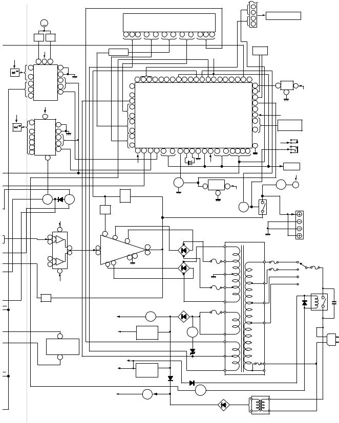
|
|
|
|
|
|
|
|
|
|
|
|
|
|
|
|
|
|
|
|
|
|
|
|
|
|
|
|
|
|
|
|
|
|
|
|
|
|
|
CD-K7000V,CP-C7000 |
||||
|
|
|
|
|
|
|
|
|
|
|
|
|
|
|
|
|
|
|
|
|
|
|
|
|
|
|
|
|
|
|
|
|
|
|
|
|
CNP601 |
|
|
|
|
|
|
|
|
|
|
|
|
|
|
|
|
|
|
|
|
|
|
|
|
|
|
|
|
|
|
|
|
|
|
|
|
|
|
|
|
|
|
|
|
8 |
|
|
|
|
|
|
|
|
|
|
|
|
|
|
|
|
|
|
|
|
|
|
|
|
|
|
|
|
|
|
|
|
|
|
|
|
|
|
|
|
|
|
|
9 |
FROM MIC SECTION |
|
|
|
|
|
|
|
|
M701 |
|
|
|
|
|
|
|
|
|
|
|
|
|
|
|
FL701 |
|
|
|
|
|
|
|
|
|
|
|
|
|
|
10 |
CNSK1 |
|
|
|
||||
|
|
|
|
|
|
|
|
|
|
|
|
|
|
|
|
|
|
|
|
|
|
|
|
|
|
|
|
|
|
|
|
|
|
|
|
|
|
|
|||||
+B4 |
|
M VOLUME |
|
|
|
|
|
|
|
|
|
|
|
|
|
|
|
DISPLAY |
|
|
|
|
|
|
|
|
|
|
|
|
|
11 |
|
|
|
|
|
||||||
|
|
|
MOTOR |
|
|
|
|
|
|
|
|
|
|
|
|
|
|
|
|
|
|
|
|
|
|
|
|
|
|
|
|
|
|
|
|
|
|
|
|
|
|
||
|
Q715 |
Q713 |
|
|
|
|
|
|
|
1 |
2 |
3 |
|
6 ~ 14 |
15 ~ 20 |
|
29 ~ 53 |
|
56 |
57 58 |
|
|
|
|
|
|
|
|
|
|
|
|
|||||||||||
|
Q716 |
Q714 |
|
|
|
|
|
|
|
|
|
|
|
|
|
|
|
|
|
|
|
|
|
|
|
|
|
|
|
|
|
|
|
|
|
|
|
|
|
|
|
||
|
|
+B6 |
|
|
|
|
|
|
|
Q701-Q703 |
|
|
|
|
|
|
|
|
|
|
|
|
|
|
|
|
|
|
|
|
|
|
|
|
|
JOG701 |
|
|
|
|
|
||
|
|
|
|
|
|
|
|
|
|
|
Q710-Q712 |
|
|
|
|
|
|
|
|
|
|
|
|
|
|
|
|
|
+B7 |
|
|
|
|
|
|
JOG |
|
|
|
|
|
||
+B4 |
|
|
|
|
|
|
|
|
|
|
|
|
|
|
|
|
|
|
|
|
|
|
|
|
|
|
|
|
|
|
|
|
|
|
|
|
|
|
|
|
|
||
16 18 15 |
|
|
|
|
|
|
|
|
|
|
|
|
|
|
|
|
|
|
|
|
|
|
|
|
|
|
|
|
|
|
|
|
|
|
|
|
|
|
|
||||
|
|
|
|
|
|
|
|
|
|
|
|
|
|
|
|
|
|
|
|
|
|
|
|
|
|
|
|
|
|
|
|
|
|
|
|
|
|
|
|
||||
5 |
|
BU2902F INPUT/OUTPUT EXPANDER |
|
17 |
|
|
|
|
|
|
|
|
|
|
|
|
|
|
|
|
|
|
|
|
|
|
|
|
|
|
|
|
|
|
|
|
|
RX701 |
|
|
|
||
~ |
|
|
1 |
|
|
|
|
|
|
|
|
|
|
|
|
|
|
|
|
|
|
|
|
|
|
|
|
|
|
|
|
|
|
|
|
|
|
|
|
||||
11 |
IC702 |
|
|
|
|
|
|
|
|
|
|
|
|
|
|
|
|
|
|
|
|
|
|
|
|
|
|
|
|
|
|
|
|
|
|
REMOCON |
|
|
|
||||
|
2 |
|
|
|
|
|
|
|
|
|
59 |
58 |
57 |
|
56 |
55 |
54 |
53 |
52 |
51 |
50 |
49 |
48 |
47 |
46 |
45 |
44 |
43 |
42 |
41 |
40 |
|
SENSOR |
|
|
|
|||||||
|
DI |
|
|
|
|
|
|
|
|
|
|
|
|
|
|
||||||||||||||||||||||||||||
12 |
|
|
|
|
|
|
|
|
|
|
|
|
|
|
|
|
|||||||||||||||||||||||||||
CL |
3 |
|
|
|
|
|
|
|
60 |
|
|
|
|
|
|
|
|
|
|
|
|
|
|
|
|
VDD |
|
|
|
|
|
|
39 |
1 |
3 |
|
|
|
|||||
13 |
|
|
|
|
|
|
|
|
|
|
|
|
|
|
|
|
|
|
|
|
|
|
|
|
|
|
|
|
|
|
|
|
|||||||||||
LCK 4 |
|
|
|
|
|
|
|
|
|
|
|
|
|
|
|
|
|
|
|
|
|
|
|
|
|
|
|
|
|
|
|
38 |
|
2 |
+B7 |
|
|
||||||
14 |
|
|
|
|
|
|
|
78 |
|
|
|
|
|
|
|
|
|
|
|
|
|
|
|
|
|
|
|
|
|
|
|
|
|
|
|||||||||
|
|
|
|
|
|
|
|
|
|
|
|
|
|
|
|
|
|
|
|
|
|
|
|
|
|
|
|
|
|
|
|
|
|
|
37 |
|
|
|
|
|
|||
|
|
|
|
|
|
|
|
|
|
|
|
|
79 VLOAD |
|
|
|
|
|
|
|
|
|
|
|
|
|
|
|
|
|
|
|
|
|
|
|
|
|
|
||||
|
|
|
|
|
|
|
|
|
|
|
|
|
|
|
|
|
|
|
|
|
|
|
|
|
|
|
|
|
|
|
SYS. STOP |
36 |
|
|
|
|
|
||||||
|
|
+B6 |
|
|
|
|
|
|
|
|
|
80 |
|
|
|
|
|
|
|
|
|
|
|
|
|
|
|
|
|
|
|
|
|
|
|
|
|
||||||
|
|
|
|
|
|
|
|
|
|
|
|
|
|
|
|
|
|
|
|
|
|
|
|
|
|
|
|
|
|
|
|
|
|
|
|
|
|
|
|
||||
|
|
|
|
|
|
|
|
|
|
|
|
|
|
|
|
|
|
|
|
|
|
|
|
|
|
|
|
|
|
|
|
|
|
|
|
35 |
|
|
|
|
|
||
+B4 |
|
|
|
|
|
|
|
|
|
|
|
|
~ |
|
|
|
|
|
|
|
|
|
|
IC701(1/2) |
|
|
|
|
|
|
|
|
|
|
|
|
|
|
|||||
|
|
|
|
|
|
|
|
|
|
|
|
|
|
|
|
|
|
|
|
|
|
|
|
|
|
|
|
|
|
|
|
|
|
|
|
|
|||||||
|
18 |
|
|
|
|
|
|
|
|
|
85 |
|
|
|
|
|
|
|
|
|
|
|
|
|
|
|
|
|
AVDD |
34 |
+B7 |
|
|
|
|||||||||
|
|
|
|
|
|
|
|
|
|
|
|
|
|
|
|
|
|
|
|
|
IX0360AW |
|
|
|
|
|
|
|
|
|
|
||||||||||||
|
|
|
|
|
|
|
|
|
|
|
|
|
|
|
|
|
|
|
|
|
|
|
|
|
|
|
|
|
|
|
|
|
|
|
|||||||||
5 |
|
|
INPUT/OUTPUT EXPANDER |
17 |
|
|
|
|
|
|
|
86 |
|
|
|
|
|
|
|
|
|
|
SYSTEM |
|
|
|
|
|
|
|
|
|
33 |
|
KEY |
|
|
|
|||||
~ |
|
|
|
|
|
|
|
|
|
~ |
|
|
|
|
|
|
|
|
MICROCOMPUTER |
|
|
|
|
|
|
|
~ |
SW701-SW719 |
|
|
|
||||||||||||
IC703 BU2902F |
|
|
|
|
|
|
|
|
|
|
|
|
|
|
|
|
|
|
|
|
|
|
|
|
SW723-SW734 |
|
|
|
|||||||||||||||
8 |
|
1 |
|
|
|
|
|
|
|
91 |
|
|
|
|
|
|
|
|
|
|
|
|
|
|
|
31 |
|
|
|
||||||||||||||
|
|
|
|
|
|
|
|
|
|
|
|
|
|
|
|
|
|
|
|
|
|
|
|
|
|
|
|
|
|
|
|
|
|
|
|
||||||||
10 |
DI |
2 |
|
|
|
|
|
|
|
92 |
|
|
|
|
|
|
|
|
|
RESET |
|
|
|
|
|
|
|
|
|
|
|
|
|
|
+B3 |
|
|
|
|
||||
11 |
CL |
3 |
|
|
|
|
|
|
|
~ |
VDD |
|
|
|
|
|
|
|
|
|
|
|
|
VDD |
|
|
|
|
|
|
|
|
|
|
|
|
|||||||
|
|
|
|
|
|
|
100 |
|
|
|
|
|
|
|
|
|
|
|
|
|
|
|
CE |
CL |
DI |
DO |
25 |
|
|
|
|
|
|||||||||||
13 |
|
|
|
|
|
|
|
|
|
|
|
|
|
|
|
|
|
|
|
|
|
|
|
|
|
|
|
|
|
||||||||||||||
|
|
LCK 4 |
|
|
|
|
|
|
|
|
|
1 |
2 |
4 |
5 |
7 ~ 9 |
10 11 12 13 |
15 16 |
17 ~ 20 |
21 24 23 24 |
|
|
|
|
|
|
|||||||||||||||||
16 |
|
|
|
|
|
|
|
|
|
|
|
|
|
|
|
|
JK670 |
|
|
|
|||||||||||||||||||||||
|
|
|
5 |
|
|
|
|
|
|
|
|
|
|
|
|
|
|
|
|
|
|
|
|
|
|
|
|
|
|
|
|
|
|
|
|
|
|
|
|
|
|
|
|
|
|
|
|
|
|
|
|
|
|
|
|
|
|
|
|
|
|
|
|
|
|
|
|
|
|
|
|
|
|
|
|
|
|
|
|
|
|
|
HEADPHONES |
|
|||
|
|
|
|
|
|
|
|
|
|
|
|
|
|
|
+B7 |
|
|
|
|
|
|
|
|
XL701 |
|
|
+B7 |
|
|
|
|
|
|
|
TO CD |
|
|
|
|||||
|
|
|
|
|
|
|
|
|
|
|
|
|
|
|
|
|
|
|
|
|
|
|
|
|
|
|
|
|
|
|
|
|
|
|
|
SECTION |
|
|
|
||||
|
|
|
|
|
|
|
|
|
|
|
|
|
|
|
|
|
|
|
|
|
|
|
|
|
4.1943MHz |
|
|
|
|
|
|
|
|
|
|
|
+B6 |
|
|
|
|||
|
|
|
|
|
|
|
|
|
|
|
|
|
|
|
|
|
|
|
|
|
|
|
|
|
|
|
|
|
|
|
|
|
|
|
|
|
|
|
|
|
|
|
|
|
|
|
|
|
|
|
|
|
|
|
|
|
|
|
|
|
|
|
|
|
|
|
|
|
|
|
|
|
|
|
|
|
|
|
|
|
|
|
DRIVER |
|
|
|
|
|
|
|
|
|
|
|
|
|
|
|
|
|
|
|
|
|
|
|
|
RESET |
Q709 |
|
|
|
|
IC704 |
|
|
|
|
|
|
Q907 |
M |
|
|
|
||||||
|
|
|
|
|
|
|
|
|
|
|
|
|
|
|
|
|
|
|
|
|
|
|
3 |
KIA7042P |
1 |
|
|
|
|
|
|
|
|
||||||||||
|
|
|
|
|
|
|
|
|
|
|
|
|
|
|
|
|
|
|
|
|
|
|
|
|
|
|
|
|
|
|
|
|
|
|
|
|
|||||||
|
|
|
|
|
|
|
|
|
|
|
|
Q901 |
|
|
|
|
|
|
|
|
|
|
|
|
|
|
|
|
|
RESET |
|
+B7 |
|
|
|
|
M901 |
|
|
|
|||
|
|
|
|
|
|
|
|
|
|
SP. DET. |
|
|
|
|
|
|
|
|
|
|
|
|
|
|
|
|
|
|
2 |
|
|
|
|
|
FAN MOTOR |
|
|
||||||
|
|
|
|
|
|
|
|
|
|
Q902 |
|
|
|
|
|
|
|
|
|
|
|
|
|
|
|
|
|
|
|
|
|
|
|
|
|
|
|
||||||
|
|
|
Q401 |
|
Q402 |
|
|
|
|
Q903 |
|
|
|
|
|
|
|
|
|
|
|
|
|
|
|
|
|
|
|
|
|
|
|
|
|
|
|
|
|
|
|
||
|
|
|
|
|
|
|
|
Q904 |
|
|
|
|
|
|
|
|
|
|
|
|
|
|
|
|
|
|
|
|
|
|
|
|
|
|
|
|
|
|
|
||||
|
|
|
|
|
|
|
|
|
|
|
|
|
|
|
|
|
|
|
|
|
|
|
|
|
|
|
|
|
|
|
|
|
|
|
|
|
|
RL901 |
|
|
|
|
|
|
|
|
|
|
|
|
|
|
|
Q910 |
|
|
|
|
|
|
|
|
|
|
|
|
|
|
|
|
|
|
|
|
|
|
|
|
|
Q905 |
|
|
|
|
|
||
|
|
|
|
|
|
|
|
|
|
Q911 |
|
|
|
|
|
|
|
|
|
|
|
|
|
|
|
|
|
|
|
|
|
|
|
|
|
|
|
|
|
|
|
|
|
|
|
|
|
|
|
|
|
|
|
|
|
|
|
|
|
|
|
|
|
|
|
|
|
|
|
|
|
|
|
|
|
|
|
|
|
|
|
|
|
|
|
|
|
|
|
|
|
|
+B4 |
|
|
|
|
|
|
|
|
|
|
|
|
|
|
|
|
|
|
|
|
|
|
|
|
|
|
|
|
|
|
|
|
|
|
|
L-CH |
|
|
MUTE |
|
|
|
|
8 |
|
|
|
|
|
|
|
|
|
|
|
|
|
|
|
|
|
|
|
|
-B2 |
|
|
|
|
|
|
|
|
|
|
|
|
|
|
|
|
|
|
|
|
|
|
|
|
|
13 |
|
|
|
|
|
|
|
|
|
|
|
|
|
|
|
|
|
|
|
|
|
|
|
|
|
|
|
|
|
|
R-CH |
|
|||
|
|
|
|
|
|
|
|
|
|
|
|
|
|
|
|
|
|
|
|
|
|
|
|
|
|
|
|
|
|
|
|
|
|
|
|
|
|
|
|
|
|||
5 |
|
L |
5 |
|
|
|
|
|
|
4 |
|
|
|
|
|
|
|
|
|
|
|
|
|
|
|
|
|
|
|
|
|
|
|
|
T801 |
|
|
|
|
|
|
||
|
|
|
|
|
|
|
|
|
|
|
|
|
|
|
|
|
|
|
|
|
|
|
|
|
|
|
|
|
|
|
|
|
|
|
|
|
|
||||||
6 |
|
|
6 |
IC401 KIA4558P OPE AMP. |
|
|
|
|
|
VL+ |
7 |
|
|
|
|
|
|
|
|
|
|
|
|
|
|
|
|
|
|
|
|
POWER TRANSFORMER |
|
SO901 |
|
|
|||||||
|
|
|
|
7 |
L |
R |
21 |
IC901 |
VL- |
|
|
|
|
14 R-OUT |
|
|
D809 |
|
|
|
|
|
|
|
|
|
|
|
|
|
|
|
SPEAKER |
|
|
||||||||
|
|
|
|
STK4115G |
|
|
|
|
|
|
|
|
|
|
|
|
|
|
|
|
|
|
|
|
|
|
|
|
TERMINAL |
|
|
||||||||||||
|
|
|
|
1 |
R |
L |
22 |
POWER AMP. |
|
|
|
|
15 |
L-OUT |
+B2 |
|
|
|
|
|
|
|
|
|
|
|
|
|
|
|
|
|
|
|
|
||||||||
|
|
|
|
|
|
|
|
12 |
|
|
|
|
|
|
|
|
|
|
|
|
|
|
|
|
|
|
|
F802 |
|
|
|
|
|||||||||||
|
|
|
2 |
|
VH- |
2 |
|
|
|
|
|
|
|
|
|
|
|
|
|
|
|
|
|
|
|
|
|
|
230-240V |
|
|
||||||||||||
|
|
|
|
|
|
|
|
|
VH+ |
|
|
|
|
|
|
|
|
|
|
|
|
|
|
|
|
|
|
|
|
|
|
|
|
|
T3.15A L 250V |
F801 |
|
||||||
|
|
|
|
|
|
|
|
|
|
|
|
|
|
|
|
|
|
|
|
|
|
|
|
|
|
|
|
|
|
|
|
|
|
|
|
||||||||
|
|
R 3 |
|
|
|
|
|
|
|
8 |
|
|
|
|
|
|
|
|
|
|
|
D810 |
|
|
|
|
|
|
|
|
|
|
|
|
|
|
|
|
|
|
|||
|
|
|
|
|
|
|
|
1 |
|
|
|
|
|
|
|
|
|
|
|
|
|
|
|
|
F804 |
|
|
|
|
|
|
|
|
220V |
|
T6.3A L 250V |
|||||||
|
|
|
|
|
4 |
|
|
|
|
+B1 |
|
|
|
|
|
|
|
|
|
|
|
|
|
|
|
|
|
|
T6.3A L 250V |
|
|
|
|
|
|
|
|
|
|||||
|
|
|
|
|
|
|
|
|
|
|
|
|
|
|
|
|
|
|
|
|
|
|
|
|
|
|
|
|
|
|
|
F803 |
|
|
|
|
|||||||
|
|
|
|
|
|
|
|
|
|
|
|
|
|
|
|
|
|
|
|
|
|
|
|
|
|
|
|
|
|
|
|
|
|
|
|
|
|
|
|
|
|
||
|
|
|
|
|
|
|
|
|
|
|
|
|
|
|
|
|
|
|
|
|
|
|
|
|
|
|
|
|
|
|
|
|
|
|
|
|
|
|
T3.15A L 250V 127V |
|
|
|
|
|
|
|
|
|
-B2 |
|
|
|
|
|
-B1 |
|
|
|
|
|
|
|
|
|
|
|
|
|
|
|
|
|
|
|
|
|
|
|
|
|
|
|
|
110V |
|
|
|
|
|
|
|
|
|
|
|
|
|
|
|
|
|
|
|
|
|
|
|
|
|
|
|
|
|
|
|
|
|
|
|
|
|
|
|
|
|
|
|
|
|
||
|
|
|
|
|
|
|
|
|
|
|
|
|
|
|
|
|
|
|
|
|
|
|
|
|
|
|
|
|
|
|
|
|
|
|
|
|
|
|
|
SW801 |
|
|
|
|
|
|
|
|
|
|
|
|
|
|
|
|
|
|
|
|
|
|
|
|
|
|
|
|
|
|
|
|
|
F805 |
|
|
|
|
|
|
|
VOLTAGE |
|
RL801 |
|
||
|
|
|
|
|
|
|
|
|
|
|
|
|
|
|
|
|
|
|
|
|
|
|
|
|
|
|
|
|
|
|
|
|
|
|
|
|
SELECTOR |
|
|
||||
|
|
Q864 |
|
|
|
|
|
|
|
|
|
|
|
|
|
|
|
|
|
|
|
|
|
|
|
|
|
T6.3A L 250V |
|
|
|
|
|
|
|
|
|
||||||
|
|
|
|
|
|
|
|
|
|
|
|
|
|
|
|
|
|
|
|
|
|
|
|
|
|
|
|
|
|
|
|
|
|
|
|
|
|
||||||
|
|
|
|
|
|
|
|
|
|
|
|
|
|
|
|
|
|
|
|
|
|
|
|
|
|
|
|
|
|
|
|
|
|
|
|
|
|
D801 |
|
C801 |
|||
|
|
Q865 |
|
|
|
|
|
|
|
|
|
|
|
|
|
|
|
|
|
|
|
|
|
|
|
|
|
|
|
|
|
|
|
|
|
|
|
|
|
||||
EC |
|
|
|
|
|
|
|
|
|
|
|
|
|
|
|
CONSTANT |
|
|
|
|
|
|
|
|
|
|
|
|
|
|
|
|
|
|
|
|
|
||||||
|
|
|
|
|
|
|
|
|
|
|
|
|
|
|
|
|
|
|
D811-D814 |
|
|
|
|
|
|
|
|
|
|
|
|
|
|
|
|
|
|||||||
|
|
|
|
|
|
|
|
|
|
|
|
|
|
|
VOLTAGE |
|
|
|
|
|
|
|
|
|
|
|
|
|
|
|
|
|
|
|
|
|
|||||||
|
|
|
|
|
|
|
|
|
|
|
|
|
|
|
|
|
|
|
|
|
|
|
|
|
|
|
|
|
|
|
|
|
|
|
|
|
|
|
|
||||
|
|
|
|
|
|
|
|
|
|
|
+B3 |
M10V |
|
|
|
Q850 |
|
|
|
|
|
|
|
|
|
|
F806 |
|
|
|
|
|
|
|
|
|
|
|
|||||
|
|
|
|
|
|
|
|
|
|
|
|
|
|
|
|
|
|
|
|
|
|
|
|
|
|
|
|
|
|
|
|
|
|
|
|
|
|||||||
|
|
|
|
|
|
|
|
|
|
|
|
|
|
|
|
|
|
|
|
|
|
|
|
|
|
|
|
|
|
T2A L 250V |
|
|
|
|
|
|
|
|
|
|
|
||
|
|
|
|
10Hz |
|
|
|
|
|
|
A10V |
|
|
Q851 |
|
|
|
|
|
|
|
|
|
|
|
|
|
|
|
|
|
|
|
|
|
|
|
|
|
AC POWER |
|||
|
|
|
|
|
|
|
|
|
+B4 |
|
KIA7810AP |
|
|
|
|
|
|
Q803 |
|
|
|
|
|
|
|
|
|
|
|
|
|
|
|
SUPPLY CORD |
|||||||||
|
|
|
|
|
|
|
|
|
|
|
|
|
|
|
|
|
|
|
|
|
|
|
|
|
|
|
|
|
|
|
|
|
|
|
|||||||||
|
|
|
|
|
27 |
|
|
|
|
|
|
|
|
|
|
VOLTAGE |
|
|
|
|
|
|
|
|
|
|
|
|
|
|
|
|
|
|
|
|
|
|
|
|
|||
|
|
|
|
|
|
|
|
|
|
|
|
|
|
REGULATOR |
|
|
|
|
|
|
|
|
|
|
|
|
|
|
|
|
|
|
|
|
|
|
|
|
|||||
|
|
|
|
IC701(2/2) |
|
|
VF2 |
|
|
|
|
|
|
|
|
|
|
|
|
|
|
|
|
|
|
|
|
|
|
|
|
|
|
|
|
|
|
|
|
|
|||
|
|
|
|
IX0360AW |
|
|
|
|
|
|
|
|
|
|
|
|
|
|
|
|
|
|
|
|
|
|
|
|
|
|
|
|
|
|
|
|
|
|
|
||||
|
|
|
|
|
|
|
|
|
|
|
|
|
|
|
|
|
|
|
|
|
|
|
|
|
|
|
|
|
|
|
|
|
|
|
|
|
|
|
|
AC 110/127/220 |
|||
|
|
|
|
SYSTEM |
|
|
|
|
|
|
|
VF1 |
|
|
|
|
|
|
|
|
|
|
|
|
|
|
|
|
|
|
|
|
|
|
|
|
|
|
|
||||
|
|
|
MICROCOMPUTER |
|
|
|
|
|
|
|
|
|
|
|
|
|
|
|
|
|
|
|
|
|
|
|
|
|
|
|
|
|
|
|
|
|
|
|
/230-240V |
||||
|
|
|
|
|
28 |
|
|
|
|
|
|
|
|
|
|
|
|
|
|
|
|
|
|
|
|
|
|
|
|
|
|
|
|
|
|
|
|
|
|
|
|
|
50/60Hz |
|
|
|
|
|
|
|
-VF |
|
|
|
+B6 |
|
|
+5V |
|
|
|
|
|
|
|
|
|
|
|
|
|
|
|
|
|
|
|
|
|
T.F |
|
|
|
|
|
||
|
|
|
|
|
|
|
|
|
|
|
|
|
|
|
|
|
|
|
|
|
|
|
|
|
|
|
|
|
|
|
|
|
|
|
|
|
|
|
|||||
|
|
|
|
|
|
|
|
|
|
|
|
|
|
|
|
|
|
|
|
|
|
|
|
|
|
|
|
|
|
|
|
|
|
|
|
|
|
|
|
|
|
||
|
|
|
|
63Hz |
|
|
|
|
|
+B5 |
CD+B |
|
|
Q852 |
|
|
|
|
|
|
|
|
|
|
|
|
|
|
|
|
|
|
|
|
|
|
|
|
|
|
|||
|
|
|
|
|
|
|
|
|
|
|
KIA7805P |
|
|
|
|
|
|
|
|
|
|
|
|
|
|
|
|
|
|
|
|
|
|
|
|
||||||||
|
|
|
|
|
|
|
|
|
|
|
|
|
|
|
|
|
|
|
|
|
|
|
|
|
|
|
|
|
|
|
|
|
|
|
|
|
|
|
|||||
/T2 |
|
|
|
|
|
|
|
|
|
|
|
|
|
|
|
VOLTAGE |
|
|
|
|
|
|
|
|
|
|
|
|
|
|
|
|
|
|
|
|
|
|
|
|
|||
|
|
|
|
|
|
|
|
|
|
|
|
|
|
REGULATOR |
|
|
|
|
|
|
|
|
|
|
|
|
|
|
|
|
|
|
|
|
|
|
|
|
|||||
|
|
|
|
|
|
|
|
|
|
|
|
|
|
|
|
|
|
|
|
|
|
|
|
|
|
|
|
|
|
|
|
|
|
|
|
|
|
|
|||||
|
|
|
|
|
|
|
|
|
|
|
|
|
|
|
|
|
|
|
|
|
|
|
|
|
|
|
Q802 |
|
|
|
|
|
|
|
|
|
|
|
|
|
|
||
|
|
|
|
|
|
|
|
|
|
+B7 |
|
|
|
|
Q801 |
|
|
|
|
|
|
|
|
|
|
|
|
|
|
|
|
|
|
|
|
|
|
|
|
|
|||
|
|
|
|
|
|
|
|
|
|
UNSWITCH 5V |
|
|
CONSTANT |
|
|
|
|
|
|
|
|
|
|
|
|
|
|
|
|
|
|
|
|
|
|
|
|
||||||
|
|
|
|
|
|
|
|
|
|
|
|
|
|
|
|
|
|
|
|
|
|
|
|
|
|
|
|
|
|
|
|
|
|
|
|
|
|
|
|||||
|
|
|
|
|
|
|
|
|
|
|
|
|
|
|
|
VOLTAGE |
|
|
|
|
|
|
|
|
|
|
|
|
|
|
|
|
|
|
|
|
|
|
|
|
|||
AS |
|
|
|
|
|
|
|
|
|
|
|
|
|
|
REGULATOR |
|
|
|
|
|
|
|
|
|
|
|
|
|
|
|
|
|
|
|
|
|
|
|
|
||||
|
|
|
|
|
|
|
|
|
|
|
|
|
|
|
|
|
|
|
|
|
|
|
|
|
|
|
|
|
|
|
D802-D805 |
|
|
|
T802 |
|
|
|
|
|
|||
|
|
|
|
|
|
|
|
|
|
|
|
|
|
|
|
|
|
|
|
|
|
|
|
|
|
|
|
|
|
|
|
|
|
|
|
|
|
|
|
|
|
|
|
|
|
|
|
|
|
|
|
|
|
|
|
|
|
|
|
|
|
|
|
|
|
|
|
|
|
|
|
|
|
|
|
|
|
|
|
|
|
POWER |
|
|
|
|
|
|
|
|
|
|
|
|
|
|
|
|
|
|
|
|
|
|
|
|
|
|
|
|
|
|
|
|
|
|
|
|
|
|
|
|
|
|
TRANSFORMER |
|
|
|
|
||
Figure 19 BLOCK DIAGRAM (3/4)
– 19 –
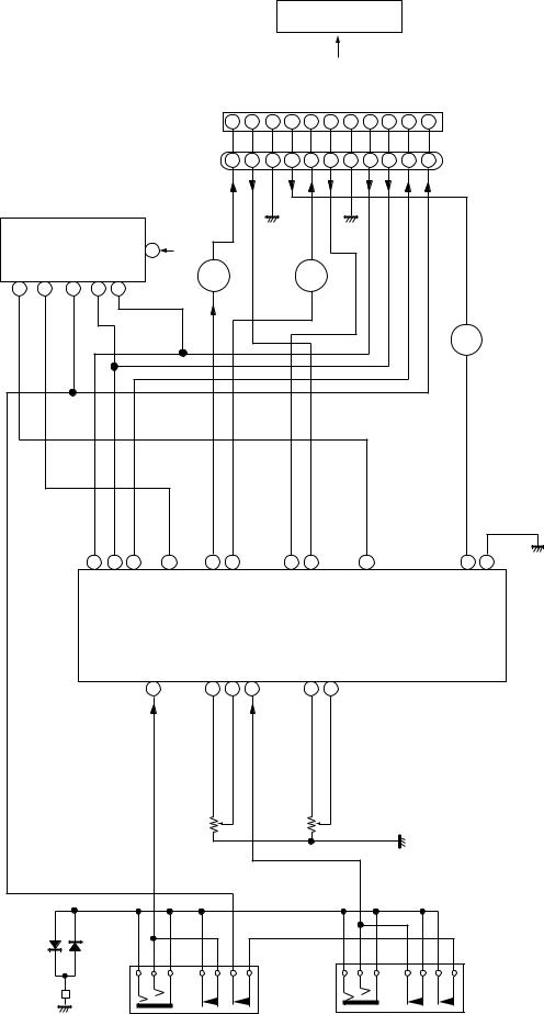
CD-K7000V,CP-C7000
TO MAIN SECTION
(TO IC601)
|
|
|
|
|
|
|
|
|
OUT(L) |
IN(L) |
GND(A) |
+10V(+B4) |
OUT(R) |
IN(R) |
GND(D) |
DATA |
CLOCK |
LATCH |
MIC IN |
|
|
|
|
|
|
|
|
|
|
|
1 |
2 |
3 |
4 |
5 |
6 |
7 |
8 |
9 |
10 |
11 |
CNSK1 |
|
|
|
|
|
|
|
|
|
|
1 |
2 |
3 |
4 |
5 |
6 |
7 |
8 |
9 |
10 |
11 |
BIK1 |
|
|
|
ICK2 |
|
|
|
|
|
|
|
|
|
|
|
|
|
|
|
|
|
|
|
|
M65847AFP1 |
|
|
|
|
|
|
|
|
|
|
|
|
|
|
|
|
|
|
||
KEY CONTROL |
|
|
|
|
|
|
|
|
|
|
|
|
|
|
|
|
|
||||
MIXOUT |
LPF1N |
STROBE |
SCK |
SDATA |
VCC |
14 |
|
+B4 |
|
|
|
|
|
|
|
|
|
|
|
|
|
|
|
QK3 |
|
|
|
QK2 |
|
|
|
|
|
|
|
|
|||||||
15 |
22 |
9 |
8 |
7 |
|
|
|
|
|
|
|
|
|
|
|
|
|
|
|||
|
|
|
|
|
|
|
|
|
|
|
|
|
|
|
|
|
|||||
|
|
|
|
|
|
|
|
|
|
|
|
|
|
|
|
|
|
|
|
QK1 |
|
|
|
|
42 |
41 |
40 |
|
40 |
36 |
35 |
|
|
32 |
31 |
|
|
15 |
|
|
|
23 |
22 |
|
ICK1 |
M65856SP MIC AMP. |
DATA |
CLDCK |
LATCH |
|
SOURCE OUT |
MICLOUT LOUT |
ROUT |
|
|
RIN |
LIN |
MIC2VOLIN |
|
KEYCON IN |
|
|
|
VCC |
GND |
|
MIC1IN |
MIC1VOLIN |
MIC2IN |
|
MIC2OUT |
|
|
|
|
||||||||||||
|
|
|
|
|
|
4 |
|
7 |
8 |
9 |
|
|
12 |
13 |
|
|
|
|
|
|
|
|
|
|
|
|
|
|
|
|
|
|
|
|
|
|
VRK1 |
|
|
|
|
|
|
|
|
|
|
|
|
|
VRK2 |
|
|
|
|
|
|
MIC1 |
|
|
|
|
|
||
|
|
|
|
|
|
|
MIC2 |
|
|
|
|
|
|
VOLUME |
|
|
|
|
|||
|
|
|
|
|
|
VOLUME |
|
|
|
|
|
|
|
|
|
|
|
|
|
||
PINK1 |
|
|
|
|
|
|
|
|
|
|
|
|
|
|
|
|
|
|
|
||
|
CHASSIS |
|
|
|
|
JK2 |
|
|
|
|
|
|
|
|
JK1 |
|
|
|
|||
|
|
GND |
|
|
|
|
|
MIC2 |
|
|
|
|
|
|
|
|
MIC1 |
|
|
|
|
Figure 20 BLOCK DIAGRAM (4/4)
– 20 –
CD-K7000V,CP-C7000
A
B
C
D
E
F
G
P27 12 - F
TO MAIN PWB
CNP601
1 2 3 4 5 6 7 8 9 10 11 CNSK1
OUT(L) |
IN(L) |
GND(A) |
+10V(A) |
OUT(R) |
IN(R) |
GND(D) |
DATA |
CLOCK |
LATCH |
MIC IN |
|
|
|
|
|
|
|
|
|
|
|
|
|
KARAOKE PWB-D
 MIC SIGNAL
|
|
|
|
|
|
|
|
|
|
|
|
|
|
CK69 |
|
|
|
|
|
|
|
|
|
|
|
||
|
|
|
|
|
|
|
|
|
|
|
|
|
|
2.2/50 |
|
|
|
|
|
|
|
|
|
|
|
||
|
|
10K |
|
|
|
|
|
|
RK34 |
RK32 10K |
RK31 10K |
|
CK66 |
CK64 0.01 |
10K |
10K |
|
4.7K |
|
CK61 |
2.2/50 |
||||||
|
|
|
|
|
|
|
|
CK65 |
0.01 |
CK67 |
0.01 |
0.01 |
RK28 |
RK27 |
|
RK25 |
|
|
|
||||||||
|
|
RK35 |
CK71 |
0.047(ML) |
CK70 |
0.047 |
(ML) |
CK68 0.0047 |
RK33 10K |
RK30 |
5.6K |
|
RK29 10K CK63 |
470P CK62 |
470P |
RK26 |
.7K4 RK23 |
4.7K |
CK60 |
0.0015(ML) |
|||||||
ICK2 M65847AFP1 CONTROLKEY |
|
|
|
|
|
|
|
|
|
10K |
|
|
|
|
|
|
|
|
|
|
|
|
|
|
|
|
|
ADCONT MODE2 |
DA1CONT |
MODE1 |
DA2CONT |
DA1NTOUT |
KEYDOWN DA1NTIN |
KEYUP |
ADINTOUT |
CLKO |
|
SDATA |
|
SCK |
|
STROBE |
|
HPFOUT |
LPF2IN |
REF |
GND |
Vcc |
|
|
|||||
|
28 |
27 |
26 |
|
25 |
24 |
23 |
22 |
|
21 |
|
20 |
|
19 |
18 |
17 |
16 |
15 |
|
|
|||||||
|
|
|
|
|
|
|
|
|
|
ADINTIN |
|
LPF1IN |
|
|
LPF1OUT |
|
|
HPFIN |
|
|
|
|
LPF2OUT |
MIXIN |
MIXOUT |
|
|
|
1 |
2 |
|
3 |
|
4 |
5 |
6 |
|
7 |
|
8 |
|
9 |
|
10 |
11 |
12 |
13 |
14 |
|
|
|||||
CK50 |
0.068(ML) |
CK51 |
0.068(ML) |
|
|
CK52 |
0.068(ML) |
|
|
CK53 |
47P |
|
CK5447P |
|
|
|
RK20 |
1K |
47/25 |
|
|
|
|
||||
|
|
|
|
|
|
|
|
CK55 |
47P |
|
CK56 |
|
|
|
|
||||||||||||
|
|
|
|
|
|
|
|
|
|
|
|
|
|
|
|
|
|
RK21 |
1K |
|
|
|
|
|
|||
|
|
|
|
|
|
|
|
|
|
|
|
|
|
|
|
|
|
RK22 |
1K |
|
|
|
|
|
|||
|
|
|
|
|
|
|
|
|
|
|
|
|
|
|
|
|
|
|
|
|
|
|
|
CK57 |
|
|
|
|
|
|
|
|
|
|
|
|
|
|
|
|
|
|
|
|
|
|
|
|
|
|
|
100/16 |
|
||
|
|
|
|
|
|
|
|
|
|
|
|
|
|
|
|
|
|
|
|
|
|
|
|
|
CK58 |
|
|
|
|
|
|
|
|
|
|
|
|
|
|
|
|
|
|
|
|
|
|
|
|
|
|
|
0.022 |
|
|
1 |
2 |
3 |
4 |
5 |
6 |
7 |
8 |
9 |
10 |
11 |
BIK1 |
|
||||
|
|
|
|
|
|
|
|
|
|
|
|
|
|
|
||
RK39 |
1K |
|
|
+B |
|
|
RK40 |
|
|
|
|
|
|
+B |
|
|
|
|
|
|
|
|
1K |
|
|
|
|
|
|
|
|||
|
RK37 |
1K |
|
RK36 |
|
|
|
|
|
|
|
|
|
|
|
|
|
|
|
|
1K |
|
|
|
|
|
|
|
|
|
|
|
|
|
|
|
CK73 |
2.2/50 |
|
|
|
|
|
|
|
|
|
|
RK47 |
|
|
|
|
|
|
|
|
|
|
|
|
|
|
|
|
||
|
|
|
|
|
|
|
|
|
|
|
|
|
|
|
680 |
|
|
RK41 |
1.5K |
|
RK43 |
470K |
RK45 |
1K |
QK3 |
KTC3199GR |
|
|
|
|
RK38 |
CK72 100/16 |
|
|
|
|
|
|
|
|
|
|
|
|
|
|
|
|
100 |
|
|
|
|
|
RK42 |
1.5K |
CK74 |
2.2/50 |
|
|
|
|
RK14 |
|
RK15 |
|
|
|
|
|
|
RK48 |
|
|
|
100 |
100 |
|||||||
|
RK44 |
470K |
RK46 1K |
QK2 |
680 |
|
|
|
|
|
|
|
|
|||
|
KTC3199GR |
|
|
|
|
|
|
|
|
ZDK1 |
||||||
|
|
|
|
|
|
|
|
|
|
|
|
|
|
|
CK44 |
|
|
|
|
|
|
|
|
|
|
|
|
|
|
|
|
47/25 |
|
|
|
|
|
|
|
|
|
|
|
|
|
|
+B |
|
|
|
|
|
|
|
|
|
|
|
|
|
|
|
|
|
KTC3203Y |
MTZJ5.6B |
|
|
|
|
|
|
|
|
|
|
|
|
|
|
QK1 |
RK13 1.2K |
RK12 100 |
|
|
|
|
|
|
|
|
|
|
|
|
|
|
|
|
|
CK43 |
|
|
|
|
|
|
|
|
|
|
|
|
|
|
|
|
47/25 |
HEADPHONES PWB-A3
FM SIGNAL
|
JK670 |
|
|
|
HEADPHONES |
|
|||
1 |
2 |
3 |
4 |
WT601 |
5 |
||||
|
FW902 |
|
||
|
P33 12 - D |
|
||
|
TO POWER |
|
||
|
AMP. PWB |
|
||
|
|
|
|
|
|
|
|
|
|
|
|
|
|
|
|
|
|
|
|
|
|
|
|
|
|
CK42 |
|
|
|
|
|
|
|
|
|
|
|
|
|
|
|
|
|
|
|
|
|
|
|
|
|
|
0.022 |
+B |
|
|
|
|
|
|
|
|
|
|
|
|
|
|
|
|
|
|
|
|
|
|
|
+B |
|
|
|
|
|
|
|
|
|
|
|
|
|
|
|
|
|
|
|
|
|
|
|
|
|
|
CK41 |
||
|
|
|
|
|
|
|
|
|
|
|
|
|
|
|
|
|
|
|
|
|
|
|
|
|
|
|
|
|
|
|
|
|
|
|
|
|
|
|
|
|
|
|
|
|
|
|
|
|
|
|
|
|
47/25 |
CK35 |
47P |
|
|
|
|
CK34 |
47P |
CK33 |
47P |
0.15 |
2.2/50 |
2.2/50 |
2.2/50 |
2.2/50 |
2.2/50 |
2.2/50 |
2.2/50 |
|
0.001 |
0.0047 |
|
|
|
0.22 |
+B |
CK19 |
|
|
|
|
|
|
|
|
|
|
|
|
|
|
|
|
|
|
|
|
|
|
|
|
|
|
0.022 |
|
|
RK11 |
1K |
RK101K |
|
|
RK9 1K |
|
|
CK31 |
CK29 |
CK30 |
CK28 |
CK27 |
CK26 |
CK25 |
CK24 |
|
CK23 |
CK22 |
|
CK21 0.068(ML) |
|
CK20 |
|
CK18 |
|
|
|
|
|
|
|
|
|
|
|
|
|
|
|
|
|
|
|
|
|
|
|
|
|
|
100/16 |
|
|
|
42 |
41 |
40 |
39 |
38 |
37 |
36 |
35 |
34 |
33 |
32 |
31 |
30 |
29 |
28 |
27 |
26 |
25 |
24 |
23 |
22 |
|||
ICK1 |
M65856SP MIC AMP. |
MICSW DATA |
MCLKCONT CLOCK |
VALC LATCH |
MIC1IN PS2 |
ALC1 PS1 |
MIC1NFIN VCFIL |
MIC1OUT LOUT |
MIC1VOLIN ROUT |
MIC2IN SOURCEOUT |
ALC2 KEYCONIN |
MIC2NFIN RIN |
MIC2OUT LIN |
MIC2VOLIN VOLIN |
MICOUT LPF2OUT |
LPF1IN1 LPF2IN2 |
LPF2IN2 LPF2IN1 |
LPF1OUT DAINTOUT |
ADINTOUT DAINTIN |
ADINTIN DACONT |
ADCONT VCC |
REF GND |
||||
|
|
|
1 |
2 |
3 |
4 |
5 |
6 |
7 |
8 |
9 |
10 |
11 |
12 |
13 |
14 |
15 |
16 |
17 |
18 |
19 |
20 |
21 |
|||
|
|
CK1 0.01 |
|
RK4 |
10K |
RK5 1K |
RK6 |
VOLUME |
RK7 1K CK8 4.7/50 |
VRK1 20K(B) |
CK11 0.1 |
MIC1 VOLUME |
|
CK13 |
0.0047 |
|
CK15 0.068(ML) |
CK16 0.22 |
CK17 220/10 |
|||||||
|
RK1 |
|
|
|
|
0.47 |
4.7/50 |
2.2/50 |
0.1 |
0.1 |
0.47 |
|
2.2/50 |
0.1 |
|
2.2/50 |
|
CK14 |
0.001 |
|
|
|
|
|||
|
10K |
|
|
|
|
|
|
|
|
|
|
|
|
|
|
|
|
|
|
|
|
|
|
|
|
|
|
RK2 |
|
|
|
|
CK2 |
CK3 |
CK4 |
CK5 |
CK6 |
CK7 |
|
CK9 |
CK10 |
|
CK12 |
|
|
|
|
|
|
|
|
||
|
56K |
|
|
|
|
|
|
|
VRK2 20K(B) |
|
|
|
|
|
|
|
|
|
|
|
|
|
|
|
||
56K |
|
|
|
|
|
|
|
|
|
|
|
|
|
|
|
|
|
|
|
|
|
|
|
|||
+B |
|
|
|
|
|
|
|
|
|
|
|
|
|
|
|
|
|
|
|
|
|
|
|
|
|
|
RK3 |
|
|
|
|
|
|
|
|
|
|
|
|
|
|
|
|
|
|
|
|
|
|
|
|
|
|
|
|
|
|
|
|
|
|
|
|
|
MIC2 |
|
|
|
|
|
|
|
|
|
|
|
|
|
|
|
|
|
|
|
|
|
|
|
|
5.6K |
|
|
|
|
|
|
|
|
|
|
|
|
|
|
|
|
|
|
|
|
|
|
|
|
|
|
|
|
|
|
|
|
|
RK8 |
|
|
|
|
|
|
|
|
|
|
|
|
|
|
|
|
|
|
|
|
|
|
|
|
|
|
5.6K |
|
|
|
|
|
|
|
|
|
|
DK1 1SS133 |
|
|
DK2 |
1SS133 |
|
|
|
|
|
|
|
|
|
|
|
|
|
|
|
|
|
|
|
|
|
|
PINK1 |
|
|
H |
JK2 |
JK1 |
CHASSIS |
||
GND |
MIC2 |
MIC1 |
• NOTES ON SCHEMATIC DIAGRAM can be found on page 16.
|
1 |
2 |
3 |
4 |
5 |
6 |
Figure 21 SCHEMATIC DIAGRAM (1/13)
– 21 –
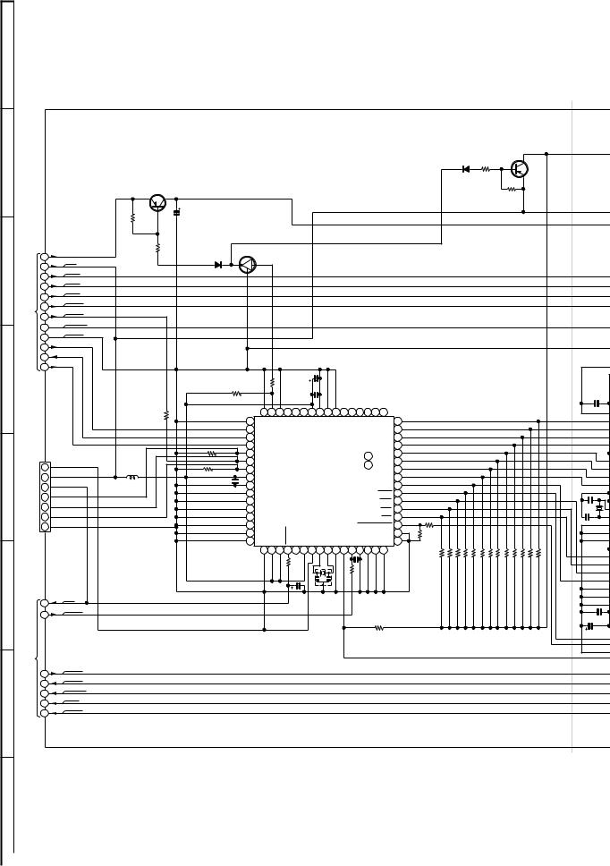
CD-K7000V,CP-C7000
A
|
|
|
|
|
|
|
|
|
|
|
|
|
|
|
|
|
|
|
|
|
|
|
|
|
|
|
|
|
|
DV5 |
|
|
QV4 |
|
+B |
|
|
|||
|
|
|
|
|
|
|
|
|
|
|
|
|
|
|
|
|
|
|
|
|
|
|
|
|
|
|
|
|
|
|
KTA1298 Y |
|
|
|
||||||
B |
|
|
|
|
|
|
|
|
|
|
|
|
|
|
|
|
|
|
|
|
|
|
|
|
|
|
|
|
KDS193 |
|
|
|
||||||||
|
|
|
|
|
|
|
|
|
|
|
|
|
|
|
|
|
|
|
|
|
|
|
|
|
|
|
|
|
|
|
|
|
|
|
|
|||||
|
|
|
|
|
|
|
|
|
|
|
|
|
|
|
|
|
|
|
|
|
|
|
|
|
|
|
|
|
|
|
|
|
|
|
|
|
|
|
|
|
|
|
|
|
|
|
|
|
|
|
|
|
|
|
|
|
|
|
|
|
|
|
|
|
|
|
|
|
|
|
|
|
RV84 |
|
|
|
|
|
|
||
|
|
|
|
QV2 |
|
|
|
|
|
|
|
|
|
|
|
|
|
|
|
|
|
|
|
|
|
|
|
|
|
|
4.7K |
|
|
|
|
|
|
|||
|
|
|
|
|
|
|
|
|
|
|
|
|
|
|
|
|
|
|
|
|
|
|
|
|
|
|
|
|
|
|
|
|
|
|
|
|
|
|
||
|
|
|
|
KTA1298 Y |
|
|
|
|
|
|
+B |
|
|
|
|
|
|
|
|
|
|
|
|
|
|
|
|
|
|
|
|
|
|
RV85 |
|
|
|
|||
|
|
|
|
|
|
|
|
|
|
|
|
|
|
|
|
|
|
|
|
|
|
|
|
|
|
|
|
|
|
|
|
|
|
|
|
|
||||
|
|
|
|
|
|
|
|
|
|
|
|
|
|
|
|
|
|
|
|
|
|
|
|
|
|
|
|
|
|
|
|
|
|
|
|
10K |
|
|
|
|
|
|
|
|
RV1 |
|
CV1 |
|
|
|
|
|
|
|
|
|
+B |
|
|
|
|
|
|
|
|
|
|
|
|
|
|
|
|
|
|
|
|
|
|
|
|
|
|
|
|
|
47/6.3 |
|
|
|
|
|
|
|
|
|
|
|
|
|
|
|
|
|
|
|
|
|
|
|
|
|
|
|
|
|
|
+B |
|
|
||
|
|
|
|
10K |
|
|
|
|
|
|
|
|
|
|
|
|
|
|
|
|
|
|
|
|
|
|
|
|
|
|
|
|
|
|
|
|
|
|
|
+B |
|
|
|
|
|
|
|
|
|
|
|
|
+B |
|
|
|
|
|
|
|
|
|
|
|
|
|
|
|
|
|
|
|
|
|
|
|
|
|
|
|
|
|
|
|
|
|
RV2 |
|
|
|
QV3 |
|
|
|
|
|
|
|
|
|
|
|
|
|
|
|
|
|
|
|
|
|
|
|
|
|
|
|
|
|
|
|
|
|
10 |
3.3V |
+B |
1K |
|
DV4 |
|
KRC104 S |
|
|
|
|
|
|
|
|
|
|
|
|
|
|
|
|
|
|
|
|
|
|
|
|
|
|
|
|
|
||
|
|
+5V |
|
|
KDS193 |
2 |
3 |
|
|
|
|
|
|
|
|
|
|
|
|
|
|
|
|
|
|
|
|
|
|
|
|
|
|
|
|
|
|
|
||
|
|
|
|
|
|
|
|
|
|
|
|
|
|
|
|
|
|
|
|
|
|
|
|
|
|
|
|
|
|
|
|
|
|
|
|
|||||
C |
|
8 |
C2PO |
+B |
|
|
|
|
1 |
|
|
|
|
|
|
|
|
|
|
|
|
|
|
|
|
|
|
|
|
|
|
|
|
|
|
|
|
|
|
|
|
18 |
|
|
|
|
|
|
|
|
|
|
|
|
|
|
|
|
|
|
|
|
|
|
|
|
|
|
|
|
|
|
|
|
|
|
|
||||
|
|
4 |
LRCK |
|
|
|
|
|
|
|
|
|
|
|
|
|
|
|
|
|
|
|
|
|
|
|
|
|
|
|
|
|
|
|
|
|
|
|
|
|
|
|
BCLK |
|
|
|
|
|
|
|
|
|
|
|
|
|
|
|
|
|
|
|
|
|
|
|
|
|
|
|
|
|
|
|
|
|
|
|
|
|
|
|
SECTION -12C,- D |
|
|
|
|
|
|
|
|
|
|
|
|
|
|
|
|
|
|
|
|
|
|
|
|
|
|
|
|
|
|
|
|
|
|
|
|
|
|
|
|
3 |
DATAD |
|
|
|
|
|
|
|
|
|
|
|
|
|
|
|
|
|
|
|
|
|
|
|
|
|
|
|
|
|
|
|
|
|
|
|
|
|
|
|
|
|
|
|
|
|
|
|
|
|
|
|
|
|
|
|
|
|
|
|
|
|
|
|
|
|
|
|
|
|
|
|
|
|
|
|
|
|
||
|
|
2 |
|
|
|
|
|
|
|
|
|
|
|
|
|
|
|
|
|
|
|
|
|
|
|
|
|
|
|
|
|
|
|
|
|
|
|
|
|
|
|
|
MBUSY |
|
|
|
|
|
|
|
|
|
|
|
|
|
|
|
|
|
|
|
|
|
|
|
|
|
|
|
|
|
|
|
|
|
|
|
|
|
|
|
|
|
|
|
|
|
|
|
|
|
|
|
|
|
|
|
|
|
|
|
|
|
|
|
|
|
|
|
|
|
|
|
|
|
|
|
|
|
|
|
|
CD 12 |
16 |
AV_GND |
|
|
|
|
|
|
|
|
|
|
|
|
|
|
|
|
|
|
|
|
|
|
|
|
|
|
|
|
|
|
|
|
|
|
|
|
|
|
11 |
|
|
|
|
|
|
|
|
|
|
|
|
|
|
|
|
|
|
|
|
|
|
|
|
|
|
|
|
|
|
|
|
|
|
|
|
|
||
|
TO P25 |
D_GND |
|
|
|
|
|
|
|
|
|
|
|
|
|
|
|
|
|
|
|
|
|
|
|
|
|
|
|
|
|
|
|
|
|
|
|
|
|
|
|
12 |
+B |
|
|
|
|
|
|
|
|
|
|
|
|
|
|
|
|
|
|
|
|
|
|
|
|
|
|
|
|
|
|
|
|
|
|
|
|
||
|
|
|
|
|
|
|
|
|
|
|
|
|
|
|
+B |
|
|
|
|
|
|
|
|
|
|
|
|
|
|
|
|
|
|
|
|
|
|
|
||
|
|
MDI |
|
|
|
|
|
|
|
|
|
|
|
|
|
|
|
|
|
|
|
|
|
|
|
|
|
|
|
|
|
|
|
|
|
|
|
|
||
|
|
14 |
|
|
|
|
|
|
|
|
|
|
|
|
|
|
|
|
|
|
|
|
|
|
|
|
|
|
|
|
|
|
|
|
|
|
|
|
|
|
|
|
|
|
|
|
|
|
|
|
|
|
|
|
|
|
|
|
|
|
|
|
|
|
|
|
|
|
|
|
|
|
|
|
|
|
|
|
|
|
|
|
|
13 |
MDO |
|
|
|
|
|
|
|
|
|
|
|
|
|
|
|
|
|
|
|
|
|
|
|
|
|
|
|
|
|
|
|
|
|
|
|
|
|
|
|
|
|
|
|
|
|
|
|
|
|
|
|
|
|
|
|
|
|
|
|
|
|
|
|
|
|
|
|
|
|
|
|
|
|
|
|
|
|
|
|
|
15 |
MCLK |
|
|
|
|
|
|
|
|
|
|
|
|
|
|
|
|
|
|
|
|
|
|
|
|
|
|
|
|
|
|
|
|
|
|
|
|
+B |
|
|
|
|
|
|
|
|
RV11 1K |
|
|
|
CV4 |
47/6.3 |
|
CV5 0.22 |
|
|
|
|
|
|
|
|
|
|
|
|
|
|
|
|
|
|
|
|
|
|
|
||
D |
|
|
|
|
|
|
RV86 |
|
|
|
|
|
|
|
|
|
|
|
|
|
|
|
|
|
|
|
|
|
|
|
|
|
|
0.22 |
||||||
|
|
|
|
|
|
|
|
4.7K |
|
|
|
|
|
|
|
|
|
|
|
|
|
|
|
|
|
|
|
|
|
|
|
|
|
|
|
|
|
|
|
CV11 |
|
|
|
|
|
|
|
|
|
|
MPEGPWR |
|
SPEEDMO |
LD-CDM- |
LD-CDM+ |
|
|
|
-CDSOL |
CONT.KEY |
|
STRBCK CKCLK |
|
|
|
|
|
|
|
|
|
|
|
|
|
|
|
|
|||
|
|
|
|
RV15 |
1K |
|
|
20 |
MCK |
14 |
VDD0 |
VSS0 |
7 |
|
HD4 |
61 |
|
|
|
|
|
|
|
|
|
|
|
|
|
|
|
|||||||||
|
|
|
|
|
|
|
|
|
16 |
15 |
13 |
12 11 |
10 |
9 8 |
6 |
5 |
4 3 2 1 |
|
|
|
|
|
|
|
|
|
|
|
|
|
|
|
+B |
|||||||
|
|
|
|
|
|
|
|
17 |
|
|
|
|
|
|
|
|
|
|
|
|
|
|
|
HD7 64 |
|
|
|
|
|
|
|
|
|
|
|
|
|
|
|
|
|
|
|
|
|
|
|
|
18 MDI |
|
|
|
|
|
|
|
|
|
|
|
|
|
|
HD6 63 |
|
|
|
|
|
|
|
|
|
|
|
|
|
|
|
||
|
|
|
|
|
|
RV93 |
10K |
19 MDO |
|
|
|
|
|
|
|
|
|
|
|
|
|
|
HD5 62 |
|
|
|
|
|
|
|
|
|
|
|
|
|
|
|
||
|
|
|
|
|
|
|
|
21 |
|
|
|
|
|
|
|
|
VOCAL CANCEL 1 |
HD3 |
60 |
|
|
|
|
|
|
|
|
|
|
|
|
|
|
|
||||||
|
|
|
|
L64 |
|
|
|
22 MBUSY |
|
|
|
|
|
|
HD2 |
59 |
|
|
|
|
|
|
|
|
|
|
|
|
|
|
|
|||||||||
|
|
1 |
VPP |
|
|
|
|
|
|
|
|
|
|
K_C_DATA 2 |
|
|
|
|
|
|
|
|
|
|
|
|
|
|
|
|||||||||||
|
|
VDD |
0.82 H |
|
RV94 |
10K |
23 |
|
|
|
|
|
|
|
ICV1 |
HD1 58 |
|
|
|
|
|
|
|
|
|
|
|
|
|
|
|
|||||||||
|
|
2 |
|
|
24 VDD1 |
|
|
|
|
|
|
|
|
|
|
|
HD0 57 |
|
|
|
|
|
|
|
|
|
|
|
|
|
|
|
||||||||
|
POINT |
|
+B |
|
|
CV2 |
|
|
|
|
|
|
|
|
|
|
|
|
|
|
|
|
|
|
|
|
|
|
|
|
|
CV6 |
||||||||
E |
3 |
SO |
|
|
26 |
AVSS |
|
|
|
IX0352AW |
|
|
|
|
|
HDAK |
55 |
|
|
|
|
|
|
|
|
|
|
|
|
|
|
|||||||||
|
|
|
0.22 |
|
|
|
|
|
|
|
|
|
|
|
|
|
|
|
|
|
|
|
|
|
27MHz |
|||||||||||||||
|
|
RESET |
|
|
|
|
25 |
|
|
|
|
|
|
|
|
|
|
|
|
|
HA |
56 |
|
|
|
|
|
|
|
|
|
|
|
|
|
XV2 |
27P(CH) |
|||
|
TEST |
4 |
SI |
|
|
|
|
27 |
|
MPEG CONTROLLER |
|
HWR 54 |
|
|
|
|
|
|
|
|
|
|
|
|
|
|
XV2 |
|||||||||||||
|
5 |
|
|
|
|
28 |
|
|
|
|
|
|
|
|
|
|
|
|
|
|
|
HRD |
53 |
|
|
|
|
|
|
|
|
|
|
|
|
|
|
|||
|
|
6 |
SCK |
|
|
|
|
29 |
|
|
|
|
|
|
|
|
|
|
|
|
|
|
|
HCS |
52 |
RV37 |
|
|
|
|
|
|
|
|
|
|
|
|
|
|
|
|
|
|
|
|
|
|
|
|
|
|
|
|
|
|
|
|
|
|
|
|
1K |
|
|
|
|
|
|
|
|
|
|
|
|
|
CV7 |
||||
|
|
7 |
GND |
|
|
|
|
30 |
|
|
|
|
|
|
|
|
|
|
|
|
MPEG RESET 51 |
|
|
|
|
|
|
|
|
|
|
|
|
|
||||||
|
|
|
|
|
|
|
|
|
|
|
|
|
|
|
|
|
|
|
|
|
|
|
|
|
|
|
|
|
|
|
|
|||||||||
|
|
|
|
|
|
|
AVREF |
|
RESET |
|
|
|
|
|
|
|
|
|
|
|
|
|
|
|
|
|
|
|
|
|
|
27P(CH) |
||||||||
|
|
|
|
|
|
|
|
AVDD |
XT2 |
XT1 |
IC |
X2 X1 |
VSS1 |
INT |
|
RV51 |
3.9K |
3.9K |
3.9K |
3.9K |
3.9K |
3.9K |
3.9K |
3.9K |
3.9K |
3.9K |
3.9K |
3.9K |
3.9K |
|||||||||||
|
|
|
|
|
|
|
|
32 |
|
SBUSY |
|
|
|
49 |
|
|||||||||||||||||||||||||
|
|
|
|
|
|
|
|
31 |
|
|
|
|
|
|
|
|
|
|
|
|
|
|
|
|
50 |
|
|
|
|
|
|
|
|
|
|
|
|
|
|
|
|
|
|
|
|
|
|
|
|
33 34 35 36 37 383940 4142 43 44 45 4647 48 |
|
47K |
|
|
|
|
|
|
|
|
|
|
|
|
|
|
|||||||||||||||
|
|
|
|
|
|
|
|
|
|
|
|
RV20 |
1K |
|
|
|
|
|
RV22 |
1K |
CV26 |
0.001 |
|
|
|
RV38 |
RV39 |
RV40 |
RV41 |
RV42 |
RV43 |
RV44 |
RV45 |
RV46 |
RV47 |
RV48 |
RV49 |
RV50 |
|
|
F |
|
|
|
|
|
|
|
|
|
|
|
CV8 |
|
|
XV1 |
|
|
|
|
|
|
|
|
|
|
|
|
|
|
|
|
|
|
|
|
|
+B |
|||
|
|
RES |
|
|
|
|
|
|
|
|
|
|
|
|
|
|
|
|
|
|
|
|
|
|
|
|
|
|
|
|
|
|
|
|
|
|||||
|
|
19 |
SBUSY |
|
|
|
|
|
|
|
|
1/50 |
|
4.19MHz |
|
|
|
|
|
|
|
|
|
|
|
|
|
|
|
|
|
|
|
|
|
CV9 |
||||
|
|
|
|
|
|
|
|
|
|
|
|
|
|
|
|
|
|
|
|
|
|
|
|
|
|
|
|
|
|
|
|
|
|
|
|
|
|
|
||
|
|
17 |
|
|
|
|
|
|
|
|
|
|
|
|
|
|
|
|
|
|
|
|
|
|
|
|
|
|
|
|
|
|
|
|
|
|
|
|
|
0.22 |
|
|
|
|
|
|
|
|
|
|
|
|
|
|
|
|
|
|
|
|
|
|
RV59 |
10K |
|
|
|
|
|
|
|
|
|
|
|
|
|
|
|
CV10 |
|
|
- F |
|
|
|
|
|
|
|
|
|
|
|
|
|
|
|
|
|
|
|
|
|
|
|
|
|
|
|
|
|
|
|
|
|
|
|
|
|
|
|
|
|
|
|
|
|
|
|
|
|
|
|
|
|
|
|
|
|
|
|
|
|
|
|
|
|
|
|
|
|
|
|
|
|
|
|
|
|
|
47/6.3 |
|
|
SECTION -12D, 12 |
|
|
|
|
|
|
|
|
|
|
|
|
|
|
|
|
|
|
|
|
|
|
|
|
|
|
|
|
|
|
|
|
|
|
|
|
|
|
+ |
|
CD - C, |
|
AUCLK |
|
|
|
|
|
|
|
|
|
|
|
|
|
|
|
|
|
|
|
|
|
|
|
|
|
|
|
|
|
|
|
|
|
|
|
|
|
|
TO 12 |
1 |
AUBCK |
|
|
|
|
|
|
|
|
|
|
|
|
|
|
|
|
|
|
|
|
|
|
|
|
|
|
|
|
|
|
|
|
|
|
|
|
|
|
P25 |
6 |
|
|
|
|
|
|
|
|
|
|
|
|
|
|
|
|
|
|
|
|
|
|
|
|
|
|
|
|
|
|
|
|
|
|
|
|
|
|
|
AULRCK |
|
|
|
|
|
|
|
|
|
|
|
|
|
|
|
|
|
|
|
|
|
|
|
|
|
|
|
|
|
|
|
|
|
|
|
|
|
||
|
|
7 |
|
|
|
|
|
|
|
|
|
|
|
|
|
|
|
|
|
|
|
|
|
|
|
|
|
|
|
|
|
|
|
|
|
|
|
|
|
|
|
|
AUDO |
|
|
|
|
|
|
|
|
|
|
|
|
|
|
|
|
|
|
|
|
|
|
|
|
|
|
|
|
|
|
|
|
|
|
|
|
|
|
|
|
5 |
|
|
|
|
|
|
|
|
|
|
|
|
|
|
|
|
|
|
|
|
|
|
|
|
|
|
|
|
|
|
|
|
|
|
|
|
|
|
G |
|
AUEMP |
|
|
|
|
|
|
|
|
|
|
|
|
|
|
|
|
|
|
|
|
|
|
|
|
|
|
|
|
|
|
|
|
|
|
|
|
|
|
|
9 |
|
|
|
|
|
|
|
|
|
|
|
|
|
|
|
|
|
|
|
|
|
|
|
|
|
|
|
|
|
|
|
|
|
|
|
|
|
||
|
|
|
|
|
|
|
|
|
|
|
|
|
|
|
|
|
|
|
|
|
|
|
|
|
|
|
|
|
|
|
|
|
|
|
|
|
|
|
|
|
H
• NOTES ON SCHEMATIC DIAGRAM can be found on page 16.
|
1 |
2 |
3 |
4 |
5 |
6 |
Figure 22 SCHEMATIC DIAGRAM (2/13)
– 22 –
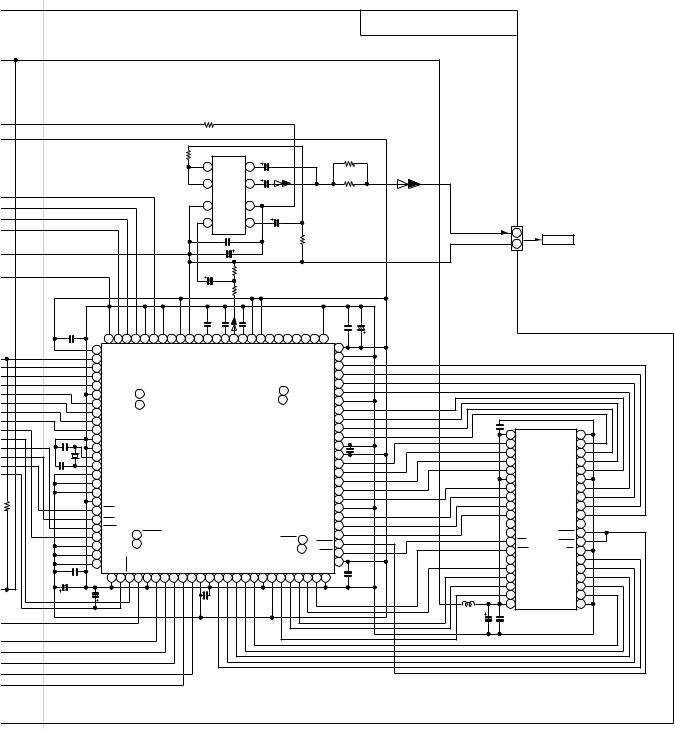
CD-K7000V,CP-C7000
CD VIDEO PWB-C(1/2)
 VIDEO SIGNAL
|
|
|
|
|
|
|
|
|
|
|
|
|
|
|
|
|
|
|
|
|
|
|
+B |
|
|
|
|
|
|
|
|
|
|
|
|
|
RV64 |
|
|
|
|
|
|
|
|
|
|
|
|
|
|
|
|
|
|
|
|
|
|
|
|
|
|
|
|
|
47 |
|
|
|
|
|
|
|
|
|
|
|
|
|
|
|
|
|
|
|
|
+B |
|
|
|
|
|
|
|
|
|
|
|
|
|
|
|
|
|
|
|
|
|
+B |
|
|
|
|
|
|
|
|
|
|
|
|
|
|
|
|
|
|
|
|
|
|
|
|
|
|
|
|
|
|
|
|
|
|
|
|
|
|
|
|
RV95 |
|
|
|
|
|
|
|
|
CV39 |
|
|
|
|
RV62 |
|
|
|
|
|
|
||
|
|
|
|
ICV4 |
6.8K |
|
|
4 |
|
|
|
5 |
1000/6.3 |
|
|
|
|
150 |
|
|
|
|
|
|
|
|||
|
|
|
|
|
|
|
|
|
|
|
|
|
|
|
|
|
RV63 |
|
|
|
|
|
|
|||||
|
|
|
NJM2267M |
|
|
|
|
|
|
|
|
|
|
|
|
|
|
|
|
|
|
|
|
|||||
|
|
|
|
VIDEO |
|
|
|
3 |
|
|
|
6 |
|
|
|
|
|
|
|
150 |
|
|
|
|
|
|
|
|
|
|
OPERATION AMP. |
|
|
|
|
|
|
|
|
CV40 |
|
|
|
|
|
|
|
|
|
|
|
|
|||||
|
|
|
|
|
|
|
|
|
2 |
|
|
|
7 |
22/6.3 |
|
|
|
|
|
|
|
|
|
|
|
|
||
|
|
|
|
|
|
|
|
|
|
|
|
|
|
CV41 |
|
|
|
|
|
|
|
|
|
|
|
|
||
|
|
|
|
|
|
|
|
|
1 |
|
|
|
8 |
|
|
4.7/25 |
|
|
|
|
|
|
|
|
|
|
|
|
|
|
|
|
|
|
|
|
|
|
|
|
|
|
|
|
|
|
|
|
|
|
|
1 |
|
P27 10 - A |
|||
|
|
|
|
|
|
|
|
|
CV17 |
|
0.01 |
|
|
RV96 |
|
|
|
|
|
|
|
|
||||||
|
|
|
|
|
|
|
|
|
|
|
|
|
|
|
|
|
|
|
|
CNS606 |
||||||||
|
|
|
|
|
|
|
|
|
|
|
|
33K |
|
|
|
|
|
|
|
2 |
|
|||||||
|
|
|
|
|
|
|
|
|
|
|
|
|
|
|
|
|
|
|
|
|
|
|
|
|||||
|
|
|
|
|
|
|
|
|
CV18 |
|
1000/6.3 |
|
|
|
|
|
|
|
TO MAIN PWB |
|||||||||
|
|
|
|
|
|
|
|
|
|
|
|
|
|
|
|
|
|
|
CNPV3 |
|||||||||
|
|
|
|
|
|
|
|
CV15 |
|
|
|
RV61 |
|
|
|
|
|
|
|
|
|
|
|
|
|
|||
|
|
|
|
|
|
|
|
4.7/25 |
|
|
|
100K |
|
|
|
|
|
|
|
|
|
|
|
|
|
|||
|
|
|
|
|
|
|
|
|
|
|
|
RV60 |
|
|
|
|
|
|
|
|
|
|
|
|
|
|
||
|
+B |
|
|
|
|
|
|
|
|
|
|
|
100 |
|
|
|
|
|
|
|
|
|
+B |
|
|
|
|
|
|
|
|
|
|
|
|
|
|
|
|
|
|
|
|
|
|
|
|
|
|
|
|
|
|
|
|
|
|
|
CV11 |
|
|
|
|
|
CV13 |
0.1 |
CV14 |
0.1 |
|
CV16 |
0.1 |
|
|
|
CV19 |
0.22 |
CV22 |
47/6.3 |
|
|
|
|
|
|||
|
0.22 |
|
|
|
|
|
|
|
|
|
|
|
|
|
|
|||||||||||||
|
|
100 9998 97 96 9594 93 9291 90 8988 8786 85 84 83 82 81 80 79 78 7776 |
|
|
|
|
|
|
|
|
|
|||||||||||||||||
|
+B |
1 VDD |
CDBCK |
CDLRCK |
CDEMPH CDC2PO GND |
VDD |
AGND |
VOUT3 |
CBP3 VOUT2 |
|
CBP2 |
VOUT1 |
CBP1 AVDD |
VDD |
HSYNC NSYNC |
CSYNC |
VDD 75 |
|
+B |
|
|
|
|
|
||||
|
|
|
|
|
|
|
|
|
||||||||||||||||||||
|
2 HD7 |
|
GND |
74 |
|
|
|
|
|
|
|
|||||||||||||||||
|
|
|
|
|
|
|
|
|
|
|||||||||||||||||||
|
|
3 HD6 |
|
MD8 |
73 |
|
|
|
|
|
|
|
||||||||||||||||
|
|
4 HD5 |
|
|
|
|
|
|
|
|
|
|
|
|
|
|
|
|
MD9 72 |
|
|
|
|
|
|
|
||
|
|
5 HD4 |
|
|
|
|
|
|
|
|
|
|
|
|
|
76 GND |
|
MD10 71 |
|
|
|
|
|
|
|
|||
|
|
6 GND |
|
99 |
CDI |
|
|
|
|
|
|
|
|
|
|
|
MD11 70 |
|
|
|
|
|
|
|
||||
|
|
|
|
|
|
|
|
|
|
|
|
|
77 VCLK |
|
|
|
|
|
|
|
||||||||
|
|
7 HD3 |
|
100 |
GND |
|
|
|
|
|
|
|
|
|
|
GND 69 |
|
|
|
|
|
|
|
|||||
|
|
8 HD2 |
|
|
|
|
|
|
|
|
|
|
|
|
|
|
|
|
MD12 68 |
|
|
|
|
|
|
|
||
|
CV6 |
9 HD1 |
|
|
|
|
|
|
|
|
|
|
|
|
|
|
|
|
MD13 67 |
|
|
CV24 |
|
|
|
|
||
XV2 |
10 HD0 |
|
|
|
|
|
|
|
|
|
|
|
|
|
|
|
|
MD14 66 |
|
|
0.22 |
1 VDD |
|
|
|
|||
27P(CH) |
|
|
|
|
ICV2 |
|
|
|
|
|
|
|
|
|
MD15 |
65 |
|
|
|
|
VSS 40 |
|||||||
11 GND |
|
|
|
|
|
|
|
|
|
|
|
|
|
|
|
|
|
|
||||||||||
27MHz |
|
|
|
|
|
|
|
|
|
|
|
|
|
|
|
|
|
2 DQ0 |
|
|
DQ15 39 |
|||||||
|
|
12 GND |
|
|
|
D61012GC |
|
|
|
|
|
|
|
GND 64 |
|
|
|
|
|
|||||||||
|
|
|
|
|
|
|
|
|
|
|
|
CV21 |
|
|
3 DQ1 |
|
|
DQ14 38 |
||||||||||
|
XV2 |
13 X1 |
|
|
|
|
|
|
|
|
|
|
VDD 63 |
|
|
|
|
|||||||||||
|
|
|
|
|
|
|
|
|
|
|
0.22 |
|
|
|
|
|||||||||||||
|
|
14 X2 |
|
|
MPEG DECODER |
|
|
|
|
|
MD0 62 |
|
|
|
4 DQ2 |
|
|
DQ13 37 |
||||||||||
|
CV7 |
15 VDD |
|
|
|
|
|
|
|
|
|
|
|
|
|
|
|
|
MD1 61 |
|
|
|
5 DQ3 |
|
|
DQ12 36 |
||
|
27P(CH) |
|
|
|
|
|
|
|
|
|
|
|
|
|
|
|
|
|
|
+B |
6 VDD |
|
|
VSS 35 |
||||
|
16 CKSEL |
|
|
|
|
|
|
|
|
|
|
|
|
|
|
|
|
MD2 60 |
|
|
|
|
||||||
RV50 3.9K |
|
17 VDD |
|
|
|
|
|
|
|
|
|
|
|
|
|
|
|
|
MD3 59 |
|
|
|
7 DQ4 |
|
|
DQ11 34 |
||
|
|
|
|
|
|
|
|
|
|
|
|
|
|
|
|
|
MD4 58 |
|
|
|
8 DQ5 |
|
SDM4260C DRAM |
DQ10 33 |
||||
|
18 GND |
|
|
|
|
|
|
|
|
|
|
|
|
|
|
|
|
|
|
|
|
|||||||
|
19 HCS |
|
|
|
|
|
|
|
|
|
|
|
|
|
|
|
|
GND 57 |
|
|
|
9 DQ6 |
ICV3 |
DQ9 32 |
||||
|
20 HRD |
|
|
|
|
|
|
|
|
|
|
|
|
|
|
|
|
MD5 56 |
|
|
|
10 DQ7 |
DQ8 31 |
|||||
|
|
|
|
|
|
|
|
|
|
|
|
|
|
|
|
|
MD6 55 |
|
|
|
11 |
30 |
||||||
|
21 HWR |
|
|
|
|
|
|
|
|
|
|
|
|
|
|
|
|
|
|
|
||||||||
|
22 HA |
|
27 RESET |
|
|
|
|
|
|
|
|
|
|
MRAS 49 |
MD7 54 |
|
|
|
12 |
LCAS 29 |
||||||||
|
23 HSELX |
|
26 GND |
|
|
|
|
|
|
|
|
|
|
MCAS 53 |
|
|
|
13 WE |
UCAS 28 |
|||||||||
|
|
AULRCK AUEMPH |
|
|
|
|
|
|
|
|
|
GND |
50 |
|
|
|
||||||||||||
+B |
24 HSELA |
HDAK |
|
GND AUCLK AUBCK |
AUDO |
|
|
|
|
|
|
|
|
|
MWE 52 |
|
|
|
14 RAS |
|
|
OE 27 |
||||||
|
|
|
VDD |
GND MA8 |
MA7 |
MA6 |
MA5 |
MA4 |
GND |
VDD MA3 MA2 |
MA1 |
MA0 |
VDD |
51 |
|
|
|
15 |
|
|
A8 26 |
|||||||
|
|
25 VDD |
INT |
|
+B |
|
|
|
||||||||||||||||||||
|
CV9 |
|
|
|
16 A0 |
|
|
A7 25 |
||||||||||||||||||||
|
0.22 |
26 2728 29 30 313233 34 35 36 37 383940 4142 43 44 45 4647 4849 50 |
|
CV20 |
|
|
17 A1 |
|
|
A6 24 |
||||||||||||||||||
|
|
|
0.22 |
|
|
|
|
|||||||||||||||||||||
|
CV10 |
CV3 |
|
|
|
|
CV12 0.22 |
|
|
|
|
|
|
|
|
|
|
|
|
|
|
L63 |
18 A2 |
|
|
A5 23 |
||
|
|
|
|
|
|
|
|
|
|
|
|
|
|
|
|
|
|
|
19 A3 |
|
|
A4 22 |
||||||
|
47/6.3 |
4.7/50 |
|
|
|
|
|
|
|
|
|
|
|
|
|
|
|
|
|
|
0.82 |
|
|
|
||||
|
|
|
|
|
|
|
|
|
|
|
|
|
|
|
|
|
|
|
|
H |
20 VDD |
|
|
VSS 21 |
||||
|
|
|
|
|
|
|
|
|
|
|
|
|
|
|
|
|
|
|
|
|
+B |
|
|
|
||||
|
+B |
|
|
|
|
|
|
|
|
|
|
|
|
|
|
|
|
|
|
|
|
|
|
|
|
|
|
|
|
|
|
|
|
|
|
|
|
|
|
|
|
|
+B |
|
|
|
|
|
|
|
CV23 |
CV25 |
|
|
|
||
|
|
|
|
|
|
|
|
|
|
|
|
|
|
|
|
|
|
|
|
|
|
|
47/6.3 |
0.22 |
|
|
|
|
7 |
8 |
9 |
10 |
11 |
12 |
Figure 23 SCHEMATIC DIAGRAM (3/13)
– 23 –

CD-K7000V,CP-C7000
A
CD VIDEO PWB-C(2/2)
|
|
|
|
|
|
|
|
|
|
|
|
|
|
|
|
|
|
|
|
CD SIGNAL |
|
||||||
|
|
|
|
CNS1B |
CNS1A |
|
|
|
|
|
|
|
|
+B |
|
|
|
|
|
|
|
|
|
|
|
|
|
B |
|
Vcc |
7 |
7 |
7 |
7 |
|
|
|
|
|
|
|
|
R50 |
|
|
|
|
|
|
|
|
|
|
|
|
|
Vref |
6 |
6 |
6 |
6 |
|
|
|
|
|
|
|
|
47 |
|
|
|
|
|
|
|
|
|
|
|
|
|
|
|
R51 |
68K |
|
|
|
|
|
TIN1 |
|
|
|
|
|
|
|
|
|
|
|
|
|
|||||
|
|
E |
5 |
5 |
5 |
5 |
|
|
|
|
|
|
|
|
|
|
|
|
|
|
|
|
|
|
|||
|
|
A |
R52 |
68K |
|
|
|
|
|
FIN1 |
|
|
|
|
|
|
|
|
|
|
|
|
|
||||
|
|
4 |
4 |
4 |
4 |
|
|
|
|
|
|
|
|
IC1 |
|
|
|
|
|
|
|
||||||
|
|
B |
R53 |
68K |
|
|
|
|
|
FIN2 |
|
|
|
|
|
|
|
|
|
|
|||||||
|
|
3 |
3 |
3 |
3 |
|
|
|
|
|
|
|
|
|
|
|
|
|
|
|
|||||||
|
|
|
|
|
|
|
|
|
|
|
|
|
|
|
|
|
|
|
|
|
|
|
|
||||
|
|
F |
2 |
2 |
2 |
2 |
R54 |
68K |
|
|
|
|
|
TIN2 |
|
|
LA9235M |
|
|
|
|
|
|
|
|||
|
|
|
|
|
|
|
R56 |
|
R55 |
|
|
|
|
|
|
|
C11 |
||||||||||
|
|
|
|
|
|
|
|
|
|
|
|
|
|
SERVO AMP. |
|
|
|
|
|
||||||||
|
|
C |
1 |
1 |
1 |
1 |
|
|
|
|
68K |
|
68K |
|
|
|
|
|
|
47/6.3 |
|||||||
|
|
|
|
|
|
|
|
|
|
|
|
|
|
|
|
|
|
|
|
|
|
|
|||||
|
|
|
|
|
|
|
|
|
|
|
FIN1 1 |
|
|
|
|
|
30 VCC |
|
|
C12 |
|||||||
|
|
|
|
|
|
|
CNP1 |
|
|
|
|
|
|
|
|
|
|
|
|
|
|
||||||
|
|
|
|
|
|
|
|
|
|
|
|
|
|
|
|
|
REF |
|
|
ODRV RFSW |
|
|
0.022 |
||||
|
|
|
|
|
|
|
|
|
|
|
|
|
|
|
FIN2 2 |
|
|
|
|
6.8K |
|
||||||
|
|
|
|
|
|
|
|
|
|
|
|
|
|
|
|
|
|
REF |
|
29 |
R42 |
R7 |
|
||||
|
|
|
|
|
|
|
|
|
|
|
|
C54 |
47/10 |
C55 0.01 |
|
|
REF |
|
|
AGCON |
|
|
120K |
C18 |
|||
C |
|
|
|
|
|
|
|
|
|
|
|
|
|
|
|
|
|
|
|
39K |
R6 27K |
||||||
|
|
|
|
|
|
|
|
|
|
|
|
|
REF |
|
|
|
|
|
|
||||||||
|
|
|
|
|
|
|
|
|
|
|
|
|
|
|
TIN1 3 |
|
|
|
|
|
28 RF– |
|
R5 |
(CH) |
|||
|
|
|
|
|
|
|
|
|
|
|
|
|
|
|
|
|
|
|
|
|
|
|
|
|
|
||
|
|
|
|
|
|
|
|
|
|
|
|
|
|
|
TIN2 |
4 |
|
|
|
PH REF |
27 RF |
|
|
|
|
||
|
|
|
|
|
|
|
|
|
|
|
|
|
|
|
C6 |
|
|
|
|
|
|
|
|
|
C13 |
|
|
|
|
|
|
|
|
|
|
|
|
|
|
|
|
|
100/6.3 |
REF |
|
|
|
|
26 |
|
|
|
|||
|
|
|
|
|
|
|
|
|
|
|
|
|
|
C8 |
|
|
|
|
|
|
0.01 |
|
|||||
|
|
|
|
|
|
|
|
|
|
|
|
|
|
REF1 |
5 |
|
|
|
|
|
25 PH |
|
|
||||
|
|
|
|
|
|
|
|
|
|
|
|
|
|
REF |
|
|
DH |
|
|
|
|
|
|||||
|
|
|
|
|
|
|
|
|
|
|
|
|
|
0.022 |
VREF 6 |
|
|
|
24 BH |
|
C14 |
|
|||||
|
|
|
|
|
|
|
|
|
|
|
|
|
|
|
|
|
|
|
|
|
|
||||||
|
|
|
|
|
|
|
|
|
|
|
|
|
|
C7 |
|
7 |
|
|
ODRV |
|
23 |
|
|
0.33 |
|
||
|
|
|
|
|
|
|
|
|
|
|
|
|
|
10/16 |
|
APC |
|
|
|
|
|
|
|
|
|
||
|
|
|
|
|
|
|
|
|
|
|
|
|
|
LDD 8 |
|
PH/BH |
|
22 RFEV |
|
|
|
||||||
|
|
|
|
|
|
|
|
|
|
|
|
|
|
|
|
|
|
|
|
||||||||
|
|
|
|
|
|
|
|
|
|
|
|
|
|
|
GND 9 |
|
|
|
REF |
|
21 FE– |
|
|
|
|
||
|
|
|
|
|
|
|
|
|
|
|
|
|
|
|
LDON |
|
|
|
|
LPF |
|
20 FE |
R3 |
|
|
||
|
|
|
|
|
|
|
|
|
|
|
|
|
|
|
10 |
|
REF REF |
|
|
|
|||||||
|
|
|
|
|
|
|
|
|
|
C53 |
C51 |
|
|
R25 |
|
11 |
ODRV |
|
|
LPF |
|
19 TE–82K |
|
|
|||
|
|
|
|
|
|
|
|
|
|
0.001 |
47/6.3 +B |
10K |
AGON 12 |
AGCON |
|
|
REF |
|
18 TE |
R4 |
|
|
|||||
|
|
|
|
|
|
|
|
|
|
|
|
|
|
|
REF |
|
|
|
|
||||||||
|
|
|
|
|
|
|
|
|
|
|
|
|
|
|
EFBL |
13 |
|
REF |
|
17 |
HFL18K |
|
|
||||
|
|
|
|
|
|
|
|
|
|
|
R47 |
|
|
TEST0 |
|
|
|
|
|
|
|
|
|||||
|
|
|
|
|
|
|
|
|
|
|
|
|
|
LPF |
|
REF |
|
16 |
TEST |
|
|
||||||
|
|
|
|
|
|
|
|
|
|
|
|
|
14 |
|
|
|
|
||||||||||
D |
|
|
|
|
|
|
|
|
|
|
3.3 |
|
|
|
TES115 |
REF |
|
|
|
|
|
|
|
|
|
||
|
|
|
|
|
|
|
|
|
|
|
|
|
|
|
|
|
|
4 |
|
|
|
|
|||||
|
|
|
|
|
|
|
|
|
|
Q3 |
|
|
|
|
|
|
|
|
|
|
|
|
|
|
|
||
|
|
|
|
|
|
|
|
|
|
|
|
|
|
|
|
|
|
|
|
|
|
|
|
|
|
||
|
|
|
|
|
|
|
|
|
|
KTA1504 GR |
|
|
|
|
|
|
|
|
|
|
|
|
|
|
|
||
|
|
|
|
|
|
|
|
|
|
LASER |
|
|
|
|
|
|
|
|
|
|
|
|
|
|
|
||
|
|
|
|
|
|
|
|
|
|
DRIVER |
|
|
|
|
|
|
|
|
|
|
|
|
|
|
|
|
|
|
|
|
|
|
|
|
|
|
|
|
|
|
|
|
|
|
|
|
|
13 |
|
|
|
|
|
|
|
|
|
|
|
|
|
|
|
|
|
|
C52 |
|
|
|
|
|
|
|
|
|
|
|
|
|
|
|
|
E |
|
|
|
|
|
|
|
|
|
|
0.01 |
+B |
|
|
|
|
|
|
|
|
|
|
|
|
|
|
|
|
|
|
|
|
|
|
|
|
|
|
|
|
|
|
|
|
|
|
|
|
|
|
|
|
|
|
|
|
|
|
|
|
|
|
|
|
|
|
|
|
|
|
|
|
TDO |
TO 1 |
– |
|
|
|
|
|
+ |
|
|
|
|
TR- |
1 |
1 |
1 |
1 |
TR– |
|
|
|
|
|
|
|
|
|
FDO |
FD |
2 |
+ |
+– |
|
|
|
|
– |
+ |
|
TR+ |
|
TR+ |
|
|
|
|
|
|
|
|
|
|
FO |
– |
|
|
|
|
|
|
– |
|||||
|
TR+ |
2 |
2 |
2 |
2 |
|
|
|
|
|
|
|
|
|
C46 |
3 |
|
|
|
|
|
|
+ |
||||
|
|
|
|
|
|
|
|
|
|
|
|
|
|
+ |
– |
|
|
|
|
|
|||||||
|
FO+ |
|
|
|
|
3 |
FO+ |
|
|
|
|
|
|
|
|
|
0.022 |
FO+ 4 |
|
|
|
|
|
|
– |
||
|
FO+ |
3 |
3 |
3 |
|
|
|
|
|
|
|
|
|
|
+ |
|
|
|
|
|
|
||||||
|
|
FO- |
4 |
4 |
4 |
4 |
FO– |
|
|
|
|
|
|
|
|
|
|
FO– 5 |
|
|
|
|
|
|
|
|
|
|
FO- |
GND |
5 |
5 |
5 |
5 |
GND |
|
|
|
|
|
|
|
|
|
|
TR+ 6 |
|
|
|
|
|
|
|
|
|
|
|
6 |
6 |
6 |
6 |
PD |
|
|
|
|
|
|
|
|
|
|
TR– 7 |
|
|
|
|
|
|
|
|
||
|
TR- |
PD |
|
|
|
|
|
|
|
|
|
|
|
M63001FP |
|
|
|
|
|
||||||||
|
|
CNS2B |
CNS2A |
7 |
VR |
|
|
|
|
|
|
|
|
|
|
|
8 |
IC3 |
|
|
|
|
|
||||
|
|
VR |
7 |
7 |
7 |
LD |
|
|
|
|
|
|
|
|
|
|
|
|
|
|
|
|
|
|
|
||
|
|
|
|
|
|
|
|
|
|
|
|
|
9 |
|
|
|
|
|
|
|
|
||||||
|
ACTUATOR |
LD |
8 |
8 |
8 |
8 |
|
|
|
|
IC3 |
|
|
|
|
|
|
|
|
|
|
|
|
|
|
|
|
|
|
|
|
|
|
|
CNP2 |
|
|
|
|
|
|
|
|
|
|
10 |
|
|
|
|
|
|
|
|
|
F |
PICKUP UNIT |
|
|
|
|
|
|
|
FOCUS/TRACKING/ |
|
|
|
GND 11 |
|
|
|
|
|
|
|
|
||||||
|
|
|
|
|
|
|
|
|
|
|
12 |
|
|
|
|
|
|
|
|
||||||||
|
|
|
|
|
|
|
|
SPIN/SLED DRIVER |
|
|
|
|
|
|
|
|
|
|
|
|
|||||||
|
|
|
|
|
|
|
|
|
|
|
|
|
|
13 |
|
|
|
|
|
|
|
|
|||||
|
|
|
|
|
|
|
|
|
|
|
|
|
|
|
|
|
|
|
14 |
|
|
|
|
|
|
|
|
|
|
|
|
|
|
|
|
|
|
|
|
|
|
|
|
|
|
SL– 15 |
|
|
|
|
|
|
|
|
|
|
|
|
|
|
|
|
|
|
|
|
|
|
|
|
|
|
|
SL+ 16 |
– |
|
|
|
|
|
|
|
|
|
|
|
|
|
|
|
|
|
|
|
|
|
|
|
|
|
SLDO |
17 |
– |
|
|
|
|
|
|
||
|
|
|
|
|
|
|
|
|
|
|
|
|
|
|
|
|
|
|
+ |
|
|
|
|
|
|
||
|
|
|
|
|
|
|
|
|
|
|
|
|
|
|
|
|
+B |
VCC1 18 |
|
+ |
|
|
|
|
|
|
|
|
|
|
|
|
|
|
|
|
|
|
|
|
|
|
|
|
+ |
|
|
|
|
|
– |
– |
|||
|
|
|
|
|
|
|
|
|
|
|
|
|
|
|
|
|
STANDBY |
|
– |
|
|
|
|
|
+ |
||
|
|
|
|
|
|
|
|
|
|
|
|
|
|
|
R48 |
19 |
|
|
|
|
|
|
+ |
+ |
|||
|
CD MOTOR PWB-F |
|
|
|
|
|
|
|
|
|
|
6.8K |
|
Vref 20 |
|
|
|
|
|
|
+ |
– |
|||||
|
|
|
|
|
|
|
|
|
|
|
C50 |
|
|
|
|
|
|
|
|
+ |
|||||||
|
|
|
CNS3B |
CNS3A |
|
CNP3 |
|
|
|
|
|
MUTE |
|
|
|
|
|
|
|
– |
|||||||
|
M1 |
|
|
CNP3A |
|
|
|
|
|
|
+B |
|
|
21 |
|
|
|
|
|
|
|
– |
|||||
|
|
|
|
|
|
|
|
|
|
|
|
|
|
|
100/6.3 |
|
|
|
|
|
|
|
|
|
|||
G |
SPINDLE |
+ |
|
|
6 |
|
6 |
6 |
6 |
SP– |
|
|
|
|
|
|
C49 |
|
|
|
|
|
|
|
|
|
|
MOTOR |
M - |
|
|
|
SP+ |
|
|
|
|
|
|
100/6.3 |
|
|
|
|
|
|
|
|
|
||||||
|
|
5 |
|
5 |
5 |
5 |
|
|
|
|
|
|
|
|
|
|
|
|
|
|
|
||||||
|
M2 |
+ |
|
|
|
SL+ |
|
|
|
|
|
|
|
|
|
|
|
|
|
|
|
|
|
||||
|
|
|
4 |
|
4 |
4 |
4 |
|
|
|
|
|
|
|
|
|
|
|
|
|
|
|
|
|
|||
|
M - |
|
|
|
SL– |
|
|
|
|
|
|
|
|
|
|
|
|
|
|
|
|
|
|||||
|
SLED |
|
|
|
|
|
|
|
|
|
|
|
|
|
|
|
|
|
|
|
|
||||||
|
|
|
3 |
|
3 |
3 |
3 |
|
|
|
|
|
|
|
|
|
|
|
|
|
|
|
|
|
|||
|
MOTOR |
|
|
|
PUIN |
|
|
|
|
|
|
|
|
|
|
|
|
|
|
|
|
|
|||||
|
|
|
|
2 |
|
2 |
2 |
2 |
|
|
|
|
|
|
|
|
|
|
|
|
|
|
|
|
|
||
|
|
|
|
|
|
GND(D) |
|
|
|
|
|
|
|
|
|
|
|
|
|
|
|
|
|
||||
|
SW4 |
|
|
|
1 |
|
1 |
1 |
1 |
|
|
|
|
|
|
|
|
|
|
|
|
|
|
|
|
|
|
|
|
|
|
|
|
|
|
|
|
|
|
|
|
|
|
|
|
|
|
|
|
|
|||||
|
PICKUP IN |
|
|
|
|
|
|
|
|
|
|
|
|
|
|
|
|
|
|
|
|
|
|
|
|
|
|
H
• NOTES ON SCHEMATIC DIAGRAM can be found on page 16.
|
|
|
|
|
|
|
IC |
|
|
|
|
|
|
SERV |
|||
|
|
|
|
|
|
CONT |
||
|
|
8 |
|
|
7 |
|
||
|
|
C23 |
R12 |
|
|
|
|
|
5 |
0.047 |
680 |
|
|
|
PDO1 |
1 |
|
R79 |
|
|
R13 |
|
||||
|
|
|
|
|||||
1.5M |
C24 |
680 |
|
PDO2 |
2 |
|||
|
|
2.2/50 |
|
|
|
VVSS |
||
|
|
|
|
|
3 |
|||
|
|
C21 |
|
|
|
|||
C25 |
0.022 |
R11 |
C81 |
|
||||
C22 |
PCKIST 4 |
|||||||
|
|
0.1 |
|
0.022 |
|
|||
|
|
100P |
12K |
|
|
VVDD 5 |
||
R10 |
R80 |
R14 |
|
|
FR 6 |
|||
27K |
1M |
1.2K |
|
|
HFL 7 |
|||
C20 |
|
|
|
|
|
|||
|
R15 |
|
|
|
SLCIST 8 |
|||
0.1 |
|
|
|
|
||||
R8 |
10K |
|
|
|
SLCO |
9 |
||
|
330 |
|
|
|
|
EFMIN |
||
|
|
|
|
|
10 |
|||
C17 |
|
|
|
C27 |
|
JITTV |
||
0.0047 C42 |
|
|
0.1 |
|
|
11 |
||
C26 |
|
JITTC 12 |
||||||
|
68P |
|
|
|
||||
|
(CH) |
0.047 |
|
|
|
BH |
13 |
|
|
|
|
|
|
|
|
|
|
|
|
|
|
PH(RFENV) 14 |
||||
|
|
|
|
|
|
|
FE 15 |
|
|
|
|
|
|
|
|
TE 16 |
|
|
|
|
C28 |
|
|
VREF 17 |
||
C82 |
|
|
47/10 |
ADAVDD 18 |
||||
|
|
|
|
|
|
|
|
|
0.022 |
|
|
|
ADAVSS 19 |
||||
|
C41 |
|
C29 |
|||||
|
|
|
PHREF |
20 |
||||
|
100/6.3 |
|
0.022 |
|
|
|||
|
|
|
|
|
|
BHREF 21 |
||
|
|
|
|
R44 TBLO |
22 |
|||
|
|
|
|
1K |
|
|
23 |
|
|
|
1 |
EFBL TDO |
FDO |
|
|||
|
|
|
24 |
|||||
R37 |
|
|
R35 |
1K |
|
2 |
||
15K |
|
|
|
|||||
|
|
|
|
|
||||
|
|
|
|
TDO |
FDO |
6 |
||
|
|
|
|
|
|
|
||
+B
42 |
LD_M+ |
|
41 |
LD_M– |
|
40 |
VCC4 |
+B |
39 |
LOADING M+ |
|
38 |
LOADING M– |
|
37 |
|
C47 |
36 |
|
|
|
100/6.3 |
|
35 |
|
|
|
|
|
34 |
|
|
33 |
GND |
|
32 |
|
|
31 |
|
|
30 |
|
|
29 |
VCC3 |
+B |
28 |
SP– |
|
27 |
SP+ |
|
26 |
SPO SPDO |
|
25 |
|
|
24 VCC2(SPN) |
||
23 |
|
|
22 |
|
|
|
|
+B |
|
1 |
2 |
3 |
4 |
5 |
6 |
Figure 24 SCHEMATIC DIAGRAM (4/13)
– 24 –
 Loading...