


CD-DP2500W/DK2500W
SERVICE MANUAL
No. S4034CDDP2500
CD-DP2500W
CD-DP2500W Mini Component System consisting of CDDP2500W (main unit), CP-DP2500 (front speakers), GBOXS0038AWM1 (centre speaker) and GBOXS0039AWM1 (surround speakers).
CD-DP2500W |
CD-DK2500W |
CD-DK2500W
CD-DK2500W Mini Component System consisting of CDDK2500W (main unit), CP-DP2500 (front speakers), GBOXS0038AWM1 (centre speaker) and GBOXS0039AWM1 (surround speakers).
DIFFERENCE BETWEEN CD-DP2500W AND CD-DK2500W
SECTION |
CD-DP2500W |
CD-DK2500W |
KARAOKE |
Non |
Used |
|
|
|
Manufactured under license from Dolby Laboratories Licensing Corporation.
DOLBY, the double-D symbol  and "PRO LOGIC" are trademarks of Dolby Laboratories Licensing Corporation.
•In the interests of user-safety the set should be restored to its original condition and only parts identical to those specified be used.
CONTENTS |
|
|
Page |
SAFETY PRECAUTION FOR SERVICE MANUAL ........................................................................................................... |
2 |
VOLTAGE SELECTION ..................................................................................................................................................... |
2 |
SPECIFICATIONS ............................................................................................................................................................. |
3 |
NAMES OF PARTS ........................................................................................................................................................... |
4 |
OPERATION MANUAL ...................................................................................................................................................... |
8 |
DISASSEMBLY .................................................................................................................................................................. |
9 |
REMOVING AND REINSTALLING THE MAIN PARTS ................................................................................................... |
12 |
TEST MODE .................................................................................................................................................................... |
13 |
ADJUSTMENT ................................................................................................................................................................. |
14 |
NOTES ON SCHEMATIC DIAGRAM .............................................................................................................................. |
16 |
BLOCK DIAGRAM ........................................................................................................................................................... |
17 |
SCHEMATIC DIAGRAM / WIRING SIDE OF P.W.BOARD .............................................................................................. |
20 |
VOLTAGE ........................................................................................................................................................................ |
42 |
WAVEFORMS OF CD CIRCUIT ...................................................................................................................................... |
43 |
TROUBLESHOOTING (CD SECTION) ........................................................................................................................... |
44 |
FUNCTION TABLE OF IC ................................................................................................................................................ |
48 |
FL DISPLAY ...................................................................................................................................................................... |
54 |
REPLACEMENT PARTS LIST/EXPLODED VIEW |
|
This document has been published to be used
SHARP CORPORATION for after sales service only.
The contents are subject to change without notice.
CD-DP2500W/DK2500W
SAFETY PRECAUTION FOR
SERVICE MANUAL
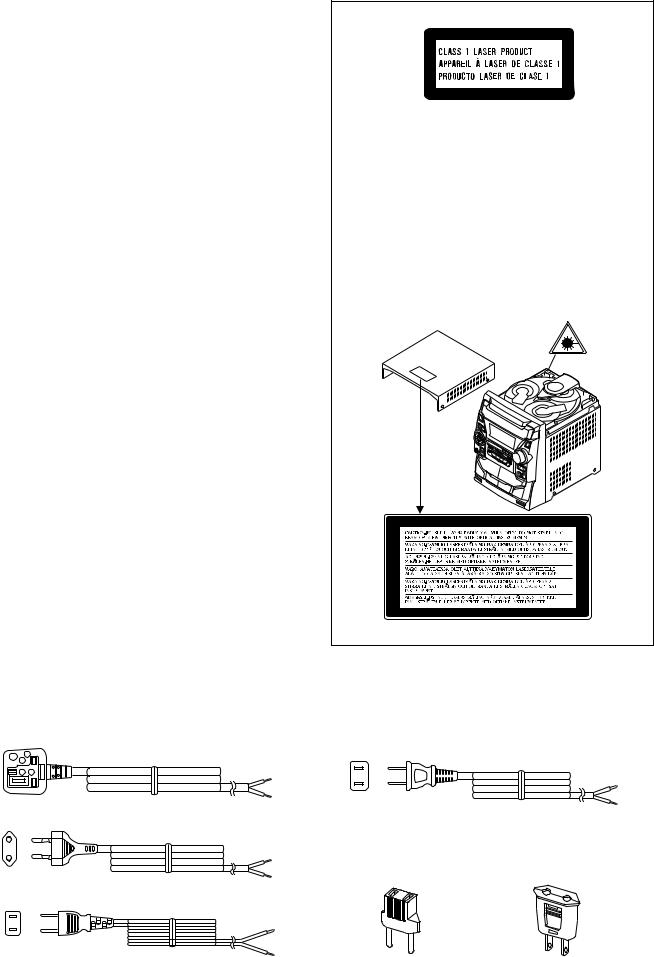
Precaution to be taken when replacing and servicing the Laser Pickup.
The AEL (Accessible Emission Level) of Laser Power Output for this model is specified to be lower than Class I Requirements. However, the following precautions must be observed during servicing to protect your eyes against exposure to the Laser beam
(1)When the cabinet has been removed, the power is turned on without a compact disc, and the Pickup is on a position outer than the lead-in position, the Laser will light for several seconds to detect a disc. Do not look into the Pickup Lens.
(2)The Laser Power Output of the Pickup inside the unit and replacement service parts have already been adjusted prior to shipping.
(3)No adjustment to the Laser Power should be attempted when replacing or servicing the Pickup.
(4)Under no circumstances look directly into the Pickup Lens at any time.
(5)CAUTION - Use of controls or adjustments, or performance of procedures other than those specified herein may result in hazardous radiation exposure.
CAUTION
●This Mini Component System is classified as a CLASS 1
LASER product.
●The CLASS 1 LASER PRODUCT label is located on the rear cover.
●Use of controls, adjustments or performance of procedures other than those specified herein may result in hazardous radiation exposure.
As the laser beam used in this compact disc player is harmful to the eyes, do not attempt to disassemble the cabinet. Refer servicing to qualified personnel only.
Laser Diode Properties
Material: GaAIAs
Wavelength: 780 nm
Emission Duration: continuous
Laser Output: max. 0.6 mW
Illustration:CD-DP2500W
VOLTAGE SELECTION
The voltage selector is located on the AC voltage selector box. If adjustment is necessary, ensure to remove plug of AC cord from AC socket and use a screwdriver in order to turn the selector in either direction. The correct voltage figure is displayed in the window below to the adjustment screw.
QACCB0006AW00 |
QACCA0003AW00 |
QACCE0010AW00
QPLGA0003AWZZ QPLGA0004AWZZ
QACCJ0007AW00
Figure 2 POWER SUPPLY CORD
– 2 –

CD-DP2500W/DK2500W
FOR A COMPLETE DESCRIPTION OF THE OPERATION OF THIS UNIT, PLEASE REFER TO THE OPERATION MANUAL.
SPECIFICATIONS
● General
Power source: |
AC 110/127/220/230-240 V, 50/60 Hz |
Power consumption: |
155 W |
Dimensions: |
Width; 270 mm (10-5/8") |
|
Height; 330 mm (13") |
|
Depth; 332 mm (13-1/16") |
Weight: |
8.9 kg (19.6 lbs.) |
● Amplifier section
Output power: |
Front speakers; |
|
MPO; 200 W (100W + 100 W) |
|
(10 % T.H.D.) |
|
RMS; 120 W (60 W + 60 W) |
|
(10 % T.H.D.) |
|
RMS; 96 W (48 W + 48 W) |
|
(0.9 % T.H.D.) |
|
Centre speaker; |
|
MPO; 50 W (10 % T.H.D.) |
|
RMS; 30 W (10 % T.H.D.) |
|
RMS; 24 W (0.9 % T.H.D.) |
|
Surround speakers; |
|
MPO; 50 W (25 W + 25 W) |
|
(10 % T.H.D.) |
|
RMS; 30 W (15 W + 15 W) |
|
(10 % T.H.D.) |
|
RMS; 24 W (12 W + 12 W) |
|
(0.9 % T.H.D.) |
Output terminals: |
Front speakers; 6 ohms |
|
Centre speaker; 6 ohms |
|
Surround speakers; 12 ohms |
|
Headphones; 16-50 ohms |
|
(recommended; 32 ohms) |
|
CD digital output (optical) |
Input terminals: |
Video/Auxiliary (audio signal) × 2; |
(CD-DP2500W) |
500 mV/47 kohms |
Input terminals: |
Video/Auxiliary (audio signal) × 2; |
(CD-DK2500W) |
500 mV/47 kohms |
|
Microphone 1/2; 1 mv/600 kohms |
● Compact disc player section
Type: |
3-disc multi-play compact disc player |
Signal readout: |
Non-contact, 3-beam semiconductor |
|
laser pickup |
D/A converter: |
1-bit D/A converter |
Frequency response: |
20 - 20,000 Hz |
Dynamic range: |
90 dB (1 kHz) |
● Tuner section
Frequency range: |
FM; 88-108 MHz |
|
AM; 531-1,602 kHz |
● Cassette deck section
Frequency response: |
50-14,000 Hz (Normal tape) |
Signal/noise ratio: |
55 dB (TAPE 1, playback) |
|
50 dB (TAPE 2, recording/playback) |
Wow and flutter: |
0.3 % (WRMS) |
● Front speaker section
Type: |
3-way type [13 cm (5-1/4") woofer, |
|
5 cm (2") tweeter and super tweeter] |
Maximum input |
|
power: |
120 W |
Rated input power: |
60 W |
Impedance: |
6 ohms |
Dimensions: |
Width; 240 mm (9-1/2") |
|
Height; 330 mm (13") |
|
Depth; 255 mm (10-1/16") |
Weight: |
3.9 kg (8.5 lbs.)/each |
● Centre speaker section
Type: |
10 cm (4") full-range speaker |
Maximum input |
|
power: |
60 W |
Rated input power: |
30 W |
Impedance: |
6 ohms |
Dimensions: |
Width; 260 mm (10-1/4") |
|
Height; 140 mm (5-1/2") |
|
Depth; 155 mm (6-1/8") |
Weight: |
0.9 kg (2.0 lbs.) |
● Surround speaker section
Type: |
10 cm (4") full-range speaker |
Maximum input |
|
power: |
30 W |
Rated input power: |
15 W |
Impedance: |
12 ohms |
Dimensions: |
Width; 200 mm (7-7/8") |
|
Height; 93 mm (3-11/16") |
|
Depth; 170 mm (6-3/4") |
Weight: |
0.5 kg (1.1 lbs.)/each |
Specifications for this model are subject to change without prior notice.
– 3 –
CD-DP2500W/DK2500W
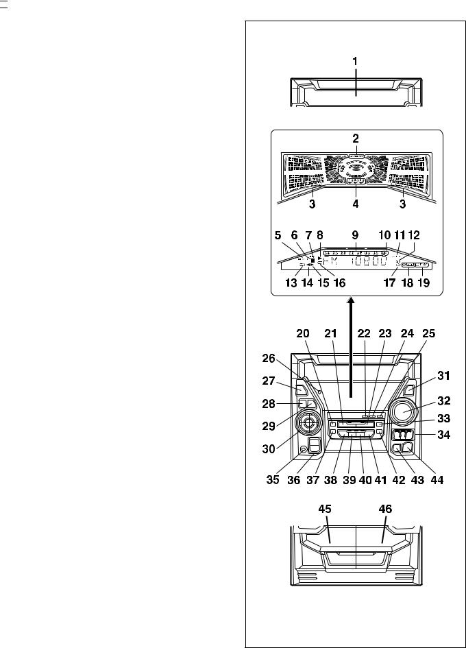
NAMES OF PARTS

 Front panel [CD-DP2500W]
1.(CD) Disc Tray
2.Extra Bass Indicator
3.Spectrum Analyzer/Volume Level Indicator
4.(CD) Disc Number Indicators
5.(CD/TUNER) Memory Indicator
6.(CD) Pause Indicator
7. (TAPE 2) Record Indicator
8. (CD) Play Indicator
9. (CD) Music Schedule Indicators
0. (CD) More Tracks Indicator
11.Sleep Indicator
12.FM Stereo Mode Indicator
13.(TAPE) Reverse Mode Indicator
14. (TAPE 2) Reverse Play Indicator
15. (TAPE 1) Play Indicator
(TAPE 2) Forward Play Indicator
16. (CD) Repeat Indicator
17. FM Stereo Indicator
18.Timer Record Indicator
19.Timer Play Indicator
20. Memory/Set Button
21. (CD) Track Down/Review Button
(TUNER) Preset Down Button
(TAPE 2) Fast Wind Button
22.Bypass Button
23.(CD) Track Up/Cue Button (TUNER) Preset Up Button (TAPE 2) Fast Wind Button
24.Normal Button
25.Phantom Button
26.Timer Set Indicator
27.On/Stand-by Button
28. Clock Button
29. Timer/Sleep Button
30. Function Selector Buttons
31.Dimmer Button
32.Volume Control
33.Equalizer Mode Selector Button
34. (CD) Disc Number Select Buttons
35. Headphone Socket
36. Tuning and Time Up/Down Buttons
37. (TAPE 2) Record Pause Button
38.(TAPE 2) Reverse Play Button
39.(CD/TAPE) Stop Button
40.(TAPE 2) Reverse Mode Button
41.(CD) Play/Repeat Button (TAPE 1) Play Button
(TAPE 2) Forward Play Button
42. Extra Bass/Demo Mode Button
43. (CD) Disc Skip Button
44.(CD) Open/Close Button
45.(TAPE 1) Cassette Compartment
46.(TAPE 2) Cassette Compartment
– 4 –
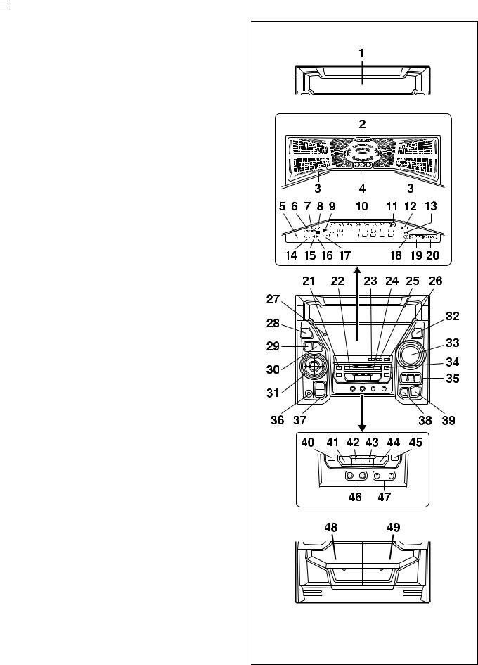

 Front panel [CD-DK2500W]
1.(CD) Disc Tray
2.Extra Bass Indicator
3.Spectrum Analyzer/Volume Level Indicator
4.(CD) Disc Number Indicators
5.Karaoke Maker Indicator
6.(CD/TUNER) Memory Indicator
7.(CD) Pause Indicator
8.(TAPE 2) Record Indicator
9.(CD) Play Indicator
(CD) Music Schedule Indicators
(CD) More Tracks Indicator
12.Sleep Indicator
13.FM Stereo Mode Indicator
14.(TAPE) Reverse Mode Indicator
15.(TAPE 2) Reverse Play Indicator
16.(TAPE 1) Play Indicator
(TAPE 2) Forward Play Indicator
17.(CD) Repeat Indicator
18.FM Stereo Indicator
19.Timer Record Indicator
20.Timer Play Indicator
21.Memory/Set Button
22.(CD) Track Down/Review Button (TUNER) Preset Down Button (TAPE 2) Fast Wind Button
23.Bypass Button
24.(CD) Track Up/Cue Button (TUNER) Preset Up Button (TAPE 2) Fast Wind Button
25.Normal Button
26.Phantom Button
27.Timer Set Indicator
28.On/Stand-by Button
29.Clock Button
30.Timer/Sleep Button
31.Function Selector Buttons
32.Dimmer Button
33.Volume Control
34.Equalizer Mode Selector Button
35.(CD) Disc Number Select Buttons
36.Headphone Socket
37.Tuning and Time Up/Down Buttons
38.(CD) Disc Skip Button
39.(CD) Open/Close Button
40.(TAPE 2) Record Pause Button
41.(TAPE 2) Reverse Play Button
42.(CD/TAPE) Stop Button
43.(TAPE 2) Reverse Mode Button
44.(CD) Play/Repeat Button (TAPE 1) Play Button
(TAPE 2) Forward Play Button
45.Extra Bass/Demo Mode Button
46.Microphone Sockets
47.Microphone Level Controls
48.(TAPE 1) Cassette Compartment
49.(TAPE 2) Cassette Compartment
CD-DP2500W/DK2500W |
– 5 –
CD-DP2500W/DK2500W

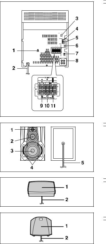
 Rear panel
1. AC Voltage Selector
2. AC Power Lead
3. CD Digital Output Socket
4. FM 75 Ohms Aerial Terminal
5. FM Aerial Earth Terminal
6. AM Loop Aerial Input Socket
7. Span Selector Switch
8. Video/Auxiliary (Audio Signal) Input Sockets
9. Front Speaker Terminals
10. Centre Speaker Terminals
11. Surround Speaker Terminals

 Front speaker
1. Super Tweeter
2. Tweeter
3. Woofer
4. Bass Reflex Ducts
5. Speaker Wire

 Centre speaker
1. Full-Range Speaker
2. Speaker Wire

 Surround speaker
1. Full-Range Speaker
2. Speaker Wire
– 6 –
CD-DP2500W/DK2500W

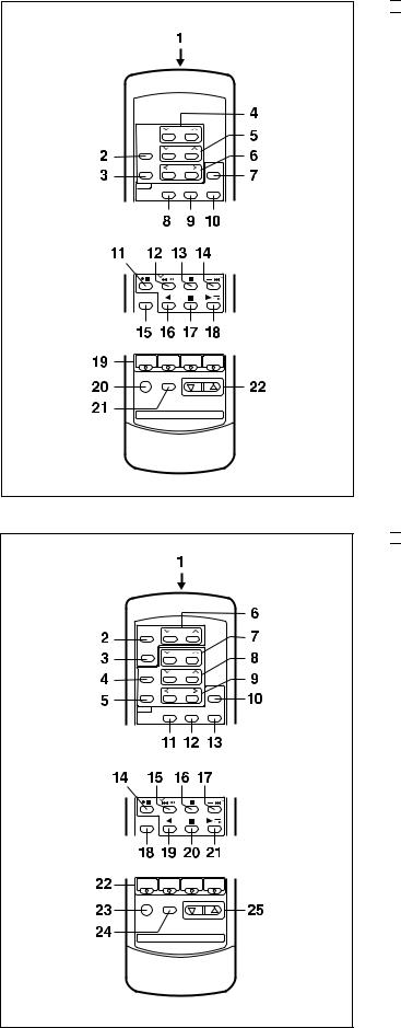
 Remote control [CD-DP2500W]
1.Remote Control Transmitter LED
2.Dolby Pro Logic Surround Mode Button
3.Test Tone Button
4.Centre Level Buttons
5.Surround Level Buttons
6.Balance Control Buttons
7.(CD) Disc Skip Button
8.(CD) Clear Button
9.(CD) Memory Button
10.(CD) Random Button
11.(TAPE 2) Record Pause Button
12.(CD) Track Down/Review Button (TUNER) Preset Down Button (TAPE 2) Fast Wind Button
13.(CD) Pause Button
14.(CD) Track Up/Cue Button (TUNER) Preset Up Button (TAPE 2) Fast Wind Button
15.Equalizer Mode Selector Button
16.(TAPE 2) Reverse Play Button
17.(CD/TAPE) Stop Button
18.(CD) Play/Repeat Button (TAPE 1) Play Button
(TAPE 2) Forward Play Button
19.Function Selector Buttons
20.On/Stand-by Button
21.Extra Bass Button
22.Volume Up/Down Buttons

 Remote control [CD-DK2500W]
1.Remote Control Transmitter LED
2.Karaoke Mode Button
3.Vocal Replacer Button
4.Dolby Pro Logic Surround Mode Button
5.Test Tone Button
6.Echo Level Up/Down Buttons
7.Centre Level Buttons
8.Surround Level Buttons
9.Balance Control Buttons
10.(CD) Disc Skip Button
11.(CD) Clear Button
12.(CD) Memory Button
13.(CD) Random Button
14.(TAPE 2) Record Pause Button
15.(CD) Track Down/Review Button (TUNER) Preset Down Button (TAPE 2) Fast Wind Button
16.(CD) Pause Button
17.(CD) Track Up/Cue Button (TUNER) Preset Up Button (TAPE 2) Fast Wind Button
18.Equalizer Mode Selector Button
19.(TAPE 2) Reverse Play Button
20.(CD/TAPE) Stop Button
21.(CD) Play/Repeat Button (TAPE 1) Play Button
(TAPE 2) Forward Play Button
22.Function Selector Buttons
23.On/Stand-by Button
24.Extra Bass Button
25.Volume Up/Down Buttons
– 7 –
– 8 –
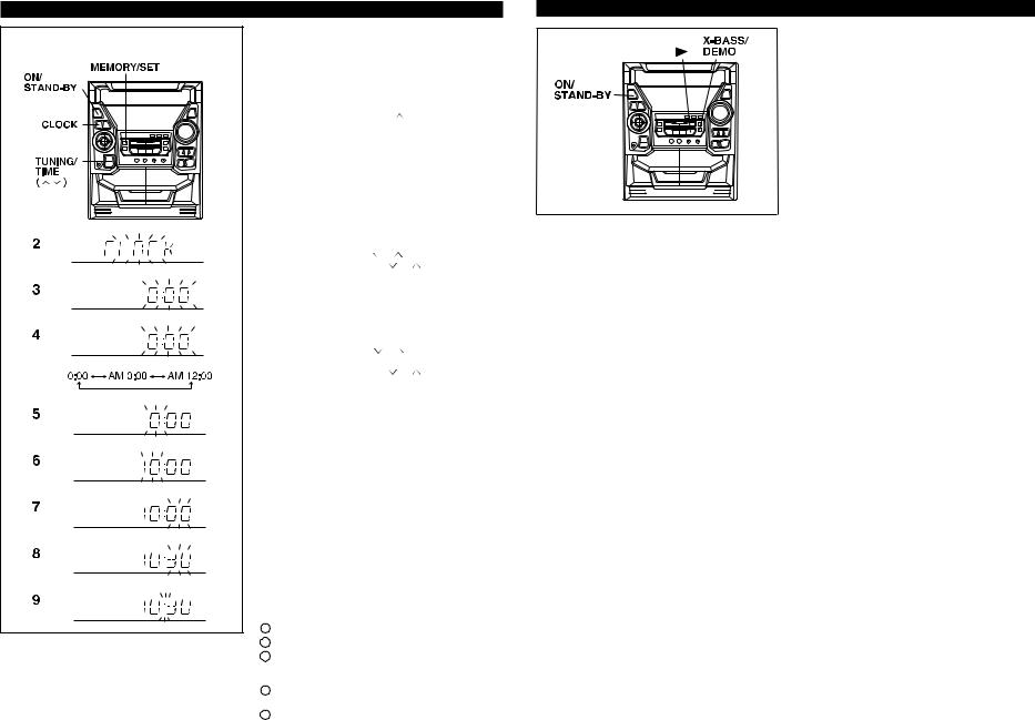
SETTING THE CLOCK
|
In this example, the clock is set for the 24-hour (0:00) system. |
||
(Main unit operation) |
1 Press the ON/STAND-BY button to enter the stand-by mode. |
||
|
|||
|
2 Press the CLOCK button. |
|
|
|
3 Within 5 seconds, press |
button. |
|
|
4 Press the TUNING/TIME |
) button to select the time |
|
|
display mode. |
|
|
|
“0:00” |
→The 24-hour display will appear. |
|
|
|
(0:00 - 23:59) |
|
|
“AM 0:00” →The 12-hour display will appear. |
||
|
|
(AM 0:00 - PM 11:59) |
|
|
“AM 12:00”→The 12-hour display will appear. |
||
|
|
(AM 12:00 - PM 11:59) |
|
|
● Note that this can only be set when the unit is first in- |
||
|
stalled or it has been reset. |
|
|
|
5 Press the MEMORY/SET |
|
|
|
6 Press the TUNING/TIME |
) button to adjust the hour. |
|
|
● Press the TUNING/TIME |
) button once to ad- |
|
|
vance the time by 1 hour. Hold it down to advance con- |
||
|
tinuously. |
|
|
|
● When the 12-hour display is selected, “AM” will chang |
||
|
automatically to “PM”. |
|
|
|
7 Press the MEMORY/SET |
|
|
|
8 Press the TUNING/TIME |
) button to adjust the min- |
|
|
utes. |
|
|
|
● Press the TUNING/TIME |
) button once to ad- |
|
|
vance the time by 1 minute. Hold it down to change the |
||
|
time in 5 minute intervals. |
|
|
|
● The hour setting will not advance even if minutes advance |
||
|
from “59” to “00”. |
|
|
|
9 Press the MEMORY/SET button. |
|
|
|
● The clock starts operating from “0” second. |
||
|
(Seconds are not displayed.) |
|
|
|
And then the clock display will disappear after a few sec- |
||
|
onds. |
|
|
|
To see the time display: |
|
|
|
Press the CLOCK button. |
|
|
|
● The time display will appear for about 5 seconds. |
||
|
Note: |
|
|
|
● The clock display will flash on and off at the push of the |
||
|
CLOCK button when the AC power supply is restored after |
||
|
a power failure occurs or after the AC power lead is discon- |
||
|
nected. |
|
|
|
If this happens, follow the procedure below to change the |
||
|
clock time. |
|
|
|
To change the clock time: |
|
|
|
1 Press the CLOCK button. |
|
|
Illustration:CD-DP2500W |
2 Within 5 seconds, press the MEMORY/SET button. |
||
3 Perform steps 6 - 9 above. |
|
||
|
|
||
|
To change the time display mode: |
||
|
1 Perform steps 1 - 2 in the section “RESETTING THE M |
||
|
CROCOMPUTER”. |
|
|
|
2 Perform steps 1 - 9 above. |
|
|
RESETTING THE MICROCOMPUTER
Reset the microcomputer under the following conditions:
● To erase all of the stored memory contents (clock and timer settings, and tuner and CD presets).
● If the display is not correct. ● If the operation is not correct.
1 Press the ON/STAND-BY button to enter the stand-by mode.
2 Whilst pressing down the 0button and the X-BASS/ DEMO button, hold down the ON/STAND-BY button for at least 1 second.
● “CLEAR AL” will appear.
Caution:
● The operation explained above will erase all data stored in memory including clock and timer settings, and tuner and CD presets.
Illustration:CD-DP2500W
MANUAL OPERATION
DP2500W/DK2500W-CD
CD-DP2500W/DK2500W
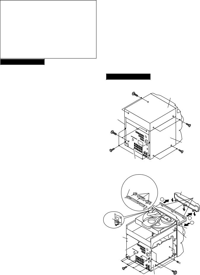
DISASSEMBLY
Caution on Disassembly
Follow the below-mentioned notes when disassembling the unit and reassembling it, to keep it safe and ensure excellent performance:
1.Take cassette tape and compact disc out of the unit.
2.Be sure to remove the power supply plug from the wall outlet before starting to disassemble the unit.
3.Take off nylon bands or wire holders where they need be removed when disassembling the unit. After servicing the unit, be sure to rearrange the leads where they were before disassembling.
4.Take suffcient care on static electricity of integrated circuits and other circuits when servicing.
CD-DP2500H/DK2500W
STEP |
REMOVAL |
|
PROCEDURE |
|
FIGURE |
|
|
|
|
|
|
1 |
Top Cabinet |
1. |
Screw ..................... |
(A1) x4 |
9-1 |
|
|
|
|
|
|
2 |
Side Panel |
1. |
Screw ..................... |
(B1) x8 |
9-1 |
|
(Left/right) |
|
|
|
|
|
|
|
|
|
|
3 |
CD Player Unit/ |
1. |
Turn on the power supply, |
9-2 |
|
|
CD Tray Cover |
|
open the disc tray, take out |
|
|
|
|
|
the CD cover, and close. |
|
|
|
|
|
(Note 1) |
|
|
|
|
2. |
Screw ..................... |
(C1) x1 |
|
|
|
3. |
Hook ....................... |
(C2) x3 |
|
|
|
4. |
Hook ....................... |
(C3) x2 |
|
|
|
5. |
Socket .................... |
(C4) x3 |
|
|
|
|
|
|
|
4 |
Rear Panel |
1. |
Screw ..................... |
(D1) x9 |
9-2 |
|
|
|
|
|
|
5 |
Main PWB |
1. |
Screw ..................... |
(E1) x3 |
9-2 |
|
|
2. |
Socket .................... |
(E2) x2 |
10-3 |
|
|
|
(CD-DP25000W) |
|
|
|
|
2. |
Socket .................... |
(E2) x3 |
|
|
|
|
(CD-DK25000W) |
|
|
|
|
3. |
Flat Cable .............. |
(E3) x1 |
|
|
|
4. |
Lug Wire ................. |
(E4) x1 |
|
|
|
5. |
Socket .................... |
(E5) x1 |
|
|
|
|
|
|
|
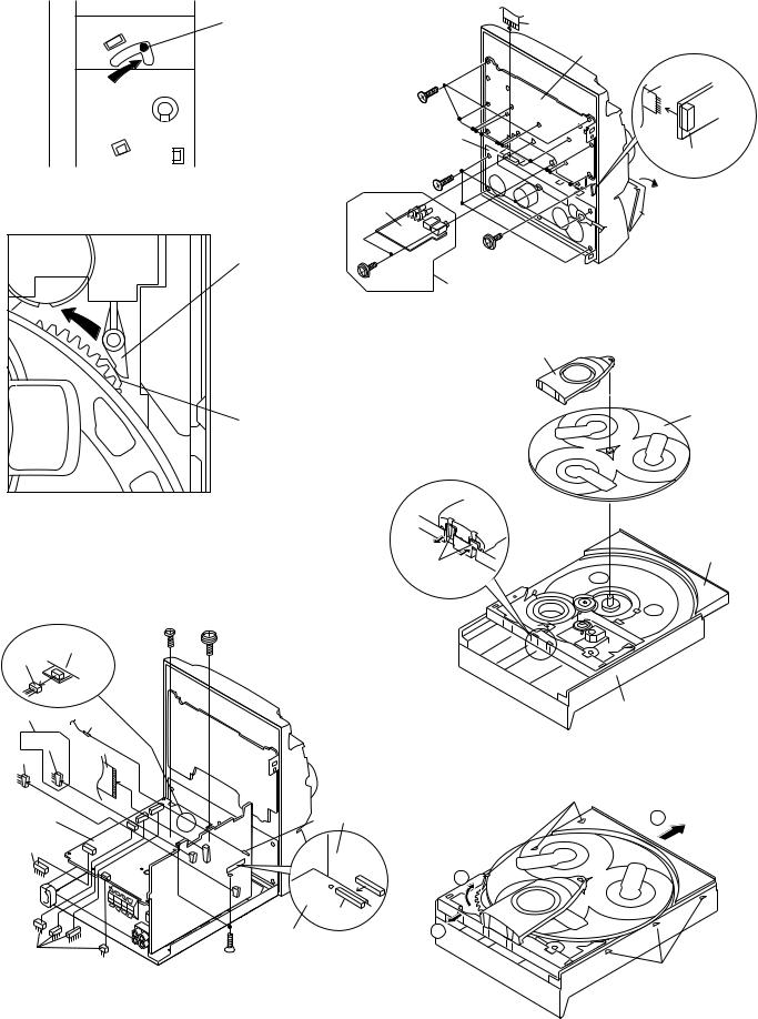
6 |
Power Supply PWB |
1. |
Screw ..................... |
(F1) x2 |
10-3 |
|
|
2. |
Socket .................... |
(F2) x5 |
|
|
|
3. |
Flat Wire ................. |
(F3) x1 |
10-4 |
|
|
|
|
|
|
7 |
Front Panel |
1. |
Screw ..................... |
(G1) x2 |
10-3 |
|
|
|
|
|
|
8 |
Karaoke PWB |
1. |
Screw ..................... |
(H1) x2 |
10-4 |
|
(CD-DK25000W |
|
|
|
|
|
ONLY) |
|
|
|
|
|
|
|
|
|
|
9 |
Display PWB/ |
1. Screw ..................... |
(J1) x15 |
10-4 |
|
|
Headphones PWB |
2. |
Flat Cable .............. |
(J2) x1 |
|
|
|
|
|
|
|
10 |
Tape Mechanism |
1. |
Open the cassette holder |
10-4 |
|
|
|
2. |
Screw ..................... |
(K1) x5 |
|
|
|
|
|
|
|
11 |
Turntable |
1. |
Hook ....................... |
(L1) x2 |
10-5 |
|
|
2. |
Cover ..................... |
(L2) x1 |
|
|
|
|
|
|
|
12 |
Disc Tray |
1. |
Turn fully the lock lever in the |
10-1 |
|
|
|
|
arrow direction. |
|
|
|
|
2. |
While holding the lock lever,rotate |
10-2 |
|
|
|
|
the cam gear until the cam gear |
|
|
|
|
|
rib engages with the clamp lever. |
|
|
|
|
3. |
Push the slide holder backward to |
10-6 |
|
|
|
|
engage the claw with the groove |
|
|
|
|
|
and remove it in the direction |
|
|
|
|
|
of the arrow. .............. |
(M1) x6 |
|
|
|
|
|
|
|
13 |
CD Servo PWB |
1. |
Screw ..................... |
(N1) x1 |
11-1 |
|
(Note 2) |
2. |
Hook ....................... |
(N2) x2 |
|
|
|
3. |
Socket .................... |
(N3) x4 |
|
|
|
|
|
|
|
14 |
CD Mechanism |
1. |
Hook ....................... |
(P1) x2 |
11-2 |
|
|
2. |
Hook ....................... |
(P2) x3 |
|
|
|
|
|
|
|
15 |
Loading Motor PWB |
1. |
Hook ....................... |
(Q1) x5 |
11-2 |
|
|
|
|
|
|
Note 1:
How to open the changer manually. (Fig. 10-1)
1.In this state, turn fully the lock lever in the arrow direction through the hole on the loading chassis bottom.
2.While holding the lock lever, rotate the cam gear anticlockwise until the cam gear rib engages with the clamp lever. (Fig. 10-2)
3.After that, push forward the CD slide holder.
Note 2:
1. After removing the connector for the optical pickup from the connector, wrap the conductive aluminium foil around the front end of the connector so as to protect the optical pickup from electrostatic damage.
Note 3:
1.Be careful not to break the claw of the CD mechanism.
2.When fining back the cam gear assembly, let it lock by front movement.
CD-DP2500H/DK2500W
(A1)x2
Top Cabinet
ø3x12mm
Side Panel (Right)
(B1)x2 |
|
|
ø3x10mm |
|
(A1)x2 |
|
|
ø3x12mm |
|
|
Side Panel |
|
|
(Left) |
(B1)x4 |
|
(B1)x2 |
ø3x10mm |
Rear |
ø3x10mm |
|
|
|
|
Panel |
|
Figure 9-1
CD Servo
PWB
(C4)x3 |
DC Tray Cover |
(C2) x3
1
(C3) x1 |
1 |
|
|
Pull |
2 |
CD Player
Unit
Rear |
(C3)x1 |
Panel |
(C1)x1 ø3x10mm
(E1)x3  ø3x10mm
(D1)x7 |
|
ø3x10mm |
(D1)x2 |
|
|
|
Main PWB ø3x10mm |
Figure 9-2
– 9 –
CD-DP2500W/DK2500W
LOCK LEVER |
(J2)x1 |
|
|
Display PWB |
|
(J1)x14 |
(F3)x1 |
|
ø3x10mm |
||
Tape |
|
|
Mechanism |
||
(K1)x5 |
Headphones |
|
PWB |
||
ø3x10mm |
||
Open |
||
Figure 10-1 |
||
|
||
Karaoke |
Cassette |
|
PWB |
||
|
Holder |
|
CLAMP LEVER |
(J1)x1 |
|
(H1)x1 |
ø3x10mm |
|
|
||
ø3x10mm |
CD-DK2500W |
|
ONLY
Figure 10-4
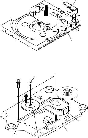
(L2) x1
Turntable
CAM GEAR RIB
Figure 10-2
Disc Tray
|
|
|
|
(L1) x2 |
|
Tape |
|
(F1)x1 |
(F1)x1 |
|
|
ø3x6mm |
||
|
Mechanism |
|||
(E5)x1 |
|
ø3x10mm |
||
|
|
|
||
CD-DK2500W |
|
|
CD Player Unit |
|
ONLY |
|
(E4)x1 |
|
|
(E2)x1
(E3)x1
(E2)x1
Figure 10-5
(M1) x3
Power
Supply Main PWB 3 PWB
(F2)x1
2
|
|
|
(E2)x1 |
|
|
Power |
1 |
(F2)x4 |
(G1)x2 |
Supply |
|
PWB |
|
ø3x10mm |
(M1) x3 |
|
Figure 10-3 Figure 10-6
– 10 –
(N1)x1 |
CD Servo |
CD Player |
|
ø3x8mm |
|||
Base |
|||
PWB |
|||
|
|
||
|
(N3) x2 |
|
(N2) x2
(N3) x2
Figure 11-1
CP-DP2500
STEP |
REMOVAL |
|
PROCEDURE |
|
FIGURE |
|
|
|
|
|
|
1 |
Front Panel |
1. Front Panel ............ |
(A1) x1 |
11-3 |
|
|
|
|
|
|
|
2 |
Woofer |
1. Screw ..................... |
(B1) x4 |
11-3 |
|
|
|
|
|
|
|
4 |
Tweeter |
1. |
Screw .................... |
(C1) x2 |
11-3 |
|
|
|
|
|
|
5 |
Super Tweeter |
1. |
Screw .................... |
(D1) x2 |
11-3 |
|
|
|
|
|
|
CD-DP2500W/DK2500W
CD |
(P2) x3 |
|
Mechanism |
|
|
|
|
Loading |
|
(P1) x1 |
Motor |
(P1) x1 |
PWB |
(Q1) x5
Figure 11-2
CP-DP2500
(A1)x1
(D1)x2
Ø3x10mm
(C1)x2 |
Ø3x10mm |
(B1)x4
Ø4x12mm
Woofer
Screw Driver
Figure 11-3
– 11 –
CD-DP2500W/DK2500W
REMOVING AND REINSTALLING THE MAIN PARTS
TAPE MECHANISM SECTION
Perform steps 1 to 7 and 10 of the disassembly method to remove the tape mechanism.
How to remove the record/playback and erase heads (TAPE 2) (See Fig. 12-1)
1.When you remove the screw (A1) x 2 pcs., the recording/ playback head and three-dimensional head of the erasing head can be removesd.
How to remove the playback head (TAPE 1) (See Fig. 12-2)
1.When you remove the screw (B1) x 2 pcs., the playback head.
How to remove the pinch roller (TAPE 1/2) (See Fig. 12-3)
1. Carefully push the inside claw to remove it. The pinch roller pawl in the direction of the arrow <A>, and remove the pinch roller (C1) x 1 pc., in the direction of the arrow <B>.
Note:
When installing the pinch roller, pay attention to the spring mounting position.
How to remove the belt (TAPE 1) (See Fig. 12-4)
1.Remove the main belt (D1) x 1 pc., from the motor side.
2.Remove the FF/REW belt (D2) x 1 pc.
TAPE 2
Record/Playback
Head
Erase Head
(A1)x2 |
Ø2 x 5mm |
Figure 12-1
TAPE 1
Playback
Head
(B1)x2 Ø2 x 9mm
Figure 12-2
How to remove the belt (TAPE 2) (See Fig. 12-4)
1.Remove the main belt (E1) x 1 pc., from the motor side.
2.Remove the FF/REW belt (E2) x 1 pc.
How to remove the motor (See Fig. 12-5)
1. Remove the screws (F1) x 2 pcs., to remove the motor.
|
|
Pinch Roller |
|
|
|
Pawl |
|
|
Pinch Roller |
<A> |
|
|
(C1)x1 |
|
|
|
<B> |
|
|
|
|
Figure 12-3 |
|
Motor |
|
Motor |
|
TAPE2 |
FF/REW |
Motor |
TAPE1 |
|
|||
|
Belt |
TAPE2 |
Main Belt |
|
(E2)x1 |
(D1)x1 |
|
|
Main Belt |
||
|
|
|
|
|
|
(E1)x1 |
|
(F1) x2 |
|
|
|
Ø 2.6 x 5mm |
|
|
|
|
|
|
TAPE1 |
|
Main Belt |
|
FF/REW |
|
|
|
Belt |
|
|
|
(D2)x1 |
Figure 12-5 |
Figure 12-4 |
– 12 –
CD-DP2500W/DK2500W
CD MECHANISM SECTION
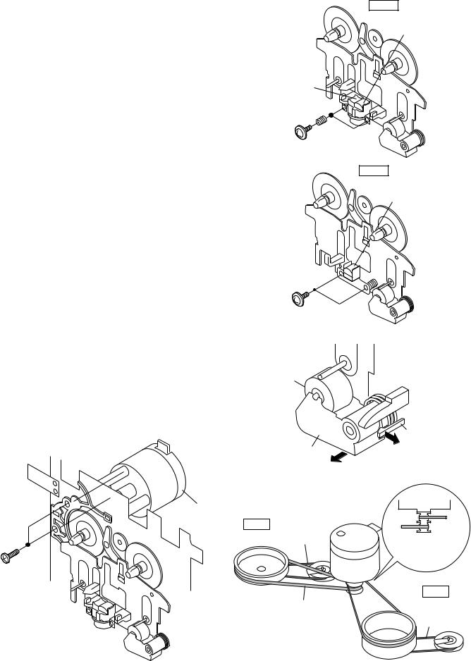
Perform steps 1, 2, 3, and 11 to 14 of the disassembly method to remove the CD mechanism.
How to remove the loading motor (See Fig. 13-1)
1. Bend the hooks (A1) x 5 pcs., to remove the loading motor.
Loading Motor
(A1)x1
(A1)x2
How to remove the pickup (See Fig. 13-2)
1.Remove the stop washer (B1) x 1 pc., to remove the gear (B2).
2.Remove the screws (B3) x 2 pcs., to remove the shaft (B4).
3.Remove the pickup.
Note
After removing the connector for the optical pickup from the connector wrap the conductive aluminium foil around the front end of connector so as to protect the optical pickup from electrostatic damage.
(A1)x2
CD Base
|
Figure 13-1 |
|
(B1) x2 |
Stop Washer |
|
(B3) x1 |
||
ø2.6 x6mm |
||
|
Pickup
Shaft |
CD Mechanism |
|
Gear |
||
(B2) x1 |
||
(B4) x1 |
||
|
||
|
Figure 13-2 |
TEST MODE
During POWER OFF mode,push below each 2 keys [ON/STAND-BY] key.
Then go to each TEST MODE.
KEY |
TEST MODE |
CONTENTS |
|
|
|
[ON/STAND-BY] [TUNER] + [X-BASS] |
TEST 1 |
TUNER PRESET MEMORY CLEAR |
|
|
|
[ON/STAND-BY] [MEMORY/SET] + [X-BASS] |
TEST 2 |
TUNER PRESET FOR PRODUCTION |
|
|
|
[ON/STAND-BY] [>>] + [X-BASS] |
TEST 3 |
KEY AND DISPLAY TEST |
|
|
|
[ON/STAND-BY] [CD] + [X-BASS] |
TEST 4 |
CD TEST MODE |
|
|
|
[ON/STAND-BY] [TAPE] + [X-BASS] |
TEST 5 |
TAPE TEST MODE |
|
|
|
[ON/STAND-BY] [>] + [X-BASS] |
TEST 6 |
ALL CLEAR(RESET) |
|
|
|
[ON/STAND-BY] [TUN UP] + [X-BASS] |
TEST 7 |
AUDIO TEST |
|
|
|
[ON/STAND-BY] [TUN DOWN] + [X-BASS] |
TEST 8 |
PRODUCTION INITIALIZE FOR CHANGER |
|
|
|
– 13 –
CD-DP2500W/DK2500W
ADJUSTMENT
MECHANISM SECTION
• Driving Force Check
Torque Meter |
Specified Value |
|
|
Play: TW-2111 |
Tape 1: Over 80 g |
|
Tape 2: Over 80 g |
|
|
• Torque Check
Torque Meter |
Specified Value |
|
|
|
|
|
Tape 1 |
Tape 2 |
|
|
|
Play: TW-2111 |
30 to 80 g. cm |
30 to 80 g.cm |
|
|
|
Fast forward: TW-2231 |
— |
70 to 180 g.cm |
|
|
|
Rewind: TW-2231 |
— |
70 to 180 g.cm |
|
|
|
TUNER SECTION
fL: Low-range frequency fH: High-renge frequency
• AM IF/RF
Signal generator: 400 Hz, 30%, AM modulated
Test Stage |
Frequency |
Frequency |
Setting/ |
Instrument |
|
|
Display |
Adjusting |
Connection |
|
|
|
Parts |
|
|
|
|
|
|
AM IF |
450 kHz |
1,602 kHz |
T351 |
*1 |
|
|
|
|
|
AM Band |
— |
531 kHz |
(fL): T306 |
*2 |
Coverage |
|
|
1.1 ± 0.1 V |
|
|
|
|
|
|
AM Tracking |
990 kHz |
990 kHz |
(fL): T303 |
*1 |
|
|
|
|
|
*1. Input: Antenna,SO301 Output: TP302
*2. Input: Antenna,SO301 Output: TP301
CD SECTION
•Adjustment
Since this CD system incorporates the following automatic adjustment functions, readjustment is not needed when replacing the pickup. Therefore, different PWBs and pickups can be combined freely.
Each time a disc is changed, these adjustments are performed automatically. Therefore, playback of each disc can be performed under optimum conditions.
Items adjusted automatically
(1)Offset adjustment (The offset voltage between the head amplifier output and the VREF reference voltage is compensated inside the IC.)
*Focus offset adjustment
*Tracking offset adjustment
(2)Tracking balance adjustment (waveform drawing 14-3 EFBL)
(3)Gain adjustment (The gain is compensated inside the IC so that the loop gain at the gain crossover frequency will be 0dB.)
*Focus gain adjustment
*Tracking gain adjustment
• Tape Speed
|
|
|
Test Tape |
|
|
Adjusting |
|
Specified |
Instrument |
||||||||||||||||
|
|
|
|
|
|
|
|
|
|
|
|
Point |
|
|
|
Value |
Connection |
||||||||
|
|
|
|
|
|
|
|
|
|
|
|
|
|
||||||||||||
Normal |
|
|
MTT-111 |
|
|
Variable |
|
3,000 ± |
|
|
Speaker |
||||||||||||||
speed |
|
|
|
|
|
|
|
|
|
Resistor in |
|
30 Hz |
terminal |
||||||||||||
|
|
|
|
|
|
|
|
|
|
motor. |
|
|
|
|
|
|
|
(Load |
|||||||
|
|
|
|
|
|
|
|
|
|
(MM1) |
|
|
|
|
|
|
|
resistance: |
|||||||
|
|
|
|
|
|
|
|
|
|
|
|
|
|
|
|
|
|
|
|
|
|
|
|
|
6 ohms) |
|
|
|
|
|
|
|
|
|
|
|
|
|
|
|
|
||||||||||
|
|
|
|
|
|
|
|
|
|
|
|||||||||||||||
|
|
|
|
|
|
|
|
|
TAPE MECHANISM |
|
|
|
|
|
|
||||||||||
|
|
|
|
|
|
|
|
|
|
|
|
|
|
|
|
|
|
|
|
|
|
|
|
|
|
|
|
|
|
|
|
|
|
|
|
|
|
|
|
|
|
|
|
|
Motor |
|
|||||
|
|
|
|
|
|
|
Variable Resistor in motor |
|
|||||||||||||||||
|
|
|
|
|
|
|
|
|
|
|
|
|
|
|
|
|
|
||||||||
|
|
|
|
|
|
|
|
|
|
Figure 14-1 |
|
|
|
|
|
|
|
||||||||
|
|
|
|
|
|
|
|
|
|
|
|
|
|
|
|
|
|
|
|
|
|
|
|
||
|
|
|
|
|
|
|
|
|
|
|
|
|
|
MAIN PWB |
|
|
|
|
|||||||
|
|
|
|
|
|
|
|
|
|
|
|
|
|
|
|
|
|
|
|
|
|
|
|
|
|
|
|
|
|
|
|
|
|
|
IC302 |
|
|
|
|
|
|
|
|
SO301 |
|
||||||
|
|
|
|
|
|
|
|
|
|
|
|
|
|
|
|
|
|
|
|
|
|
|
|||
|
|
|
|
|
|
|
|
|
|
|
|
|
|
|
C375 |
|
|
|
FM75 ohms |
||||||
|
|
|
|
|
|
|
|
|
|
|
|
|
|
|
|
|
|
||||||||
|
|
|
|
|
AM IF |
|
|
|
|
C393 |
|
|
|
|
|
|
|
|
|||||||
|
|
|
|
|
T351 |
|
|
|
|
TP301 |
|
|
|
|
|
|
|
|
|
|
|
|
|||
|
|
|
|
|
|
|
T301 |
|
|
|
|
|
|
|
|
|
|
|
|
||||||
|
|
|
|
|
|
|
|
|
|
|
|
|
|
|
|
|
|
GND |
|
||||||
|
|
|
|
|
|
CF352 |
|
|
|
|
|
|
|
|
|
|
|
|
|||||||
|
|
|
|
|
|
|
|
|
|
|
|
|
T302 |
|
|
|
|
|
|
|
|
|
|
||
|
|
|
|
|
|
|
|
|
|
|
|
CNP301 |
|
||||||||||||
|
|
|
|
|
|
|
|
|
|
|
|
|
|
|
|
|
|
|
|
||||||
|
|
|
CF351 |
|
|
|
|
|
|
|
|
|
|
|
|
|
|
AM LOOP |
|||||||
|
|
|
|
|
|
|
|
|
|
|
|
|
|
|
|
|
IC301 |
|
|
|
ANTENNA |
||||
|
|
|
|
IC303 |
|
CF302 |
|
|
|
|
|
|
|
|
|
|
|
|
|||||||
|
|
R357 |
|
|
|
|
|
L312 |
|
|
|
|
|
|
|
||||||||||
|
|
|
|
|
|
|
|
|
|
|
|
|
|
|
|
|
|
|
|
||||||
|
|
|
|
|
|
|
|
|
T303 |
|
|
|
|
|
|
|
|||||||||
|
|
|
|
TP302 |
|
|
|
|
|
|
|
|
AM Tracking |
|
|
|
|
|
|
|
|
||||
|
|
|
|
|
|
|
|
|
|
|
|
|
|
|
|
|
|
|
|
|
|
|
|
||
|
|
|
|
|
|
|
|
|
|
T306 |
|
|
|
|
|
|
|
|
|
|
|
|
|||
|
|
|
|
|
|
|
|
|
AM Band Coverage |
|
|
|
|
|
|
|
|
|
|
|
|||||
|
|
|
Figure 14-2 ADJUSTMENT POINT |
|
|||||||||||||||||||||
CD ERROR CODE DESCRIPTION |
|
||||||||||||||||||||||||
|
|
|
|
|
|
|
|
|
|
|
|
|
|
|
|
|
|
|
|
|
|
|
|
|
|
Error |
|
|
|
|
|
|
|
|
|
|
|
|
|
|
State Code |
|
|||||||||
|
|
|
|
|
|
|
|
|
|
|
|
|
|
|
|
|
|
|
|
|
|
|
|
|
|
|
|
[Servo System Error] |
|
|
|
|
|
|
|
||||||||||||||||
0001 |
|
Cannot detect Pickup-in SW |
|
|
|
|
|
|
|
||||||||||||||||
0002 |
|
DSP access error |
|
|
|
|
|
|
|
|
|
|
|
|
|||||||||||
|
|
|
|
|
|
|
|
|
|
|
|
|
|
|
|
|
|
|
|
|
|
|
|
|
|
|
|
[Error during close operation] |
|
||||||||||||||||||||||
0101 |
|
Open/Close SW not functioning (Low → High) |
|||||||||||||||||||||||
0103 |
|
Open/Close SW not functioning (High → Low) |
|||||||||||||||||||||||
|
|
[Error during open operation] |
|
|
|
|
|
|
|
||||||||||||||||
0201 |
|
Open/Close SW not functioning (Low → High) |
|||||||||||||||||||||||
0203 |
|
Open/Close SW not functioning (High → Low) |
|||||||||||||||||||||||
|
|
[Error during skip operation] |
|
|
|
|
|
|
|
||||||||||||||||
0302 |
|
Pickup-in SW is not detected |
|
|
|
|
|
|
|
||||||||||||||||
0306 |
|
During Disc 1 search, Open/Close SW or Clamp SW |
|||||||||||||||||||||||
|
|
or Disc SW do not change to low. |
|
||||||||||||||||||||||
0307 |
|
Clamp SW not function (Low → High) |
|
||||||||||||||||||||||
0308 |
|
Clamp SW not function (High → Low) |
|
||||||||||||||||||||||
|
Stopped |
T |
|
|
|
|
|
1999/04/05 |
20:26:47 |
|
|
|
|
|
|
|
|||
|
CH1=500mV |
CH2=200mV |
CH3=1V |
|
|
500ms/div |
|||
|
DC |
10:1 |
DC |
10:1 |
DC 10:1 |
|
|
(500ms/div) |
|
|
|
|
|
|
|
|
|
NORM:20kS/s |
|
T |
FDO |
|
|
|
|
|
|
|
|
|
|
|
|
|
|
|
|
|
|
1 |
|
|
|
|
|
|
|
|
|
3 |
TE |
|
|
|
|
|
|
|
|
|
|
|
|
|
|
|
|
|
|
|
EFBL |
|
|
|
|
|
|
|
|
2 |
|
|
|
|
|
|
|
|
|
|
|
|
|
|
|
|
|
|
CH2 |
|
|
|
|
|
|
|
|
|
v/DIV |
|
|
|
|
|
|
|
|
|
200mV |
|
=Filter= |
|
=Offset= |
=Record Length= |
|
=Trigger= |
|||
Smoothing : ON |
CH1 : |
0.000V |
Main : |
100K |
Mode : SINGLE |
||||
BW |
: FULL |
|
CH2 : |
0.000V |
Zoom : |
2k |
Type |
: EDGE CH1 |
|
|
|
|
CH3 : |
0.00V |
|
|
Delay : |
0.0ns |
|
|
|
|
CH4 : |
0.00V |
|
|
Hold off : |
0.2us |
|
|
|
|
|
Figure 14-3 |
|
|
|||
– 14 –

CD-DP2500W/DK2500W
EXPLANATION OF DOLBY SURROUND PRO LOGIC AND EVALUATION METHOD
Outline
•Namely, two speakers are connected in parallel to one amplifier.
•In the Pro Logic BYPASS mode the amplifier for C-ch (center channel) and the amplifier for S-ch (surround channel) are in MUTE state. The SP output is cut.
•In the normal mode of Pro Logic ON mode the amplifiers for C-ch and S-ch are in operative state, so that the SP output appears.
•In the Phantom mode of Pro Logic ON mode the amplifier for C-ch is in MUTE state, so that the SP output is cut. The amplifier for S-ch (surround) is in operative state, so that the SP output appears
•State of element output and terminal output in specific mode
|
State of set |
Dolby Pro Logic |
|
Dolby Pro Logic On mode |
|
|
|||
Output point |
Bypass mode |
Normal mode |
|
Phantom mode |
|||||
IC501 |
1 pin L-out |
Output enabled state |
|
Output enabled state |
|
Output enabled state |
|||
|
2 pin R-out |
Output enabled state |
|
Output enabled state |
|
Output enabled state |
|||
|
|
|
|
|
|
|
|
|
|
IC501 |
3pin C-out |
No output |
|
Output enabled state |
|
No output |
|||
IC501 |
9pin S-out |
No output |
|
Output enabled state |
|
Output enabled state |
|||
SP OUT |
L-ch |
Output enabled state |
|
Output enabled state |
|
Output enabled state |
|||
(SO901) |
R-ch |
Output enabled state |
|
Output enabled state |
|
Output enabled state |
|||
SP OUT C-ch |
No output in MUTE (Q501) state |
Output enabled state |
|
No output in MUTE (Q501) state |
|||||
(SO901) |
|
|
|
|
|
|
|
|
|
SP OUT S-ch |
No output in MUTE (Q502) state |
Output enabled state |
|
Output enabled state |
|||||
(SO901) |
|
|
|
|
|
|
|
|
|
|
|
|
|
|
|
|
|
|
|
Test tone output |
|
|
|
|
|
|
|
|
|
|
|
|
Output point |
Phantom mode |
|||||
• Pro Logic ON Normal mode |
|
|
|||||||
|
|
|
|
|
|
|
|||
Press the remote control TEST TONE button. |
|
SP out |
|
L-ch |
Input signal is output. |
||||
→Output of only L-ch →Output of only C-ch |
|
(SO901) |
|
R-ch |
Input signal is output. |
|
|||
↑ |
|
|
↓ |
|
|
|
|
|
|
|
|
|
(SO901) SP out C-ch |
SP cut, no output |
|||||
Output of only S-ch ← Output of only R-ch |
|
|
|
|
|
|
|||
|
(SO901) SP out S-ch |
Almost no output (only omitting component) |
|||||||
The test tone (noise) is repeatedly output for output period |
|
||||||||
|
|
|
|
|
|
||||
|
(2) L-ch/R-ch reverse phase input into VIDEO IN input jack in |
||||||||
(2 sec). |
|
|
|
|
|||||
In this case the following indication appears repeatedly. |
|
VIDEO Function mode |
|||||||
→TEST →L-ch →C-ch |
|
|
(Reverse phase: Phase difference between L and R is 180°) |
||||||
|
↑ |
↓ |
|
|
|
|
|
|
|
|
|
|
Output point |
Normal mode |
|||||
|
S-ch ← R-ch |
|
|
||||||
|
|
|
|
|
|
|
|
||
|
|
|
SP out |
|
L-ch |
Almost no output (only omitting component) |
|||
• Pro Logic ON Phantom mode |
|
|
|
||||||
|
|
|
|
|
|
|
|||
|
|
(SO901) |
|
R-ch |
Almost no output (only omitting component) |
||||
Press the remote control TEST TONE button. |
|
|
|||||||
|
|
|
|
|
|
||||
|
(SO901) SP out C-ch |
Almost no output (only omitting component) |
|||||||
→Output of only L-ch →Output of only R-ch |
|
||||||||
|
|
↑ |
↓ |
|
(SO901) SP out S-ch |
Input signal is output. |
|||
|
|
← Output of only S-ch |
|
|
|
|
|
|
|
|
|
|
|
|
|
|
|
||
The test tone (noise) is repeatedly output for output period |
|
Output point |
Phantom mode |
||||||
(2 sec). |
|
|
|
|
|
|
|
|
|
|
|
|
|
SP out |
|
L-ch |
Almost no output (only omitting component) |
||
|
|
|
|
|
|
||||
|
|
|
|
|
|
|
|
|
|
In this case the following indication appears repeatedly. |
|
(SO901) |
|
R-ch |
Almost no output (only omitting component) |
||||
|
|
|
|
|
|
||||
|
(SO901) SP out C-ch |
SP cut, no output |
|||||||
→TEST → L-ch → R-ch |
|
|
|||||||
|
|
|
|
|
|
|
|||
|
|
|
|
|
|
|
|||
|
↑ |
↓ |
|
|
(SO901) SP out S-ch |
Input signal is output. |
|||
|
← S-ch← |
|
• Accordingly, if you want to output signal waveform to C-ch SP |
||||||
Relation between VIDEO IN input and output in Pro Logic |
out, give the same phase input into L-ch/R-ch INPUT in the |
|
Pro Logic Normal mode. |
||
ON state |
||
If one of channels receives input, C-ch does not output. Only |
||
(1) L-ch/R-ch same phase input into VIDEO IN input jack in |
||
L-ch or R-ch outputs. |
||
VIDEO Function mode |
||
|
Output point |
Normal mode |
|
|
|
|
SP out |
L-ch |
Almost no output (only omitting component) |
(SO901) |
R-ch |
Almost no output (only omitting component) |
|
|
|
(SO901) SP out C-ch |
Input signal is output. |
|
|
|
|
(SO901) SP out S-ch |
Almost no output (only omitting component) |
|
|
|
|
•If you want to output signal waveform to S-ch SP out, you can use either Normal mode or Phantom mode. However, 180° reverse phase input must be given to L-ch/R-ch INPUT.
– 15 –
CD-DP2500W/DK2500W
NOTES ON SCHEMATIC DIAGRAM
•Resistor:
To differentiate the units of resistors, such symbol as K and M are used: the symbol K means 1000 ohm and the symbol M means 1000 kohm and the resistor without any symbol is ohm-type resistor. Besides, the one with “Fusible” is a fuse type.
•Capacitor:
To indicate the unit of capacitor, a symbol P is used: this symbol P means micro-micro-farad and the unit of the capacitor without such a symbol is microfarad. As to electrolytic capacitor, the expression “capacitance/withstand voltage” is used.
(CH), (TH), (RH), (UJ): Temperature compensation (ML): Mylar type
(P.P.): Polypropylene type
•Schematic diagram and Wiring Side of P.W.Board for this model are subject to change for improvement without prior notice.
•The indicated voltage in each section is the one measured by Digital Multimeter between such a section and the chassis with no signal given.
1.In the tuner section, ( ) indicates AM
< > indicates FM stereo
2.In the main section, a tape is being played back.
3.In the deck section, a tape is being played back. ( ) indicates the record state.
4.In the power section, a tape is being played back.
5.In the CD section, the CD is stopped.
•Parts marked with “ ” (
” ( 


 ) are important for maintaining the safety of the set. Be sure to replace these parts with specified ones for maintaining the safety and performance of the set.
REF. NO |
DESCRIPTION |
POSITION |
|
|
|
SW1 |
OPEN/CLOSE |
ON—OFF |
|
|
|
SW2 |
CLAMP |
ON—OFF |
|
|
|
SW3 |
DISC NUMBER |
ON—OFF |
|
|
|
SW4 |
PICKUP IN |
ON—OFF |
|
|
|
SW701 |
CD |
ON—OFF |
|
|
|
SW702 |
TAPE |
ON—OFF |
|
|
|
SW703 |
TUNING DOWN |
ON—OFF |
|
|
|
SW704 |
MEMORY/SET |
ON—OFF |
|
|
|
SW705 |
REV |
ON—OFF |
|
|
|
SW706 |
FF |
ON—OFF |
|
|
|
SW707 |
PLAY |
ON—OFF |
|
|
|
SW708 |
STOP |
ON—OFF |
|
|
|
SW710 |
REC |
ON—OFF |
|
|
|
SW711 |
TUNING UP |
ON—OFF |
|
|
|
SW712 |
VIDEO |
ON—OFF |
|
|
|
REF. NO |
DESCRIPTION |
POSITION |
|
|
|
SW713 |
TUNING |
ON—OFF |
|
|
|
SW714 |
DIMMER |
ON—OFF |
|
|
|
SW715 |
X-BASS |
ON—OFF |
|
|
|
SW716 |
EQUAL |
ON—OFF |
|
|
|
SW717 |
NORMAL |
ON—OFF |
|
|
|
SW718 |
PHANTOM |
ON—OFF |
|
|
|
SW719 |
BY-PASS |
ON—OFF |
|
|
|
SW720 |
ON/STAND-BY |
ON—OFF |
|
|
|
SW721 |
CLOCK |
ON—OFF |
|
|
|
SW722 |
TIMER |
ON—OFF |
|
|
|
SW728 |
DISC 1 |
ON—OFF |
|
|
|
SW729 |
DISC 2 |
ON—OFF |
|
|
|
SW730 |
DISC 3 |
ON—OFF |
|
|
|
SW731 |
DISC SKIP |
ON—OFF |
|
|
|
SW732 |
OPEN/CLOSE |
ON—OFF |
|
|
|
|
FRONT |
|
|
|
|
|
|
|
|
|
|
FRONT |
||||||||||
|
|
|
VIEW |
|
|
|
|
|
|
|
|
|
|
|||||||||
|
|
|
|
|
|
|
|
|
|
FRONT |
|
|
VIEW |
|||||||||
|
|
|
|
|
|
|
|
|
|
|
VIEW |
|
|
|
|
|
|
|||||
|
|
|
|
|
|
|
|
|
|
|
|
|
|
|
|
|
|
|
|
|
|
|
|
|
|
|
|
|
|
|
|
|
|
|
|
|
|
|
|
|
|
|
|
|
|
|
|
E |
C B |
|
|
|
|
|
|
|
|
|
|
|
|
|
||||||
|
(S) (G) (D) |
|
|
|
|
|
|
|
|
|
|
|
|
|
||||||||
|
|
|
|
|
|
|
|
|
|
|
|
|
|
|||||||||
(1) |
(2) (3) |
|
|
|
|
|
|
|
|
|
|
|
|
|
|
|||||||
|
B C E |
|
|
|
|
|
||||||||||||||||
KTA1266 GR |
|
|
KTA1273 Y |
|
|
|
|
|
||||||||||||||
|
|
KTD2026 Y |
|
|
|
|
|
|||||||||||||||
KRC102 M |
|
|
KTC3203 Y |
4204SRT7 |
||||||||||||||||||
|
|
|
|
|
|
|
|
|
|
|||||||||||||
KRC104 M |
|
|
KTC3199 GR |
|
|
|
|
|
|
|
|
4204UYT7 |
||||||||||
KTA1271 Y |
|
|
KTC107 M |
|
|
|
|
|
|
|
|
|
|
|
|
|
||||||
KTA1274 Y |
|
|
2SC3203 Y |
|
|
|
|
|
|
|
|
|
|
|
|
|
||||||
|
|
|
|
|
|
KTC3194 Y |
|
|
|
|
|
|
|
|
|
|
|
|
|
|||
Figure 20 TYPES OF TRANSISTOR AND LED
– 16 –
CD-DP2500W/DK2500W
|
CD DIGITAL OUT |
|
|
|
|
|
|
||
|
|
IC99 |
|
|
TO MAIN SECTION |
|
|
||
|
|
|
|
|
(TO IC601) |
|
|
||
CNS99 |
1 |
2 |
3 |
CH-R |
AGND |
CH-L |
DGND |
+B6(+5V) |
|
|
|
|
|
|
|
|
|||
CNP5 |
1 |
2 |
3 |
1 |
2 |
3 |
4 |
5 |
CNP11 |
|
|
||||||||
Q2
|
|
|
TO DISPLAY SECTION |
|
|
|
|
||||
CDINT |
WRQ |
DRF |
CE |
DO |
DI |
CLK |
CD RES |
CLAMP SW |
GND |
CNP12 |
|
1 |
2 |
3 |
4 |
5 |
6 |
7 |
8 |
9 |
10 |
||
|
|||||||||||
SW1 |
|
SW2 |
SW3 |
|
|
|
OPEN/ |
CLAMP |
DISC |
|
|
|
|
CLOSE |
|
|
NUMBER |
|
|
|
|
|
|
|
|
M |
M3 |
|
|
|
|
|
T/T |
|
|
|
|
|
|
UP/DOWN |
|
|
|
|
|
|
|
MOTOR |
|
|
|
+ |
|
- |
|
1 |
2 |
3 |
4 |
5 |
6 |
BI4 |
1 |
2 |
3 |
4 |
5 |
6 |
CNS4 |
|
||||||
1 |
2 |
3 |
4 |
5 |
6 |
CNP4 |
|
||||||
|
37 |
75 |
76 |
|
|
45 |
46 |
47 |
48 |
32 |
31 |
30 |
|
|
65 |
CE |
DOUT |
CONT6 |
CONT7 |
|
|
LCHO |
LVSS |
RVSS |
RCHO |
CONT4 |
CONT3 |
CONT2 |
74 |
|
|
|
|
|
|
|
|
|
|
|
|
|||
|
|
|
|
|
|
|
|
|
|
|
|
|
|
|
66 |
CL |
|
|
|
|
|
|
|
|
|
|
|
|
64 |
67 |
DI |
|
|
|
|
|
|
|
|
|
|
|
|
40 |
68 |
DO |
|
|
|
|
|
|
|
|
|
|
|
|
19 |
69 |
INT |
|
|
|
|
|
|
IC2 |
|
|
|
|
|
13 |
|
|
|
|
|
|
|
|
|
|
|
|
|||
|
|
|
|
|
|
|
|
|
|
|
|
|
3 |
|
70 |
WRQ |
|
|
|
|
LC78641E |
|
|
|
|
||||
|
|
|
|
|
|
|
|
|
||||||
|
|
|
|
|
|
SERVO/SIGNAL |
|
|
|
|
||||
71 |
RES |
|
|
|
|
CONTROL |
|
|
|
CONT5 |
33 |
|||
72 |
DEF |
|
|
|
|
|
|
|
|
|
|
SLD0 |
26 |
|
|
|
|
|
|
|
|
|
|
|
|
|
|
||
52 |
XOUT |
|
|
|
|
|
|
|
|
|
|
SPD0 |
25 |
|
XL1 |
|
|
|
|
|
|
|
|
|
|
|
|
|
24 |
16.9344MHz |
|
|
VVDD |
ADAVDD |
VDD |
LVDD |
RVDD |
XVDD |
|
HFL |
RFEV |
FE |
FD0 |
|
51 |
VDD5V |
|
TE |
|
||||||||||
XIN |
|
|
|
|
|
|
|
|
|
|
TD0 |
23 |
||
|
73 |
|
5 |
18 |
36 |
44 |
49 |
50 |
|
7 |
14 |
15 |
16 |
|
|
+5V |
|
|
|
+3.3V |
|
|
|
|
|
|
|
|
|
|
|
|
|
|
|
|
|
|
|
|
|
|
|
|
1 |
2 |
17 |
25 |
41 |
42 |
38 |
39 |
|
CONSTANT |
Q1 |
|
|
|
17 |
18 |
19 |
20 |
21 |
22 |
|
|
|
|
|
|
|
|
|
|
|
|
|
VOLTAGE |
|
|
|
|
HFL |
TE |
TE- |
FE |
FE- |
RFEV |
|
|
|
|
|
|
|
|
|
|
|
|
|
|
|
|
|
|
|
|
|
18 |
VCC1 |
|
|
|
IC3 |
|
|
|
|
||||||
|
|
|
|
|
|
|
|
|
|
|
|
|
|
|
|
|
|
|
|
|
|||
|
|
|
|
|
|
|
|
|
|
|
|
|
|
|
|
|
|
|
|
|
|
|
|
+3.3V |
30 |
|
|
|
|
|
|
|
|
|
|
|
|
40 |
VCC4 |
|
|
M63001FP |
|
|
|
||
|
|
|
|
|
|
|
|
|
|
|
|
|
|
|
|
|
FOCUS/TRACKING/ |
|
|
||||
|
|
|
|
|
|
IC1 |
|
|
|
|
|
|
|
24 |
VCC2 |
|
SPIN/SLIDE DRIVER |
|
|||||
|
|
|
|
|
|
|
|
|
|
|
|
+5V |
|
|
|
|
|
|
|
|
|
|
|
|
|
|
|
|
LA9235M |
|
|
|
LASER |
|
23 |
|
|
|
|
|
|
|
|
|
|||
|
23 |
|
|
|
|
|
|
|
|
|
|
|
|
|
|
|
|
|
|||||
|
|
|
|
SERVO AMP. |
|
|
|
DRIVER |
|
|
|
|
|
|
|
|
|
|
|
|
|||
|
11 |
|
|
|
|
|
|
|
|
|
Q3 |
|
|
28 |
VCC3 |
|
|
|
|
|
|
|
|
|
|
|
|
|
|
|
|
|
|
+3.3V |
|
|
|
|
|
|
|
|
|
|
|
||
|
9 |
FIN1 |
FIN2 |
TIN1 |
TIN2 |
|
|
LDD |
|
|
|
|
|
|
4 |
5 |
6 |
7 |
|
15 |
16 |
26 |
27 |
|
|
|
PD |
|
|
|
|
|
|
|
|
|
|
|
|
|
|
|
|||||
|
|
1 |
2 |
3 |
4 |
|
7 |
8 |
|
|
|
|
|
|
|
|
|
|
|
|
|
|
|
|
+5V |
|
|
|
|
|
|
|
|
|
|
|
|
|
|
|
|
|
|
|
|
|
|
|
|
|
|
|
|
|
|
|
|
|
|
M1 |
M |
|
|
|
|
|
|
|
|
|
|
|
|
|
|
|
|
|
|
|
|
|
|
SPINDLE |
|
|
|
|
|
|
|
|
|
|
|
PICKUPUNIT |
|
|
|
|
|
|
|
|
|
FOCUSCOIL |
TRACKINGCOIL |
MOTOR |
|
|
|
|
|
|
|
|
|
|
|
|
|
|
|
|
|
|
|
|
M2 |
M |
|
|
|
|
|
|
|
|
|
|
|||
|
|
|
|
|
|
|
|
|
|
|
|
SLED |
|
|
|
|
|
|
|
|
|
|
|
MOTOR
35
29
22
21
14
8
SW4
PICKUP IN
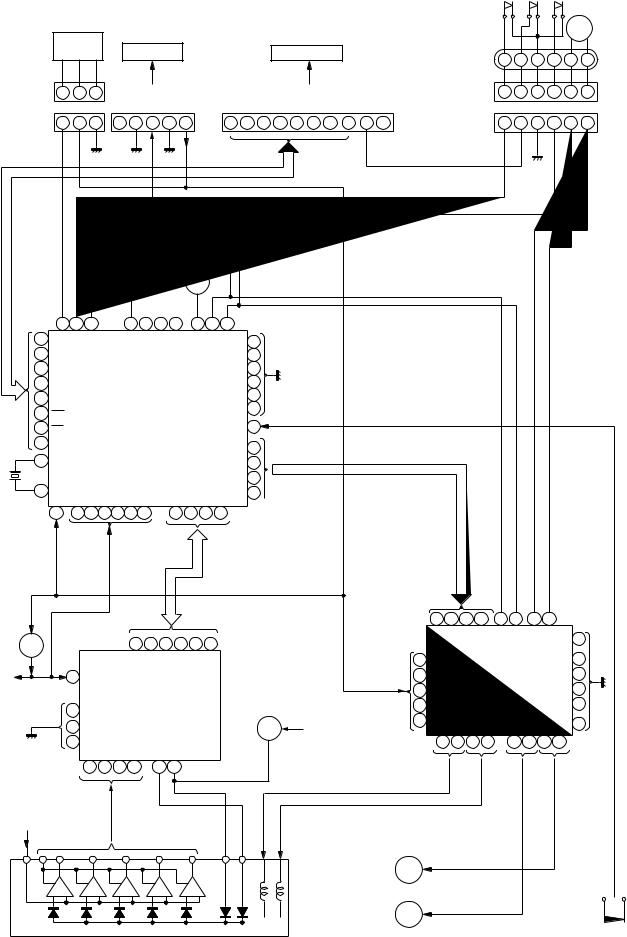
Figure 21 BLOCK DIAGRAM (1/3)
– 17 –
CD-DP2500W/DK2500W
|
|
|
|
IC301 |
|
|
|
|
|
|
|
|
|
||
|
|
FM FRONT END |
|
|
|
|
|
|
|
||||||
SO301 |
1 |
2 |
3 |
4 |
5 |
6 |
7 |
8 |
9 |
|
|
|
|
|
|
FM ANTENNA |
|
|
|
|
|
|
|
|
FM IF |
FM IF |
|
|
|
|
|
|
|
|
|
|
|
|
|
|
+B9 |
|
|
|
|
||
FM 75Ω |
BF301 |
|
|
|
|
|
|
|
|
CF303 |
|
|
+B9 |
|
|
|
|
|
|
|
|
|
T302 |
|
|
|
|
||||
|
|
|
|
|
|
|
|
|
|
|
|
||||
GND |
FM B.P.F. |
|
|
|
|
|
|
|
|
|
|
|
|
|
|
|
|
|
|
|
|
|
|
|
|
|
|
|
|
|
|
|
|
|
|
|
|
|
|
|
Q302 |
|
AM IF |
|
|
|
|
|
|
|
|
|
|
|
|
|
|
|
|
|
|
|
|
|
FM RF |
|
FM OSC |
|
|
|
FM IF IN |
T351 |
CF352 |
|
|
MONO/ST |
|||
|
|
|
|
OSC BUFFER |
|
|
|
|
|||||||
|
|
|
|
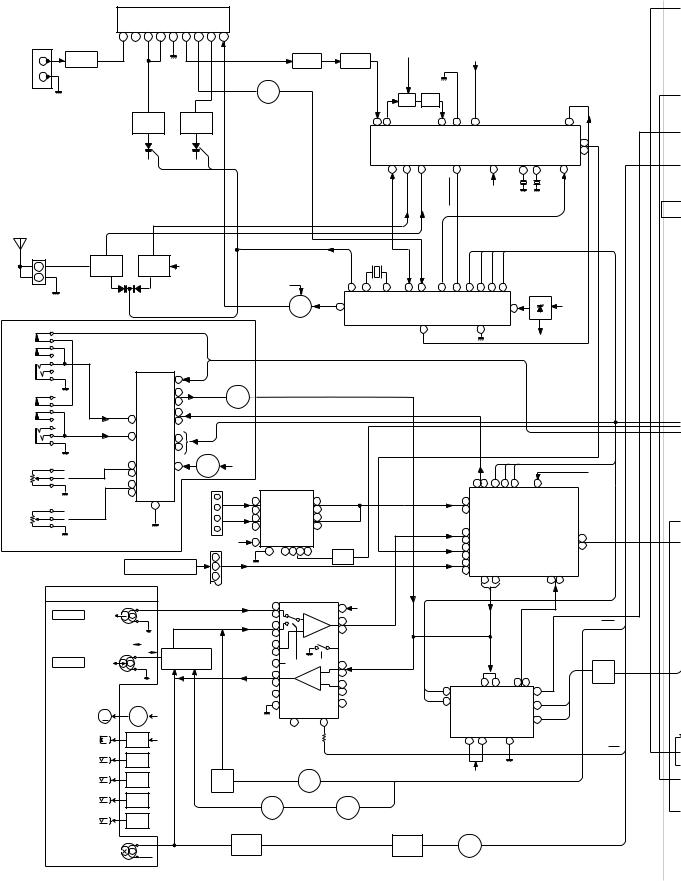
|
|
|
FM+B |
|
|||||||
|
|
|
|
|
|
|
|
|
|
|
|
|
|
||
|
|
|
|
|
|
|
|
|
|
|
|
|
|
|
|
|
|
|
L312 |
|
|
T301 |
|
|
1 |
2 |
4 |
5 |
9 |
13 |
|
|
|
|
|
|
|
|
|
|
|
|
AM MIX |
AM IF GND VCC |
MO/ST |
||
|
|
|
|
|
|
|
|
IC303 |
|
|
|
|
|
|
|
|
L 14 |
|
|
|
|
|
|
|
|
|
LA1832 |
|
|
|
|
|
|
|
R 15 |
||
|
|
|
|
|
|
|
FM/AM IF MPX. |
|
|
|
|
|
|
FM/AM |
||||
|
|
|
|
|
|
|
24 |
23 |
21 |
|
7 |
|
|
9 |
FMDET |
8 |
17 |
12 |
|
|
|
|
|
|
|
OSCAMIN |
OSCAMIN |
RFAMIN |
|
STEREO |
|
+B9 |
CF351 |
X351 |
456KHz |
||
|
|
|
|
|
|
|
|
|
|
|
|
|
|
|
|
|
||
AM LOOP |
|
|
|
|
|
|
|
|
|
|
|
|
|
|
|
|
|
|
ANTENNA |
|
|
|
|
|
|
|
|
|
|
|
|
|
|
|
|
|
|
CNP301 |
AM ANT. |
AM OSC |
|
|
|
|
|
|
|
|
|
|
|
|
|
|
|
|
|
|
|
|
|
|
X352 |
IN |
IN |
|
|
|
|
|
|
|
|
|
|
1 |
T303 |
T306 |
+B9 |
|
4.5MHz |
|
|
|
|
|
|
|
|
|
||||
|
|
FM |
|
|
|
|
|
|
|
|
|
|||||||
|
|
|
AM |
|
|
CE |
|
|
DO |
|
|
|
||||||
2 |
|
|
|
+B5 |
|
|
|
|
|
DI |
CL |
VOLTAGE |
||||||
|
|
|
|
20 |
1 |
22 |
15 |
16 |
9 |
11 |
3 |
4 |
5 |
6 |
||||
|
|
|
|
|
|
OSC |
IC302 |
|
|
|
|
|
|
REGURATER |
||||
|
|
|
|
FM +B |
|
|
|
|
|
|
|
|
|
|
||||
|
|
|
|
|
|
|
|
|
|
|
|
|
|
|
|
|||
|
|
|
|
Q360 |
7 FM |
|
|
LC72131 |
|
|
|
|
17 |
|
|
+B5 |
||
|
|
|
|
VOLTAGE |
|
|
PLL (TUNER) |
|
|
|
|
|
|
|
||||
|
|
|
|
|
|
|
|
10 |
|
|
|
21 |
|
|
|
|
|
|
|
|
|
|
REGULATOR |
|
|
|
|
|
|
|
|
|
|
|
|
||
|
|
|
ICK1 |
|
|
|
|
|
|
|
|
|
|
|
|
|
+B9 |
|
JK1 |
|
|
|
|
|
|
|
|
|
|
|
|
|
|
|
|
|
|
|
M65856P |
|
|
|
|
|
|
|
|
|
|
|
|
|
|
|
||
MIC 1 |
|
|
|
|
|
|
|
|
|
|
|
|
|
|
|
|
||
|
KARAOKE |
|
|
|
|
|
|
|
|
|
|
|
|
|
|
|
||
|
|
|
|
|
|
|
|
|
|
|
|
|
|
|
|
|
||
|
|
|
LATCH 40 |
|
|
|
|
|
|
|
|
|
|
|
|
|
|
|
|
|
|
ROUT 35 |
QK2,3 |
|
|
|
|
|
|
|
|
|
|
|
|
|
|
|
|
|
LOUT 36 |
|
|
|
|
|
|
|
|
|
|
|
|
|
|
|
|
|
|
|
|
|
|
|
|
|
|
|
|
|
|
|
|
|
|
JK 2 |
|
MIC1 IN |
LIN 31 |
|
|
|
|
|
|
|
|
|
|
|
|
|
|
|
MIC 2 |
|
4 |
RIN 32 |
|
|
|
|
|
|
|
|
|
|
|
|
|
|
|
|
|
MIC2 IN |
|
|
|
|
|
|
|
|
|
|
|
|
|
|
|
|
9CLOCK 41 DATA 42
|
|
7 |
VCC 23 |
QK1 |
|
|
+B5 |
IC201 |
|
|
|
|
|
|
|
|
|
|
|
+B5 |
||
VRK 2 |
|
8 |
|
|
|
|
|
BU4066BC |
|
|
|
|
|
|
|
|
|
|
|
|||
|
|
|
|
|
|
|
|
|
|
|
|
|
|
|
|
|
|
|||||
MIC 2 |
|
12 |
|
|
|
|
|
SWITCHING |
|
|
|
|
8 17 |
24 |
1 |
2 |
23 |
|
|
|||
LEVEL |
|
|
|
|
|
|
|
|
|
|
|
|
||||||||||
|
13 |
|
L |
|
|
|
|
|
|
|
|
|
|
|
|
CL |
DI |
CE |
|
|
|
|
|
|
|
|
|
|
|
1 |
|
|
2 |
|
|
VIDEO |
L 9 |
|
|
|
|
||||
|
|
22 |
R |
|
|
|
|
|
|
|
|
|
|
|
|
|
|
|||||
VRK 1 |
|
|
|
|
3 |
|
|
9 |
|
|
|
R 16 |
|
|
|
|
|
|
|
|||
|
|
|
|
|
|
|
|
|
|
|
|
|
|
|
|
|
|
|
||||
|
|
|
L |
|
|
|
8 |
|
|
4 |
|
|
|
|
|
|
|
IC401 |
|
|
||
MIC 1 |
|
|
|
|
|
|
|
|
|
|
|
|
|
|
|
|
|
|||||
|
|
|
|
|
|
|
10 |
|
|
11 |
|
|
|
|
|
|
|
|
|
|||
LEVEL |
|
|
|
R |
|
|
|
|
|
|
|
TAPE |
L 10 |
|
|
LC75341 |
|
|
||||
|
|
|
|
|
|
|
|
|
|
|
|
|
|
|
|
|||||||
|
|
|
JK201 |
|
|
|
|
|
|
|
|
|
|
|
21 R |
|||||||
|
|
|
|
|
|
|
|
|
|
|
|
|
|
R 15 |
|
|
|
|
|
|||
CD-DK2500W ONLY |
|
|
VIDEO IN |
+B5 |
14 |
|
|
|
|
|
TUNER |
AUDIO PROCESSOR 4 |
L |
|||||||||
|
|
|
6 12 5 13 |
|
|
|
L 11 |
|||||||||||||||
|
|
|
|
|
1 |
|
7 |
|
|
Q403 |
|
|
R 14 |
|
|
|
|
|
|
|
||
|
|
FROM CD SECTION |
|
|
|
|
|
Q404 |
|
CD |
L 12 |
|
|
|
|
|
|
|
||||
|
|
2 |
|
|
|
|
|
|
|
|
|
|
|
|
|
|||||||
|
|
CNP11 |
|
|
|
|
|
IC101 |
|
|
|
R 13 |
|
|
|
|
|
|
|
|||
|
|
|
|
3 |
|
|
|
|
|
|
|
|
|
|
|
|
|
|||||
|
|
|
|
|
|
|
|
|
|
|
|
|
|
|
|
|
|
|
||||
|
|
|
|
|
|
|
|
|
|
AN7345K |
|
|
|
|
17 |
8 |
|
|
7 |
18 |
|
|
TAPE MECHANISM Ass'y |
|
CNS401 |
|
PLAYBACK AND RECORD |
|
|
|
|
|
|
|
|
|
|||||||||
|
|
|
|
|
/PLAYBACK AMP. |
|
|
|
|
|
|
|
|
|
|
|||||||
|
L-CH |
|
|
|
|
|
|
L(T1) |
1 |
|
|
13 |
+B5 |
|
|
|
|
|
|
|
|
|
TAPE 1 |
|
|
|
|
|
|
R(T1) 24 |
|
P.B. |
|
|
|
|
|
|
|
|
|
||||
|
|
|
|
|
|
|
|
|
|
|
|
|
|
|
|
|
|
|||||
PB HEAD |
R-CH |
|
|
|
|
|
|
L(T2) |
2 |
|
|
4 L |
PB |
|
|
|
|
|
|
|
|
REC |
|
|
|
|
|
|
|
|
|
21 R |
|
|
|
|
|
|
|
|
|
||||
|
|
|
|
|
|
|
|
R(T2) 23 |
|
|
|
|
|
|
|
|
|
|
|
|
||
|
|
REC |
SWITCHING |
|
L NF 3 |
|
|
|
|
|
|
|
|
|
|
|
|
|
||||
|
L-CH |
P.B |
Q103~Q106 |
|
|
|
R NF 4 |
|
|
|
|
|
|
|
|
|
|
|
|
|
||
TAPE 2 |
|
|
POP REDUCE 6 |
T1/T2 |
H/N |
7 |
L REC |
|
|
|
|
|
|
|
|
|
||||||
R-CH |
|
|
|
|
|
|
|
|
|
|
|
|
Q501 |
|||||||||
|
|
|
|
|
|
|
|
|
|
|
|
|
|
|
|
|
|
|
||||
REC/PB HEAD |
|
|
|
|
|
|
L REC 9 |
REC |
|
18 |
R |
|
|
L 74 |
|
|
|
|
|
Q502 |
||
|
|
AC BIAS |
|
|
|
|
R REC 16 |
|
|
8 L NF |
|
|
75 R |
2 |
1 |
|
|
|||||
|
|
|
|
|
|
REF 14 |
|
|
17 R NF |
34 |
|
|
|
|
|
24 |
|
|
||||
|
|
MOTOR |
|
|
|
|
|
|
|
IC501 |
|
|
|
|
|
|||||||
|
|
DRIVER |
|
|
|
|
|
|
12 |
NOR/ |
|
10 ALC |
38 |
|
|
|
9 |
|
|
|||
MM1 |
|
|
|
|
|
|
|
|
T1/T2 |
|
|
|
M62464AFP |
|
|
|
|
|||||
TAPE |
M |
Q706 |
+B4 |
|
|
|
|
|
|
HIGH |
|
|
|
DOLBY PRO LOGIC |
3 |
|
|
|||||
MOTOR |
|
|
|
|
|
|
|
|
|
15 |
19 |
|
|
|
DECORD |
|
|
|
|
|
||
|
|
|
|
|
|
|
|
|
|
|
|
|
|
|
|
|
|
|||||
SOLM1,SOLM2 |
Q704 |
+B4 |
|
|
|
|
|
|
|
|
|
|
|
21 |
69 |
|
25 |
|
|
|
||
SOLENOID |
|
Q705 |
|
|
|
|
|
|
|
|
|
|
|
|
|
|
|
|||||
|
|
|
|
|
|
|
|
|
|
|
|
|
|
|
|
|
|
|
|
T1/T2 |
||
SWM2 |
|
IC701 |
|
|
|
|
|
|
|
|
|
|
|
|
|
|
|
|
|
|
|
|
|
|
|
|
|
|
|
|
|
|
|
|
|
|
|
|
|
|
|
|
|
||
T2 PLAY |
|
54PIN |
|
|
|
SWITCHING |
|
SWITCHING |
|
|
|
|
|
|
|
|
|
|
|
|||
SWM1 |
|
IC701 |
|
|
|
Q107 |
|
|
|
Q111 |
|
|
|
+B5 |
|
|
|
|
|
|
||
T1 PLAY |
|
53PIN |
|
|
|
Q108 |
|
|
|
|
|
|
|
|
|
|
|
|
|
|
||
|
|
|
|
|
|
|
|
|
|
|
|
|
|
|
|
|
|
|
|
|||
SWM4 |
|
IC701 |
|
|
|
|
|
|
|
|
|
|
|
|
|
|
|
|
|
|
|
|
R. PLAY |
|
56PIN |
|
|
|
|
|
Q109 |
|
|
Q110 |
|
|
|
|
|
|
|
|
|
||
|
|
|
|
|
|
|
|
SWITCHING |
|
|
|
|
|
|
|
|
|
|||||
SWM3 |
|
IC701 |
|
|
|
|
|
|
|
|
|
|
|
|
|
|
|
|
|
|
||
|
|
|
|
|
|
|
|
|
|
|
|
|
|
|
|
|
|
|
|
|
||
F. PLAY |
|
55PIN |
|
|
|
|
|
|
|
|
|
|
|
SWITCHING |
BAIS |
|
|
|
|
|
|
|
|
|
|
|
|
|
BIAS |
|
|
|
|
|
|
|
|
|
|
|
|
|
|||
|
|
|
|
|
|
|
|
|
|
|
|
|
|
|
|
|
|
|
|
|
|
|
|
ERASE |
|
|
|
|
OCS |
|
Q128 |
|
|
|
|
|
Q124 |
Q126 |
|
|
|
|
|
BAIS |
|
|
|
|
|
|
|
|
L104 |
|
|
|
|
|
|
|
|
|
|
|
||||
|
HEAD |
|
|
|
|
|
|
|
|
|
|
|
|
|
|
|
|
|
|
|
|
|
Figure 22 BLOCK DIAGRAM (2/3)
– 18 –
TAP MECHA
Z
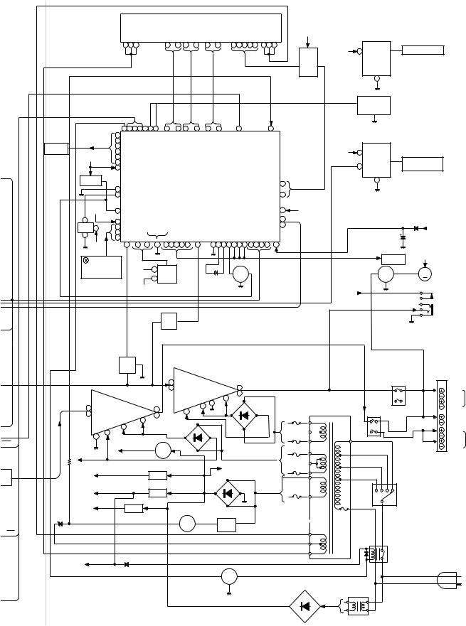
CD-DP2500W/DK2500W
FL701
DISPLAY
+B7
1 2 3 |
6 ~ 14 33 ~ 53 |
27 ~ 32 |
15 16 24 25 26 |
54 55 56 |
+B7 |
|
|
|
|
|
|
|
Q701 |
18 |
IC702 |
LED711~LED717 |
|
|
|
|
|
Q702 |
|
|
|
|
|
|
|
|
|
|
BU2092F |
|
|
|
|
|
|
Q703 |
|
|
|
|
|
|
|
|
|
|
|
|
|
|
|
|
|
Q710 |
|
|
|
|
|
|
|
|
Q711 |
|
|
|
|
|
|
|
|
Q712 |
|
|
|
|
|
|
|
|
|
|
|
17 |
|
|
|
|
|
|
|
|
VOLUME |
|
|
|
|
|
|
|
|
VR701 |
|
|
92 ~100 60 ~ 78 |
80 ~ 85 |
REQ |
|
|
|
|
|
47 52 53 5455 3738 |
6 |
79 |
|
|
|
|
|
50 |
|
|
|
|
|
51 |
|
|
|
|
TAPE |
53 |
|
|
|
|
MECHANISM |
54 |
|
|
|
|
+B7 |
55 |
|
|
|
|
56 |
|
|
|
|
|
|
|
|
|
|
|
RESET |
46 |
VDD |
|
IC701 |
|
|
|
|
|
||
IC704 |
|
|
|
IX0334AW |
|
KIA7042P |
|
|
|
||
|
SYSTEM MICROCOMPUTER |
||||
|
40 |
||||
|
39 |
|
|
|
|
+B7 |
36 |
|
|
|
VDD |
1 |
34 |
AVDD |
|
|
LATCH |
|
|
|
MIC IN |
||
RX701 3 |
33 |
|
|
SMUTE |
|
|
|
VDD |
|||
2 |
31 |
|
|
||
|
32 |
|
|
|
|
+B7 |
|
2 27 ~ 30 |
25 |
20 19 1817 15 41 |
13 12 11 10 9 8 7 24 23 22 21 1 |
KEY |
|
|
|
|
|
SW701~SW713 |
–B1 |
4 |
IC601 |
|
|
SW714~SW722 |
|
||||
SW728~SW733 |
|
|
IC602 |
Q709 |
|
|
|
|
8 |
IC603 |
XL701 |
|
|
+B4 |
KIA4558P |
|
|
|
|
|
OPE AMP. |
|
|
+B7 |
18 |
IC703 |
|
|
|
BU2092F |
LED701~LED710 |
|
|
|
|
|
12 |
|
LED718 |
|
|
17 |
|
86
~
91
16 +B7
57
58
|
+B7 |
|
MEMORY |
|
BACK UP |
TO CD |
+B6 |
SECTION |
|
Q910 |
M FANM901MOTOR |
+B3
|
|
|
|
|
|
|
Q503 |
|
|
|
|
|
|
|
|
JK601 |
|
|
|
|
|
|
|
|
Q504 |
|
|
|
|
|
|
|
|
HEADPHONES |
|
5 |
|
|
|
|
|
|
|
|
|
|
|
|
|
|
|
|
|
|
|
|
|
|
Q401 |
|
|
|
|
|
|
|
|
|
|
|
|
|
|
|
|
|
Q402 |
|
|
|
|
|
|
|
|
|
|
|
|
|
|
|
|
|
|
|
L |
IC901 |
|
|
|
FRONT |
|
|
|
RL902 |
|
|
|
|
|
|
|
|
1 |
STK40271 |
|
|
|
|
|
|
|||
|
|
|
|
|
|
|
15 |
|
7 |
L-OUT |
|
|
|
|
|
||
|
|
|
|
|
|
|
R |
POWER AMP. |
10 |
R-OUT |
|
|
|
L-ch |
Front |
||
|
|
|
L |
IC902 |
|
|
|
+B1 |
4 |
|
|
|
PT801 |
|
|
||
|
|
|
|
|
L |
13 |
|
D801 |
|
POWER |
|
R-ch |
Speaker |
||||
|
|
|
1 |
STK40203 |
|
–B1 |
8 |
|
|
TRONSFORMER |
|
|
|||||
|
|
|
|
7 |
|
|
|
|
|
|
|||||||
|
|
|
15 |
POWER AMP. |
|
10 |
9 |
|
|
|
|
F801 |
(MAIN) |
RL901 |
|
|
|
|
|
|
|
|
|
|
|
|
|
|
Center |
||||||
|
|
|
R |
|
+B2 |
4 |
R |
|
|
|
|
|
T5A L 250V |
|
|
|
|
|
|
|
|
–B2 |
|
|
|
|
|
|
|
|
|
Speaker |
|||
|
|
|
|
8 |
|
|
D802 |
|
|
|
|
|
|
|
L-ch |
|
|
|
|
|
|
9 |
|
|
|
|
|
|
|
|
F802 |
|
|
Rear |
|
|
|
|
|
13 |
|
|
|
|
|
|
|
|
T5A L 250V |
|
|
|
|
REC |
|
|
|
|
|
|
|
|
|
|
|
|
F803 |
|
230-240V |
R-ch |
Speaker |
|
|
|
|
+B4(M+10V) |
Q823 |
|
|
|
|
|
|
|
|||||
|
|
|
|
|
|
|
|
|
|
T4A L 250V |
|
220V |
|
|
|||
|
|
–B3(–15V) |
|
|
|
|
|
|
|
|
SO901 |
|
|||||
|
|
|
|
|
|
|
|
|
|
|
|
|
|
||||
|
|
|
|
|
|
|
|
|
|
|
|
|
F804 |
|
127V |
Speaker Terminal |
|
|
|
|
|
|
|
KIA7810AP |
VOLTAGE |
|
+B3 |
|
|
|
|
|
|||
|
|
|
|
|
|
|
|
|
T4A L 250V |
|
|
|
|
||||
|
|
|
|
(A+10V) |
|
|
REGULATOR |
|
|
|
|
|
|
||||
501 |
|
|
+B5 |
|
|
|
|
|
|
|
110V |
|
|
||||
|
|
|
|
IC802 |
|
|
|
|
|
|
|
|
|
||||
|
|
|
|
|
|
|
|
|
|
|
|
|
|
||||
502 |
|
|
|
|
|
|
|
VOLTAGE |
|
|
D803 |
|
|
|
|
|
|
|
VROAD |
|
|
|
KIA7805AP |
|
|
|
|
|
|
|
|||||
|
|
|
(CD+5V) |
|
|
|
REGULATOR |
|
~D806 |
F805 |
|
|
|
|
|||
|
|
|
+B6 |
|
|
IC801 |
|
|
|
|
|
T2A L 250V |
|
|
|
|
|
|
|
|
|
|
|
|
|
|
|
|
|
|
|
|
|||
|
|
(UNSW+5V) |
AN78L05 |
|
|
|
|
|
|
|
T.F |
|
SW801 |
|
|||
|
|
IC804 |
|
|
VOLTAGE |
|
|
|
|
|
|
VOLTAGE |
|
||||
|
|
|
+B2 |
|
|
|
|
|
|
|
|
|
|
SELECTOR |
|
||
|
|
|
|
|
|
|
REGULATOR |
|
|
|
|
|
|
|
|||
|
ZD801 |
|
|
|
|
|
|
Q804 |
|
D807 |
|
|
|
|
|
|
|
|
|
|
|
|
|
|
|
|
|
|
|
|
|
|
|
||
|
|
|
|
|
|
|
|
|
~D809 |
|
|
|
|
|
|
|
|
T1/T2 |
|
|
|
|
|
|
|
|
|
D818 |
|
|
VF1 |
|
|
|
|
|
|
|
|
|
|
|
|
|
|
|
|
|
|
|
|
|
|
|
|
|
|
|
|
|
|
|
|
|
|
|
VF2 |
|
|
RL801 |
|
|
|
|
|
|
|
|
|
|
|
|
|
|
|
|
|
|
|
|
|
+B8 |
(SW+5V) |
|
|
|
|
|
|
|
|
|
|
|
AC POWER |
|
|
|
|
|
|
|
|
|
|
|
|
|
|
|
|
|
|
||
|
|
|
|
|
|
|
|
|
|
|
|
|
|
|
|
SUPPLY CORD |
|
|
|
|
|
|
|
|
|
|
|
Q803 |
|
|
|
|
|
|
|
BAIS |
|
|
|
|
|
|
|
|
|
|
|
|
|
|
|
AC 110/127/220/230-240V, |
|
|
|
|
|
|
|
|
|
|
|
|
|
|
|
|
50/60Hz |
|
|
|
|
|
|
|
|
|
|
|
|
|
|
|
|
|
PT802 |
|
|
|
|
|
|
|
|
|
|
|
|
|
|
|
D814~D817 |
|
POWER |
|
|
|
|
|
|
|
|
|
|
|
|
|
|
|
TRONSFORMER |
|
|
||
Figure 23 BLOCK DIAGRAM (3/3)
– 19 –

CD-DP2500W/DK2500W
A
B |
Vcc |
7 |
Vref |
6 |
|
|
E |
5 |
|
A |
|
|
4 |
|
|
|
|
|
B |
3 |
|
F |
|
|
2 |
|
|
|
|
|
C |
1 |
|
|
C
D
E
|
|
TR- |
1 |
|
TR+ |
|
|
|
TR+ |
2 |
|
|
|
||
|
|
|
|
|
FO+ |
FO+ |
3 |
|
|
|
|
|
|
FO- |
4 |
|
|
|
|
|
|
GND |
5 |
|
FO- |
|
|
F |
|
6 |
|
TR- |
PD |
||
|
|
VR |
7 |
|
ACTUATOR |
LD |
8 |
|
|
||
|
|
|
PICKUP UNIT(306)
G
CD MOTOR PWB-D
|
|
CNP3A |
|
M1 |
+ |
6 |
|
SPINDLE |
M |
||
|
|||
MOTOR |
5 |
||
|
- |
||
|
|
||
M2 |
+ |
4 |
|
SLED |
M |
3 |
|
MOTOR |
- |
||
SW4 |
|
2 |
|
|
|
||
PICKUP IN |
|
1 |
H
CD SERVO PWB-C
CNS1B |
CNS1A |
|
|
|
|
|
|
|
|
|
|
|
|
|
|
|
|
|
|
|
|
|
|
|
8 |
|
|
|
|
|
|
+B |
|
|
|
|
|
|
|
|
|
|
|
|
|
|
|
|
|
||
7 |
7 |
7 |
|
|
|
|
|
R50 |
|
|
|
|
|
|
|
|
|
|
|
|
|
|
|
|
|
|
|
|
|
|
47 |
|
|
|
|
|
|
|
|
|
|
|
|
|
|
|
|
|
|||
6 |
6 |
6 |
|
|
|
|
TIN1 |
|
|
|
|
|
|
|
|
|
|
|
|
|
|
|
|
|
|
5 |
5 |
5 |
R51 |
68K |
|
|
|
|
|
|
|
|
|
|
|
|
|
|
|
|
|
|
|
|
|
|
|
|
|
FIN1 |
|
|
|
|
|
|
|
|
|
|
|
|
|
|
|
|
|
|
|||
4 |
4 |
4 |
R52 |
68K |
|
|
|
|
|
|
|
|
|
|
|
|
|
|
|
|
|
|
C23 |
R12 |
|
|
|
|
|
|
|
|
|
|
|
|
|
|
|
|
|
|
|
|
|
|
|||||
3 |
3 |
3 |
R53 |
68K |
|
|
FIN2 |
|
|
|
|
|
|
|
|
|
|
|
|
|
|
|
|
0.047 |
680 |
|
|
|
|
|
|
|
|
|
|
|
|
|
|
|
|
|
|
|
|
||||||
|
|
|
|
TIN2 |
|
|
|
|
|
|
|
|
|
|
|
|
|
|
|
|
|
|
|||
2 |
2 |
2 |
R54 |
68K |
|
|
|
|
|
|
IC1 |
|
|
|
|
|
|
|
|
|
|
|
R79 |
||
|
|
|
|
|
|
|
|
|
|
|
|
|
|
|
|
|
|
|
|
1.5M |
|||||
|
|
|
|
|
R56 |
R55 |
|
|
|
|
LA9235M |
|
|
|
|
C11 |
|
|
|
C24 |
|||||
|
|
|
|
|
|
|
|
|
|
|
|
|
|
|
|
|
|||||||||
1 |
1 |
1 |
|
|
68K |
68K |
|
|
|
|
SERVO AMP. |
|
|
|
|
47/6.3 |
|
|
|
2.2/50 |
|
||||
|
|
|
|
|
FIN1 |
|
|
|
|
|
|
|
|
VCC |
|
|
|
|
|
|
|
C21 |
|||
|
|
|
CNP1 |
|
|
|
|
1 |
|
|
|
|
|
|
30 |
|
|
|
|
|
|
|
|||
|
|
|
|
|
|
|
|
REF |
|
|
|
|
ODRV |
|
|
C12 |
|
|
C25 |
0.022 |
100P |
0.1 |
|||
|
|
|
|
|
|
|
|
|
|
|
|
|
|
|
|
|
|
R11 |
|||||||
|
|
|
|
|
|
|
|
|
|
|
|
|
|
|
|
|
|
|
|
|
|
|
|
C22 |
|
|
|
|
|
|
|
|
|
FIN2 |
|
|
|
|
|
|
|
29 RFSW |
|
0.022 |
|
|
|
|
|
12K |
|
|
|
|
|
|
|
|
|
2 |
|
|
|
|
REF |
|
|
|
|
|
|
|
|
||||
|
|
|
|
|
|
|
|
|
|
|
|
|
|
|
|
|
R42 |
|
R7 |
C18 |
|
R10 |
R80 |
|
|
|
|
|
|
|
|
|
|
|
|
REF |
|
|
|
|
|
|
120K |
|
|
||||||
|
|
|
|
|
|
|
|
|
|
|
|
|
AGCON |
|
|
6.8K |
3P |
|
27K |
1M |
|
||||
|
|
|
|
|
|
|
|
TIN1 |
|
|
|
|
|
|
28 RF- |
|
|
|
|||||||
|
|
|
|
|
|
|
|
3 |
|
|
|
|
|
|
|
(CH) |
|
|
|
|
|
||||
|
|
|
|
|
|
|
|
|
|
|
|
|
|
|
|
|
|
|
|
|
|||||
|
|
|
|
|
|
C54 |
C55 |
|
|
|
|
|
|
|
|
|
|
|
R5 |
R6 |
|
C20 |
|
|
|
|
|
|
|
|
|
|
|
REF |
|
|
|
|
|
|
|
|
39K |
27K |
|
|
|
||||
|
|
|
|
|
47/10 |
0.01 |
|
|
|
|
|
|
|
|
|
|
|
0.1 |
R15 |
|
|||||
|
|
|
|
|
TIN2 |
|
|
|
|
|
|
REF |
27 RF |
|
|
5 |
|
|
|||||||
|
|
|
|
|
|
|
|
4 |
|
|
|
|
PH |
|
|
|
|
R8 |
|
||||||
|
|
|
|
|
|
|
|
C6 |
|
REF |
|
|
|
|
|
26 |
NC |
|
|
|
|
330 |
10K |
|
|
|
|
|
|
|
|
|
|
100/10 |
|
|
|
|
|
|
|
|
C13 |
|
|
|
|
|
|
||
|
|
|
|
|
|
|
|
REF1 |
|
|
|
|
|
|
|
|
PH |
|
|
|
C17 |
|
|
|
|
|
|
|
|
|
|
|
C7 |
5 |
|
|
|
|
|
|
25 |
|
0.01 |
|
|
|
C26 0.047 |
|
|||
|
|
|
|
|
|
|
C8 |
VREF |
REF |
|
|
|
DH |
|
|
|
C14 |
|
|
0.0047 |
68P |
|
|||
|
|
|
|
|
|
|
6 |
|
|
|
|
24 BH |
|
|
|
|
|||||||||
|
|
|
|
|
|
|
10/35 |
|
|
|
|
|
|
|
|
|
|
|
|
C42 |
|
|
|||
|
|
|
|
|
|
|
0.022 |
|
7 |
|
|
|
|
ODRV |
|
23 |
|
|
0.33 |
|
|
|
|
|
|
|
|
|
|
|
|
|
|
LDD |
APC |
|
|
|
|
|
|
|
|
|
|
|
|
|
|
||
|
|
|
|
|
+B |
|
|
8 |
|
|
|
|
|
22 RFEV |
|
|
|
|
|
|
|
|
|||
|
|
|
|
|
|
|
|
|
|
|
PH/BH |
|
|
R3 |
|
|
|
|
|
|
|||||
|
|
|
|
|
|
|
|
GND |
9 |
|
|
|
|
REF |
|
21 |
FE- |
|
|
|
|
|
|
|
|
|
|
|
|
|
|
|
|
|
|
|
|
|
LPF |
|
|
47K |
|
|
|
|
|
|
|||
|
|
|
|
|
|
|
|
LDON 10 |
|
|
|
REF |
REF |
|
20 FE |
|
|
|
|
|
|
||||
|
|
|
|
C53 |
C51 |
|
|
|
11 |
ODRV |
|
|
|
LPF |
|
19 TE- |
|
R4 |
|
|
|
|
|
|
|
|
|
|
|
+B |
|
|
|
|
|
|
|
|
|
|
|
|
|
|
|||||||
|
|
|
|
0.001 |
47/6.3 |
|
AGON 12 |
AGCON |
|
|
|
|
|
18 |
TE |
10K |
|
|
|
|
|
|
|||
|
|
|
|
|
|
|
R25 |
|
REF |
|
REF |
|
|
|
|
|
|
||||||||
|
|
|
|
|
|
|
EFBL |
|
|
|
|
|
|
|
HFL |
|
|
|
|
C82 |
C28 |
||||
|
|
|
|
|
|
|
13 |
|
|
|
|
|
|
17 |
|
|
|
|
|||||||
|
|
|
|
|
|
|
10K |
|
|
|
|
|
REF |
|
|
|
|
|
|
||||||
|
|
|
|
|
|
|
|
|
|
|
|
|
|
|
|
|
|
0.022 |
47/10 |
||||||
|
|
|
|
|
R47 |
|
|
|
|
|
|
|
REF |
|
|
|
|
|
|
|
|||||
|
|
|
|
|
|
TEST0 14 |
LPF |
|
|
|
16 |
TEST |
|
|
|
|
|
|
|
|
|||||
|
|
|
|
|
3.3 |
|
|
|
|
|
|
|
|
|
|
|
|
C41 |
|
||||||
|
|
|
|
|
|
|
TES1 |
|
|
REF |
|
|
|
|
|
|
|
|
|
|
|
|
|||
|
|
|
|
|
|
|
|
15 |
|
|
|
|
|
|
|
4 |
|
|
|
100/6.3 |
2 |
||||
|
|
|
|
Q3 |
|
|
|
|
|
|
|
|
|
|
|
|
|
|
|
|
|
|
|||
|
|
|
|
KTA1266 GR |
|
|
|
|
|
|
|
|
|
|
|
|
|
|
|
|
|
|
|
||
|
|
|
|
LASER DRIVER |
|
|
|
|
|
|
|
|
|
|
|
|
|
|
|
|
|
|
|
|
|
|
|
|
|
|
|
|
|
|
|
|
|
|
|
|
|
|
|
|
|
|
|
13 |
|
|
|
|
|
|
|
|
C52 |
|
|
|
|
|
|
|
|
|
|
|
|
|
|
|
|
|
|
|
|
|
|
|
|
|
0.01 |
+B |
|
|
|
|
|
|
|
|
|
|
|
|
|
|
+B |
|
|
|
|
|
|
|
|
|
|
|
|
|
|
TDO |
|
TO |
1 |
- |
|
|
|
|
+ |
|
42 |
LD_M+ |
|
|
|
|
|
|
|
|
|
|
|
|
|
|
|
|
- |
|
|
|
|
|
|
|
|
||||
|
|
|
TR- |
|
|
|
|
|
|
FDO |
|
FD |
|
+ |
|
|
|
- |
+ |
|
LD_M- |
|
|
|
|
1 |
1 |
1 |
|
|
|
|
|
|
|
2 |
|
+ |
|
|
|
|
41 |
|
|
|
|||||
|
|
|
|
|
|
|
|
|
|
|
|
|
|
|
|
- |
VCC4 |
|
+B |
|
|||||
2 |
2 |
2 |
TR+ |
|
|
|
|
|
|
C46 |
|
FO |
3 |
- |
|
|
|
|
|
+ |
40 |
|
|
||
|
|
|
|
|
|
|
|
+ |
- |
|
|
|
|
|
|
|
|
||||||||
|
|
|
FO+ |
|
|
|
|
|
|
0.022 |
|
FO+ |
|
|
|
|
|
|
- |
|
LOADING M+ |
|
|
||
3 |
3 |
3 |
|
|
|
|
|
|
|
4 |
|
+ |
|
|
|
|
|
39 |
|
|
|||||
|
|
|
|
|
|
|
|
|
|
|
|
|
|
|
|
|
LOADING M- |
|
|
||||||
4 |
4 |
4 |
FO- |
|
|
|
|
|
|
|
|
FO- |
5 |
|
|
|
|
|
|
|
38 |
|
|
||
|
|
|
|
|
|
|
|
|
|
|
|
|
|
|
|
|
|
|
|||||||
|
|
|
|
|
|
|
|
|
|
|
|
|
|
|
|
|
|
|
|
|
|||||
5 |
5 |
5 |
GND |
|
|
|
|
|
|
|
|
TR+ |
6 |
|
|
|
|
|
|
|
37 |
|
|
|
|
|
|
|
|
|
|
|
|
|
|
|
|
|
|
|
|
|
|
|
|
|
|||||
6 |
6 |
6 |
PD |
|
|
|
|
|
|
|
|
TR- |
7 |
|
|
M63001FP FOCUS/TRACKING/ DRIVERSPIN/SLED |
|
|
|
36 |
|
C47 |
|
|
|
|
|
|
|
|
|
|
|
|
|
|
IC3 |
|
|
|
|
100/6.3 |
|
||||||||
CNS2B |
CNS2A |
|
VR |
|
|
|
|
|
|
|
|
|
|
|
|
|
|
|
|
|
|||||
7 |
7 |
7 |
|
|
|
|
|
|
|
|
|
8 |
|
|
|
|
|
|
|
35 |
|
|
|
|
|
LD |
|
|
|
|
|
|
|
|
|
|
|
|
|
|
|
|
|
|
|
|
|||||
8 |
8 |
8 |
|
|
|
|
|
|
|
|
|
9 |
|
|
|
|
|
|
|
34 |
|
|
|
|
|
|
|
|
|
|
|
|
|
|
|
|
|
|
|
|
|
|
|
|
|
|
|||||
|
|
|
CNP2 |
|
|
|
|
|
|
|
|
|
10 |
|
|
|
|
|
|
|
33 |
|
|
|
|
|
|
|
|
|
|
|
|
|
|
|
GND 11 |
|
|
|
|
|
|
|
32 GND |
|
|
|
|||
|
|
|
|
|
|
|
|
|
|
|
|
|
12 |
|
|
|
|
|
|
|
31 |
|
|
|
|
|
|
|
|
|
|
|
|
|
|
|
|
|
13 |
|
|
|
|
|
|
|
30 |
|
|
|
|
|
|
|
|
|
|
|
|
|
|
|
|
|
14 |
|
|
|
|
|
|
|
29 |
|
|
|
|
|
|
|
|
|
|
|
|
|
|
|
|
SL- |
15 |
|
|
|
|
|
|
|
28 VCC3 |
|
|
|
|
|
|
|
|
|
|
|
|
|
|
|
|
SL+ |
16 |
- |
|
|
|
|
|
|
27 SP- |
|
|
|
|
|
|
|
|
|
|
|
|
|
|
|
SLDO |
|
- |
|
|
|
|
|
|
SP+ |
|
|
|
||
|
|
|
|
|
|
|
|
|
|
|
17 |
+ |
|
|
|
|
|
26 |
|
|
|
||||
|
|
|
|
|
|
|
|
|
+B |
|
|
|
|
+ |
|
|
|
|
|
|
|
|
|
||
|
|
|
|
|
|
|
|
|
|
VCC1 18 |
+ |
|
|
|
|
|
- |
25 SPO SPDO |
|
|
|
||||
|
|
|
|
|
|
|
|
|
|
|
|
|
|
|
|
|
|
|
|||||||
|
|
|
|
|
|
|
|
|
|
STANDBY |
|
- |
|
|
|
|
- |
+ |
24 VCC2(SPN) |
|
|
|
|||
|
|
|
|
|
|
|
|
R48 |
19 |
|
|
|
|
|
+ |
+ |
|
|
|
||||||
|
|
|
|
|
|
|
|
|
|
|
|
|
|
|
|
|
|
|
|||||||
|
|
|
|
|
|
|
|
6.8K |
|
|
Vref |
20 |
|
|
|
|
|
|
- |
23 |
|
|
|
|
|
|
|
|
|
|
|
|
|
|
|
|
|
|
|
|
|
|
+ |
|
|
|
|
|
|||
|
|
|
|
|
|
|
|
|
|
|
MUTE |
|
|
|
|
|
|
- |
+ |
|
|
|
|
|
|
CNS3B |
CNS3A |
|
|
|
|
|
|
|
|
|
C49 |
100/6.3 |
21 |
|
|
|
|
|
|
- |
22 |
|
|
|
|
|
|
|
|
|
|
|
|
C50 |
|
|
|
|
|
|
|
|
|
|
|
|
|
||||
|
|
|
|
|
|
|
|
|
|
100/6.3 |
|
|
|
|
|
|
|
|
|
|
|
|
|
|
|
6 |
6 |
6 |
SP- |
|
|
|
SP+ |
|
|
||||
5 |
5 |
5 |
|
|
||
|
|
|
||||
4 |
4 |
4 |
SL+ |
|
|
|
|
+B |
+B |
||||
3 |
3 |
3 |
SL- |
|||
|
|
|||||
PUIN |
|
|
||||
2 |
2 |
2 |
|
|
||
|
|
|
||||
1 |
1 |
1 |
GND(D) |
|
|
|
|
|
|
||||
|
|
|
CNP3 |
|
|
• NOTES ON SCHEMATIC DIAGRAM can be found on page 16.
|
1 |
2 |
3 |
4 |
5 |
6 |
Figure 20 SCHEMATIC DIAGRAM (1/13)
– 20 –
|
|
|
|
|
|
|
|
|
|
|
|
|
|
|
|
|
|
|
|
|
|
|
|
|
|
|
|
|
|
|
|
|
|
|
|
|
|
|
|
|
CD-DP2500W/DK2500W |
|||||||
|
|
|
|
|
|
|
CD SIGNAL |
|
|
|
|
|
|
|
|
|
|
|
|
|
3 |
|
|
|
|
|
|
|
|
|
|
|
|
|
|
|
|
|
|
|
|
|
|
|||||
|
|
|
|
|
|
|
|
|
|
|
DISC NO |
|
|
|
C71 |
|
100P |
|
|
|
|
|
|
|
R71 |
1K |
|
|
|
|
|
|
|
DRF |
|
|
|
|
|
|
|
|||||||
|
|
|
|
|
|
|
|
|
|
|
|
|
|
|
|
|
|
|
|
C72 |
|
0.01 |
|
|
|
|
|
|
|
R72 |
1K |
|
|
|
|
|
|
|
RES |
|
|
|
|
|
|
|
||
|
|
|
|
|
|
|
|
|
|
|
|
|
|
|
R94 |
O/C |
|
|
C73 |
|
100P |
|
|
|
|
|
|
|
R73 |
1K |
|
|
|
|
|
|
|
WRQ |
|
|
|
|
|
|
|
|||
|
|
|
|
|
|
|
|
|
|
|
|
|
|
|
|
|
|
|
C74 |
|
100P |
|
|
|
|
|
|
|
R74 |
1K |
|
|
|
|
|
|
|
INT |
|
|
|
|
|
|
|
|||
|
|
|
|
|
|
|
|
|
|
|
|
|
|
|
10K |
|
|
|
|
|
|
|
|
|
|
|
|
|
|
|
|
|
|
|
|
|
|
|
|
|
|
|||||||
|
|
|
|
|
|
|
|
|
|
|
|
|
|
|
|
|
|
|
|
|
C75 |
|
100P |
|
|
|
|
|
|
|
R75 |
1K |
|
|
|
|
|
|
|
DO |
|
|
|
|
|
|
|
|
|
|
|
|
|
|
|
|
|
|
|
|
|
|
|
R95 |
1K |
1K |
C76 |
|
100P |
|
|
|
|
|
|
|
R76 |
1K |
|
|
|
|
|
|
|
DI |
|
|
|
|
|
|
|
||||
|
|
|
|
|
|
|
|
|
|
|
|
|
|
|
10K |
|
|
|
|
|
|
|
|
|
|
|
R77 |
1K |
|
|
|
|
|
|
|
|
|
|
|
|
|
|
|
|||||
|
|
|
8 |
|
|
|
|
|
|
|
|
|
|
|
|
|
|
|
C77 |
|
100P |
|
|
|
|
|
|
|
|
|
|
|
|
|
|
CL |
|
|
|
|
|
|
|
|||||
|
|
|
|
|
|
|
|
|
|
|
|
|
|
|
|
|
|
|
|
|
|
|
|
|
|
|
|
|
|
|
|
|
|
|
|
|
|
|
|
|
|
|||||||
|
|
|
|
|
|
|
|
|
|
|
|
+B |
|
|
R68 |
R67 |
C78 |
|
100P |
|
|
|
|
|
|
|
R78 |
1K |
|
|
|
|
|
|
|
CE |
|
|
|
|
|
|
|
|||||
|
|
|
|
|
|
|
|
|
|
|
|
|
|
|
|
|
|
|
|
|
|
|
|
|
|
|
|
|
|
|
|
|
|
|
|
|
|
|
|
|
|
|
||||||
|
|
|
|
|
|
|
|
|
|
|
|
|
|
|
|
|
|
|
|
|
|
|
|
|
|
|
|
|
|
|
|
|
|
|
|
|
|
|
+B |
|
|
|
|
|
|
|
||
|
|
|
|
|
|
|
|
|
|
|
|
|
|
|
|
|
CONT7 |
CONT6 |
|
|
|
|
+B |
|
|
|
|
|
|
|
|
|
|
|
|
|
|
|
|
|
|
DIGITAL OUT PWB-A5 |
||||||
|
|
|
|
|
|
|
|
|
|
|
|
|
|
DEFECT |
FSEQ |
|
|
|
|
|
|
|
|
|
|
|
|
|
|
|
|
|
|
|
|
|
|
|
|
|||||||||
|
|
|
|
|
|
|
|
|
|
|
|
|
|
V/vP |
|
VSS |
C80 |
|
DEF |
RES |
WRQ INT |
DO |
DI |
CL |
CE |
L62 |
|
|
|
|
|
|
|
|
|
|
|
|
|
|
|
|||||||
|
|
|
|
|
|
|
|
|
|
|
|
|
|
|
0.022 |
|
2.2 H |
|
|
|
|
|
|
|
|
|
|
|
|
|
99 |
|
||||||||||||||||
|
|
|
|
|
7 |
|
|
|
|
|
|
EFMO |
|
VDD5V |
|
|
|
|
|
|
|
|
|
|
|
|
1 |
2 |
3 |
|
||||||||||||||||||
|
|
|
|
|
|
|
|
|
|
|
|
|
77 |
76 |
|
|
74 |
|
|
|
|
|
|
|
|
|
|
|
|
C44 |
|
|
|
|
|
|
IC |
|
||||||||||
|
|
C23 |
R12 |
|
|
|
|
|
|
|
80 |
79 |
78 |
75 |
|
|
73 |
72 |
71 |
70 |
69 |
68 |
67 |
66 |
65 |
|
|
|
|
|
|
|
|
|
|
|
|
|
||||||||||
|
|
|
|
|
|
|
|
|
|
|
|
|
|
|
|
|
|
|
|
|
|
|
|
|
||||||||||||||||||||||||
|
|
|
|
|
|
|
|
|
|
|
|
|
|
|
|
|
|
|
|
|
|
|
|
|
|
|
|
|
|
|
|
|
|
0.022 |
|
|
|
|
|
|
|
|
|
|
|
|||
|
|
0.047 |
680 |
|
PD01 |
1 |
|
|
|
|
|
|
|
|
|
|
|
|
|
|
|
|
|
|
|
|
|
|
|
|
|
|
|
|
|
|
|
|
|
|
|
|
|
|
|
C98 |
|
|
|
|
|
|
|
|
|
|
|
|
|
|
|
|
|
|
|
|
|
|
|
|
|
|
|
COMMAND |
|
|
|
|
|
|
|
|
|
|
|
|
|
|
|
|
|
||||||
|
|
|
|
|
|
|
|
|
|
|
|
|
|
|
|
GENERAL |
|
|
|
|
|
|
|
|
|
|
|
|
|
|
|
|
|
|
|
|
|
|
|
|
0.022 |
|
||||||
|
|
|
R79 |
|
|
|
|
|
|
|
|
|
|
|
|
|
|
|
|
|
|
|
|
|
INTERFACE |
|
|
|
|
|
C45 |
|
|
|
|
|
|
|
|
|
|
|
||||||
|
|
|
R13 |
|
|
|
|
|
|
|
|
|
|
|
|
|
|
|
|
|
|
|
|
|
|
|
|
|
|
|
|
|
|
|
|
|
|
|
|
|
|
|
|
C99 |
|
|||
|
|
|
1.5M |
|
|
|
|
|
|
|
|
|
|
|
|
|
|
|
|
|
|
|
|
|
|
|
|
|
|
|
|
|
|
100/6.3 |
|
|
|
|
|
|
|
|
|
|
||||
|
|
C24 |
680 PD02 |
2 |
|
|
|
|
|
|
|
|
|
|
|
|
|
|
|
|
IC2 |
|
|
|
|
|
|
|
SBCK |
|
|
|
|
|
|
|
|
|
|
|
100/10 |
|
||||||
|
|
|
|
|
|
|
|
|
|
|
|
|
|
|
|
|
|
|
|
|
|
|
|
|
64 |
|
|
|
|
|
|
|
|
|
|
|
|
|
|
|||||||||
|
|
2.2/50 |
|
|
|
|
|
|
|
|
|
|
|
|
|
|
|
|
|
|
|
|
|
|
|
|
|
|
|
|
|
|
|
|
|
|
|
|
|
|
|
|
|
|
||||
|
|
|
|
VVSS |
|
|
|
|
|
|
|
|
|
|
|
|
|
|
|
|
LC78641E |
|
|
|
|
|
|
|
|
|
|
|
|
|
|
|
|
|
|
|
L99 |
|
|
|||||
|
|
|
|
|
3 |
|
|
|
|
|
|
|
|
|
|
|
|
|
|
|
|
|
SUBCODE |
63 |
PW |
|
|
|
|
|
|
|
|
|
|
|
|
|
|
|||||||||
|
|
|
C21 |
|
C81 |
|
|
|
PLL |
|
|
|
|
|
|
|
|
|
|
|
|
SERVO/SIGNAL |
|
DECODE |
|
|
|
|
|
|
|
|
|
|
|
|
|
|
2.2 H |
|
||||||||
|
|
|
|
|
|
|
VCEC |
|
|
|
|
FRAME SYNC |
|
|
|
|
|
CONTROL |
|
|
CRC |
|
62 |
SBSY |
|
|
12 |
|
|
|
|
|
|
|
|
|
|
|
||||||||||
C25 |
0.022 |
C22 |
0.1 |
0.022 |
|
|
|
|
|
|
|
|
|
|
|
|
|
|
|
|
|
|
|
|
|
|
|
|
|
|
|
|
|
|
|
|
||||||||||||
|
|
|
|
4 |
|
|
|
|
|
|
|
DEFECT,PROTECT |
|
|
|
|
|
|
|
|
|
|
|
|
|
|
|
|
|
|
|
|
|
|
|
|
|
|
BI99 |
|
||||||||
100P |
R11 |
|
PCKIST |
|
|
|
|
|
|
|
EFM DECODE |
|
|
|
|
|
|
|
|
|
|
|
|
|
|
61 SFSY |
|
|
|
|
|
|
|
|
1 |
2 |
3 |
|
||||||||||
|
|
|
12K |
|
VVDD |
5 |
|
|
|
|
|
|
|
|
|
|
|
|
|
|
|
|
|
|
|
|
|
|
|
|
60 16M |
|
|
11 |
|
|
|
|
|
|
|
|
||||||
|
|
|
|
|
R14 |
|
|
|
|
|
|
|
|
CLV |
|
|
|
|
|
|
|
|
|
|
|
|
|
|
|
|
|
|
|
|
|
|
|
|
|
|
|
|
|
|||||
R10 |
R80 |
|
|
FR |
6 |
|
|
|
|
|
|
|
CONTROL |
|
|
|
|
|
|
|
|
|
|
|
|
|
|
|
59 DATA |
|
|
|
|
|
|
|
|
|
|
|
CNS99 |
|
||||||
27K |
1M |
|
|
1.2K |
|
|
|
|
|
|
|
|
|
|
|
|
|
|
|
|
|
|
|
|
SERIAL |
|
|
|
|
|
|
10 |
|
|
|
|
|
|
|
1 |
2 |
3 |
|
|
||||
|
|
HFL |
|
|
|
|
|
|
|
|
|
|
|
|
|
|
|
|
|
|
|
|
|
|
|
|
|
|
|
|
|
|
|
|
|
|
|
|
|
|||||||||
|
|
|
|
|
7 |
|
|
|
|
|
|
|
|
|
|
|
|
|
|
|
|
|
|
|
OUT |
|
|
|
58 DATACK |
|
|
|
|
|
|
|
|
|
|
|
||||||||
|
|
|
|
|
|
|
|
|
|
|
|
|
|
|
|
|
|
|
|
|
|
|
|
|
|
|
|
|
|
|
|
|
|
|
|
|
|
|
|
|
|
|
||||||
C20 |
|
|
|
SLCIST |
8 |
|
|
|
|
|
|
|
|
|
|
|
|
|
|
|
|
|
|
|
|
|
|
57 LRSY |
|
|
|
|
|
|
|
|
|
|
|
|
|
|
||||||
|
|
|
|
|
|
|
|
|
|
|
|
|
|
|
|
|
|
|
|
|
|
|
|
|
|
|
|
|
|
|
|
|
|
|
|
|
|
|
|
|
|
|||||||
0.1 |
R15 |
|
|
|
|
|
|
|
|
|
|
|
|
|
|
|
|
|
|
|
|
|
|
|
|
|
|
|
|
|
|
|
|
|
|
|
|
|
|
|
|
|
|
|
||||
|
|
SLCO |
|
|
SLICE |
|
|
|
|
|
|
|
|
|
|
|
|
|
|
|
|
|
|
|
|
|
56 ASDFIN |
|
|
|
|
|
|
|
|
|
|
|
|
|
|
|
||||||
|
R8 |
|
|
9 |
|
|
|
|
|
|
|
|
|
|
|
|
|
|
|
|
|
|
|
|
|
|
|
|
|
|
|
|
|
|
|
|
|
|
|
|
|
|||||||
|
|
|
|
|
LEVEL |
|
|
|
|
|
|
|
|
|
|
|
|
|
|
|
|
EXTERNAL |
AUDIO IN |
|
|
|
|
|
|
|
|
|
|
|
|
|
|
|
|
|
|
|||||||
|
330 |
10K |
|
|
EFMIN 10 |
CONTROL |
|
|
|
|
|
|
|
|
|
|
|
|
|
|
|
|
|
|
|
55 ASDACK |
|
|
|
|
|
|
|
|
|
|
|
|
|
|
|
|||||||
|
|
|
|
|
|
|
|
|
|
|
|
|
|
|
|
|
|
|
|
|
|
|
|
|
|
|
|
|
|
|
|
|
|
|
|
|
|
|
|
|
||||||||
C17 |
|
C26 0.047 |
C27 |
JITTV |
11 |
|
|
|
|
JITER |
|
|
|
|
|
|
|
|
|
|
|
|
|
|
|
|
|
54 ASLRCK |
|
|
|
|
|
|
|
|
|
|
|
|
|
|
|
|||||
0047 |
C42 |
0.1 |
JITTC 12 |
|
|
|
DEFECT |
|
|
|
|
|
|
|
|
|
|
|
|
|
|
|
|
|
|
|
53 XVSS |
|
|
|
|
|
|
|
|
|
|
|
|
|
|
|
||||||
|
68P |
|
|
|
|
|
CONTROL |
|
|
SW |
|
|
|
|
|
|
|
|
|
|
INTERPOLATION MUTE ATTENUATION |
|
|
|
|
|
|
|
|
|
|
|
|
|
|
|
|
|
|
|
|
|||||||
|
|
|
|
|
BH 13 |
|
|
|
|
|
|
|
|
|
|
|
|
|
|
|
|
|
|
DEEMPHASIS |
|
|
CLOCK GENERATOR |
|
52 |
XOUT |
R20 |
|
|
C35 |
|
|
|
|
|
|
|
|
|
|
||||
|
|
|
PH(RFENV) |
|
|
|
|
|
|
|
|
|
|
|
|
|
|
|
|
|
|
|
|
|
|
|
220 |
|
|
|
|
|
|
|
|
|
|
|
|
|||||||||
|
|
|
14 |
|
|
|
|
|
|
|
AUTO |
|
|
|
|
|
|
|
|
|
|
|
|
|
|
|
XL1 |
|
|
8.2P |
|
|
|
|
|
|
|
|
|
|
||||||||
|
|
|
|
|
|
|
|
|
|
|
|
|
|
|
SERVO |
|
|
|
|
|
|
|
|
|
|
16.9344MHz |
|
|
|
|
|
|
|
|
|
|
|
|
|
|
||||||||
|
|
|
|
|
FE 15 |
SW |
|
A/D |
|
ADJUST |
PROCESSEROR |
|
|
|
|
|
|
|
|
51 XIN |
|
|
|
|
|
|
|
|
|
|
|
|
|
|
|
|||||||||||||
|
|
|
|
|
|
|
|
|
|
|
|
|
|
|
|
|
|
+B |
|
C36 |
|
|
|
|
|
|
|
|
|
|
||||||||||||||||||
|
|
|
|
|
|
TE 16 |
|
|
|
|
|
|
|
|
|
|
|
|
|
|
|
|
|
|
|
|
|
|
|
|
50 XVDD |
C34 |
10P |
|
|
|
|
|
|
|
|
|
|
|||||
|
|
|
|
|
|
|
|
|
|
|
|
|
|
|
|
|
|
|
|
|
|
|
|
|
|
|
|
|
|
|
|
|
|
|
|
|
|
|
|
|
|
|||||||
|
|
|
|
|
VREF 17 |
|
|
|
|
|
|
|
|
|
|
|
|
|
|
|
|
|
|
|
DIGITAL |
FILTER |
|
|
|
49 RVDD |
+B |
|
0.022 |
|
|
|
|
|
|
|
|
|
|
|
|
|||
|
|
|
|
|
|
|
|
|
|
|
|
|
|
|
|
|
|
|
|
|
|
|
|
|
|
|
|
|
|
|
|
|
|
|
|
|
|
|
|
|
||||||||
|
|
|
|
|
ADAVDD 18 |
|
|
|
|
|
|
|
|
|
|
|
|
|
|
|
|
|
|
|
|
|
|
48 RCHO |
C38 10/16 |
|
R82 |
|
|
R83 R84 |
10K 10K |
|
R-CH |
1 |
|
|
|
|
|
|||||
C82 |
C28 |
|
C29 |
|
|
|
+ |
|
|
|
|
|
|
|
|
|
|
|
|
|
|
|
|
|
|
|
|
|
|
47 |
RVSS |
|
C40 |
|
AGND |
2 |
|
|
|
|
|
|||||||
|
|
|
|
|
|
|
|
|
|
|
|
|
|
|
|
|
|
|
|
|
|
|
|
|
|
|
2.2K |
|
|
|
|
P24 5 - H |
||||||||||||||||
0.022 |
47/10 |
|
0.022 |
|
|
- |
|
|
|
|
|
|
|
|
|
|
|
|
|
|
|
|
|
1BIT |
DAC |
|
|
LPF |
|
|
0.0015 |
|
|
|
|
|
||||||||||||
|
|
C41 |
|
|
ADAVSS 19 |
|
|
|
|
|
|
|
|
|
|
|
|
|
|
|
|
|
|
|
|
|
46 LVSS |
|
|
C43 |
|
L-CH |
3 |
|
|
|
CNS401 |
|||||||||||
|
|
|
|
PHREF |
20 |
|
|
|
|
|
|
|
|
|
|
|
|
|
|
|
|
|
|
|
|
|
45 |
LCHO |
|
|
0.0015 |
|
DGND |
4 |
|
|
|
TO MAIN PWB |
||||||||||
|
100/6.3 |
2 |
|
|
|
|
|
|
|
|
|
|
|
|
|
|
|
|
|
|
|
|
|
|
|
|
|
LVDD C39 |
|
R81 |
|
|
|
|
|
|
|
|||||||||||
|
|
|
|
BHREF |
21 |
|
|
|
|
|
|
|
|
|
|
|
|
|
|
|
|
|
|
|
|
|
|
|
|
44 |
|
|
|
|
|
|
+5V |
5 |
|
|
|
|
|
|||||
|
|
|
|
|
|
|
|
|
|
|
|
|
GENERAL |
|
|
|
|
|
|
|
|
|
|
|
10/16 +B |
|
2.2K |
|
|
|
|
|
+B |
|
|
|
|
|
||||||||||
|
|
|
|
|
TBLO |
22 |
|
S/H |
|
D/A |
|
|
|
|
|
|
|
|
|
|
ERROR |
AUDIO |
|
|
|
|
|
43 MUTER |
|
|
C56 |
|
|
|
|
CNP11 |
|
|
|
|
|
|||||||
|
|
|
|
|
|
TDO |
|
|
|
|
|
|
|
|
|
|
|
|
|
|
|
|
|
|
|
|
|
|
|
|
|
|
|
|
|
|
|
|
|
|
|
|
||||||
|
|
|
|
|
|
23 |
|
|
|
|
|
|
|
|
|
|
|
|
|
|
|
CORRECT |
OUT |
|
|
|
|
|
42 MUTEL |
|
|
|
|
|
|
|
|
|
|
|
|
|
||||||
|
|
|
|
R44 |
|
|
|
|
|
|
|
|
LASER |
CONT1 |
CONT2 |
CONT3 |
|
CONT4 |
CONT5 |
|
|
|
|
|
EFLG |
|
|
|
|
|
330/6.3 |
|
|
|
|
|
|
|
|
|
|
|||||||
|
|
|
|
FDO |
24 |
|
|
|
|
|
|
|
|
|
|
|
|
|
|
|
|
|
|
|
|
|
|
|
|
|
|
|
|
|
|
|
|
|
||||||||||
|
|
|
|
1K |
|
|
|
|
|
|
|
|
|
|
|
|
FSX |
|
|
|
41 EMPH |
R19 47 |
|
|
|
|
|
|
C83 |
|
|
|
|
|
|
|
||||||||||||
|
|
|
|
|
|
|
|
|
|
|
|
|
|
|
|
|
|
|
|
|
|
|
|
|
|
|
|
|
|
|
|
0.022 |
|
|
|
|
|
|
|
|||||||||
|
|
|
|
|
|
|
|
SPDO |
25 |
26 |
|
|
|
|
34 35 |
36 |
37 38 |
|
|
|
|
|
|
|
|
|
|
|
|
|
1 |
|
|
|
|
|
||||||||||||
|
|
|
|
|
R35 |
1 |
SLDO |
FG(D Vref) |
27 28 |
29 30 |
31 32 |
33 |
39 |
40 |
TEST |
|
+B |
|
|
+B |
|
|
|
|
|
|
|
|
|
|
|
|||||||||||||||||
|
|
|
|
|
|
|
|
|
|
|
|
|
|
|
|
PCK |
C2F |
VDD DOUT |
|
|
|
|
|
|
|
|
|
|
|
|
|
|
2 |
|
|
|
|
|
||||||||||
13 |
|
|
|
|
1K |
|
|
|
|
|
|
|
|
|
|
|
|
|
|
|
|
|
|
|
|
|
|
|
|
|
|
|
|
|
|
|
|
|
||||||||||
|
|
|
|
|
|
|
|
|
|
|
R39 |
|
|
|
1.2K |
1.2K |
|
|
|
|
|
|
|
|
|
|
|
|
|
|
|
|
|
|
|
|
3 |
|
|
|
|
|
||||||
|
|
|
|
|
|
|
R38 |
|
|
470 |
|
|
|
|
1K |
1K |
C30 |
|
|
|
|
|
|
|
|
R87 |
|
|
|
|
|
|
|
|
|
|
|
|||||||||||
|
|
|
|
|
|
|
|
|
|
|
|
|
|
|
|
|
|
|
|
|
|
|
|
|
|
|
|
|
|
|
|
|
||||||||||||||||
|
|
|
|
|
|
|
|
270 |
|
|
|
|
|
|
|
0.022 |
|
9 |
|
|
|
|
120 |
|
|
|
|
|
CNP5 |
|
|
|
|
|
||||||||||||||
|
|
|
|
|
|
|
|
|
SPDO |
SLDO |
|
|
|
|
|
|
|
|
|
|
|
|
|
|
|
|
|
|
|
|
|
|
|
|
|
|
|
|
|
|
||||||||
|
|
|
TDO |
FDO |
|
6 |
|
|
|
|
|
|
|
|
|
|
|
|
|
|
|
|
C31 |
|
|
|
|
|
|
|
|
|
|
|
|
|
|
|
|
|
|
|
|
|||||
|
|
|
|
|
|
|
|
|
|
|
R40 |
R45 |
|
R46 |
R17 |
|
|
|
|
|
|
|
|
|
|
|
|
|
|
|
|
|
|
|
|
|
|
|
|
|
|
|||||||
|
|
|
|
|
|
|
|
|
|
|
|
|
|
|
100/6.3 |
|
|
|
|
|
|
CONSTANT VOLTAGE |
|
|
|
|
|
|
|
|
|
|||||||||||||||||
|
|
|
|
|
|
|
|
|
|
|
|
|
|
|
|
|
|
|
|
|
|
|
|
|
|
|
|
|
|
|
|
|
||||||||||||||||
|
|
|
|
|
|
|
|
|
|
|
|
|
|
+B |
|
|
|
|
|
|
|
R16 |
|
|
|
|
|
|
|
|
|
L61 |
|
|
|
|
|
|
|
+B |
+B |
|
|
|
|
|
|
|
|
|
|
|
|
|
|
|
|
|
|
|
|
|
|
|
|
|
|
|
|
|
|
|
|
|
|
|
|
|
|
|
|
|
|
R58 |
220 |
|
|
|
|
|
|
|
|
||||
|
|
|
|
|
|
|
|
|
|
|
|
|
|
|
|
|
|
|
|
|
|
10K |
|
|
|
|
|
|
|
|
|
0.82 H |
|
Q1 |
|
|
|
INT |
|
|
|
|
|
|
||||
|
|
|
|
|
|
|
|
|
|
|
|
|
|
|
|
|
|
|
|
|
|
|
|
|
|
|
|
|
|
|
|
|
|
KTC3203 Y |
|
|
|
|
|
1 |
CDINT |
|
|
|||||
|
|
|
|
|
|
|
|
|
|
|
|
|
|
|
|
|
|
|
|
|
|
|
|
|
|
|
|
|
|
|
|
|
|
|
|
|
|
|
|
|
|
|||||||
|
|
|
|
|
|
|
|
|
|
|
|
|
+B |
|
|
|
|
|
|
|
|
|
|
|
|
|
|
|
|
|
|
|
+B |
|
|
|
|
|
|
|
WRQ |
2 |
WRQ |
|
|
|
||
|
|
|
|
|
|
|
|
|
|
|
|
|
|
|
|
|
|
|
|
|
|
|
|
|
|
|
|
|
|
|
|
|
|
C64 |
47/6.3 |
|
|
|
|
|
|
|
||||||
|
|
|
|
|
|
|
|
|
|
|
|
|
|
|
|
|
|
|
|
|
|
|
|
|
|
|
|
|
|
|
|
|
|
ZD61 |
|
|
|
DRF |
3 |
DRF |
|
|
|
|||||
|
|
|
|
|
|
|
|
|
|
|
|
|
|
|
|
|
|
|
|
|
|
|
|
|
|
|
|
|
|
|
|
|
|
DZ3.9BSB |
|
|
|
CE |
|
|
|
|||||||
|
|
|
|
|
|
|
|
|
|
|
|
|
|
|
|
|
|
|
|
|
|
|
|
|
|
|
|
|
|
|
|
|
|
|
|
|
|
|
|
|
|
4 |
CE |
|
|
|
|
|
|
|
|
|
|
|
|
|
|
|
|
|
|
|
|
|
|
|
|
|
|
|
|
|
|
|
|
|
|
|
|
|
|
|
|
|
|
|
|
|
|
|
|
|
|
|
|
||
|
|
+B |
|
|
|
|
|
|
|
|
|
|
|
|
|
|
|
|
|
|
|
|
|
|
|
|
|
|
|
|
|
|
|
|
|
|
|
|
|
|
+B |
DO |
5 |
DO |
|
|
P29 9 - A |
|
|
|
|
|
|
|
|
|
|
|
|
|
|
|
|
|
|
|
|
|
|
|
|
|
|
|
|
|
|
|
|
|
|
|
|
|
|
|
|
|
|
DI |
|
|
CNS701 |
||||
NG M+ |
|
|
|
|
|
|
|
|
|
|
|
|
|
|
|
|
|
|
|
|
|
|
|
|
|
|
|
|
|
|
|
|
|
|
|
|
|
|
|
|
6 |
DI |
|
|
||||
|
|
|
|
|
|
|
|
|
|
|
|
|
|
|
|
|
|
|
|
|
|
|
|
|
|
|
|
|
|
|
|
|
|
|
|
|
|
|
|
|
|
|
|
TO DISPLAY PWB |
||||
NG M- |
|
|
|
|
|
|
|
R21 |
|
|
|
R22 |
|
|
|
|
|
|
|
|
|
|
|
|
|
|
|
|
|
|
|
|
|
|
|
|
|
|
|
CL |
7 |
CLK |
||||||
|
|
|
|
|
|
|
|
|
|
|
|
|
|
|
|
|
|
|
|
|
|
|
|
|
|
|
|
|
|
|
|
|
|
|
|
|
|
|
|
|||||||||
|
|
|
|
|
|
|
|
|
|
|
|
|
|
|
|
|
|
|
|
|
|
|
|
|
|
|
|
|
|
|
|
|
|
|
|
|
|
|
|
|
|
|
||||||
|
|
|
|
|
|
|
|
|
470 |
|
|
|
470 |
|
|
|
|
|
|
|
|
|
|
|
|
|
|
|
|
|
|
|
|
|
|
|
|
|
|
|
RES |
8 |
CD RES |
|
|
|||
|
|
|
|
|
|
|
|
|
|
|
|
|
|
|
|
|
|
|
|
|
|
|
|
|
|
|
|
|
|
|
|
|
|
|
|
|
|
|
|
|
|
|
|
|||||
|
|
|
|
|
|
|
|
|
|
|
|
|
|
|
|
|
|
|
|
|
|
|
|
|
|
|
|
|
|
|
|
|
|
|
|
|
|
|
|
|
|
|
|
|
||||
|
C47 |
|
|
|
|
|
|
D21 |
|
|
|
|
|
D22 |
|
|
|
|
|
|
|
|
|
|
|
|
|
|
|
|
|
|
|
|
|
|
|
|
|
|
9 |
CLAMP SW |
|
|||||
|
100/6.3 |
|
|
|
|
DS1SS133 |
|
|
|
DS1SS133 |
|
|
|
|
|
|
|
|
|
|
|
|
|
|
|
|
|
|
|
|
|
|
|
|
|
|
10 |
GND |
|
|
|
|||||||
|
|
|
|
|
|
|
|
|
|
|
|
|
|
|
|
|
|
|
|
|
|
|
|
|
|
|
|
|
|
|
|
|
|
|
|
|
|
|
|
|
|
|
|
|
|
|||
|
|
|
|
|
|
|
|
|
|
|
|
|
|
2 |
|
3 |
|
|
|
|
|
|
|
|
|
|
|
|
|
|
|
|
|
|
|
|
|
|
|
|
CNP12 |
|
|
|
|
|
||
|
|
|
|
|
|
|
|
|
|
|
|
|
|
|
|
|
|
|
|
|
|
|
|
|
|
|
|
|
|
|
|
|
|
|
|
|
|
|
|
|
|
|
|
|
|
|
||
|
|
|
|
|
|
|
|
|
|
|
|
|
Q2 |
1 |
|
|
|
|
|
|
|
|
|
|
|
|
|
|
|
|
|
|
|
|
|
|
|
|
|
|
|
|
|
|
|
|
||
|
|
|
|
|
|
|
|
|
|
|
|
KRC102 M |
|
|
|
|
|
|
|
|
|
|
|
|
|
|
|
|
|
|
|
|
|
|
|
|
|
|
|
|
|
|
|
|
|
|||
|
|
|
|
|
|
|
|
|
|
|
|
|
|
|
|
|
|
|
|
|
|
|
|
|
|
|
|
|
|
|
|
|
|
|
|
|
|
|
|
|
O/C |
|
CNS4 |
BI4 |
|
|
|
SW1 |
|
|
|
|
|
|
|
|
|
|
|
|
|
|
|
|
|
|
|
|
|
|
|
|
|
|
|
|
|
|
|
|
|
|
|
|
|
|
|
|
|
|
|
|
|
|
|
||
|
|
|
|
|
|
|
|
|
|
|
|
|
|
|
|
|
|
|
|
|
|
|
|
|
|
|
|
|
|
|
|
|
|
|
|
|
|
|
|
|
1 |
1 |
1 |
|
|
|
OPEN/ |
|
|
|
|
|
|
|
|
|
|
|
|
|
|
|
|
|
|
|
|
|
|
|
|
|
|
|
|
|
|
|
|
|
|
|
|
|
|
|
|
|
|
|
|
|
|
||||
PDO |
|
|
|
|
|
|
|
|
|
|
|
|
|
|
|
|
|
|
|
|
|
|
|
|
|
|
|
|
|
|
|
|
|
|
|
|
|
|
|
|
|
2 |
2 |
2 |
|
|
|
CLOSE |
|
|
|
|
|
|
|
|
|
|
|
|
|
|
|
|
|
|
|
|
|
|
|
|
|
|
|
|
|
|
|
|
|
|
|
|
|
|
|
|
|
|
|
|
SW2 |
||||
|
|
|
|
|
|
|
|
|
|
|
|
|
|
|
|
|
|
|
|
|
|
|
|
|
|
|
|
|
|
|
|
|
|
|
|
|
|
|
|
|
GND(D) |
|
|
|
||||
SPN) |
|
|
|
|
|
|
|
|
|
|
|
|
|
|
|
|
|
|
|
|
|
|
|
|
|
|
|
|
|
|
|
|
|
|
|
|
|
|
|
|
3 |
3 |
3 |
|
|
|
CLAMP |
|
|
|
|
|
|
|
|
|
|
|
|
|
|
|
|
|
|
|
|
|
|
|
|
|
|
|
|
|
|
|
|
|
|
|
|
|
|
|
|
|
|
DISC_NO |
|
|
|
SW3 |
|||
|
|
|
|
|
|
|
|
|
|
|
|
|
|
|
|
|
|
|
|
|
|
|
|
|
|
|
|
|
|
|
|
|
|
|
|
|
|
|
|
|
4 |
4 |
4 |
|
|
|
||
|
|
|
|
|
|
|
|
|
|
|
|
|
|
|
|
|
|
|
|
|
|
|
|
|
|
|
|
|
|
|
|
|
|
|
|
|
|
|
|
|
|
|
|
|
DISC |
|||
|
|
|
|
|
|
|
|
|
|
|
|
|
|
|
|
|
|
|
|
|
|
|
|
|
|
|
|
|
|
|
|
|
|
|
|
|
|
|
|
|
M+ |
5 |
5 |
5 |
|
+ |
|
NUMBER |
|
|
|
|
|
|
|
|
|
|
|
|
|
|
|
|
|
|
|
|
|
|
|
|
|
|
|
|
|
|
|
|
|
|
|
|
|
|
|
|
|
M- |
|
M |
M3 |
||||
|
|
|
|
|
|
|
|
|
|
|
|
|
|
|
|
|
|
|
|
|
|
|
|
|
|
|
|
|
|
|
|
|
|
|
|
|
|
|
|
|
6 |
6 |
6 |
|
- |
T/T |
||
|
|
|
|
|
|
|
|
|
|
|
|
|
|
|
|
|
|
|
|
|
|
|
|
|
|
|
|
|
|
|
|
|
|
|
|
|
|
|
|
|
|
|
|
UP/DOWN |
||||
|
|
|
|
|
|
|
|
|
|
|
|
|
|
|
|
|
|
|
|
|
|
|
|
|
|
|
|
|
|
|
|
|
|
|
|
|
|
|
|
|
CNP4 |
|
|
|
|
|
LOADING |
|
|
|
|
|
|
|
|
|
|
|
|
|
|
|
|
|
|
|
|
|
|
|
|
|
|
|
|
|
|
|
|
|
|
|
|
|
|
|
|
|
|
|
|
|
|
|
|
||
|
|
|
|
|
|
|
|
|
|
|
|
|
|
|
|
|
|
|
|
|
|
|
|
|
|
|
|
|
|
|
|
|
|
|
|
|
|
|
|
|
|
|
|
CD LOADING |
||||
|
|
+B |
|
|
|
|
|
|
|
|
|
|
|
|
|
|
|
|
|
|
|
|
|
|
|
|
|
|
|
|
|
|
|
|
|
|
|
|
|
|
|
|
|
MOTOR PWB-F |
||||
|
|
|
|
|
|
|
|
|
|
|
|
|
|
|
|
|
|
|
|
|
|
|
|
|
|
|
|
|
|
|
|
|
|
|
|
|
|
|
|
|
|
|
|
|
|
|
|
|
• The numbers 1 to 13 are waveform numbers shown in page 43.
7 |
8 |
9 |
10 |
11 |
12 |
Figure 21 SCHEMATIC DIAGRAM (2/13)
– 21 –
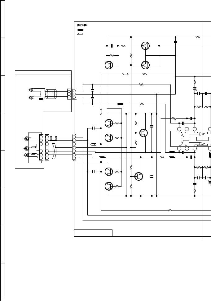
CD-DP2500W/DK2500W
A |
|
|
|
|
|
|
|
|
|
|
|
|
|
|
|
|
|
|
|
|
|
|
|
|
|
|
MIC SIGNAL |
|
|
|
|
|
|
|
|
|
|
|
|
|
|
|
|
|
|
|
|
PLAYBACK SIGNAL |
|
|
|
|
|
|
|
|
|
|
|
R174 |
|
|
|
|
|
|
|
|
RECORD SIGNAL |
|
|
|
|
|
|
|
|
|
|
|
|
|
|
|
|
|
|
|
|
|
|
|
|
|
|
|
|
|
|
|
|
150 |
|
|
|
|
|
|
|
|
|
C109 |
|
|
|
|
|
|
Q110 |
|
C153 |
|
|
|
|
|
|
|
|
|
|
|
0.047 |
|
|
|
2 |
|
KRC104 M |
|
100/16 |
|
|
|
||
|
|
|
|
|
|
|
|
R114 |
10K |
|
|
3 |
|
|
|
|
|
|
||
|
|
|
|
|
|
|
R113 |
|
|
|
1 |
|
|
|
|
|
|
|
||
|
|
|
|
|
|
|
|
|
|
|
|
|
|
|
|
|
|
|
|
|
|
|
|
|
|
|
|
10K |
|
|
R115 |
|
|
|
|
|
|
|
|
|
|
|
|
|
|
|
|
|
|
|
|
|
|
|
|
|
|
|
|
|
||
B |
|
|
|
|
|
|
|
|
|
4.7K |
|
1 |
|
|
|
|
|
|
|
|
|
|
|
|
|
|
|
|
|
|
|
|
|
|
|
|
|
|
|
||
|
|
|
|
|
|
|
|
|
|
|
|
|
|
|
|
|
|
|
|
|
|
|
|
|
|
|
|
|
|
|
|
2 |
|
3 |
|
|
|
|
|
|
|
|
|
|
|
|
|
|
Q109 |
|
|
|
|
|
Q111 |
|
|
|
|
|
|
|
TAPE MECHANISM ASS'Y(210) |
|
|
|
KTA1266 GR |
R112 |
|
KRC104 M |
|
|
|
|
|
||||||||
|
|
|
|
|
|
|
|
|
|
|
|
|
|
|
||||||
|
|
|
|
|
|
|
|
|
|
|
15K |
|
|
|
|
|
|
|
|
|
|
TAPE1 |
|
|
|
|
|
|
|
|
|
|
|
|
|
|
|
|
R120 |
|
|
|
|
|
|
|
|
|
|
|
|
|
R102 |
|
|
|
|
56 |
|
|
||
PLAYBACK HEAD |
|
|
|
|
|
|
|
|
|
|
|
|
|
C116 |
||||||
|
|
|
|
|
|
|
|
|
|
1K |
|
|
|
|
|
|||||
|
|
|
|
|
CNP101 C102 |
|
|
|
|
|
|
|
|
|
|
|
47/25 |
|||
R-CH |
|
|
TAPE1_R |
|
|
|
|
|
|
|
|
|
|
|
|
|
||||
|
|
|
3 |
3 |
0.001 |
|
|
|
|
|
|
|
|
|
|
|
|
|
|
|
|
|
|
A_GND |
|
|
|
|
|
|
|
|
|
|
|
|
|
|
|||
C |
|
|
2 |
|
|
|
|
|
|
|
|
|
|
|
|
|
|
|||
|
|
TAPE1_L |
2 |
C101 |
|
|
|
|
|
|
|
|
|
|
|
|
C118 |
C120 |
||
L-CH |
|
|
|
1 |
1 |
|
|
|
|
|
|
|
|
|
|
|
|
|||
|
|
|
|
|
0.001 |
|
|
|
|
|
|
|
|
|
|
|
|
0.033 |
560P |
|
|
|
|
CNS101 |
|
|
|
|
|
|
|
|
|
|
|
|
|
||||
|
|
|
|
|
|
|
|
|
|
|
R101 |
|
|
|
|
|
|
|
||
|
|
|
|
|
|
|
|
|
|
|
|
|
|
|
|
|
|
|
|
|
|
|
|
|
|
|
|
|
|
|
|
|
|
1K |
|
|
|
|
|
|
|
|
|
|
|
|
|
|
|
|
|
|
|
|
|
|
|
|
|
|
R122 |
|
|
|
|
|
|
|
|
|
|
|
|
|
|
|
|
|
R118 |
|
C114 |
100K |
|
|
|
|
|
|
|
|
Q104 |
|
|
R108 |
47K |
|
C108 |
0.001 |
|
1K |
C112 |
330P |
|
|
|
|
|
|
|
|
|
2SC1845 F |
|
|
|
|
|
|
|
|
|||||
|
|
|
|
|
|
C106 |
|
|
|
|
|
|
|
|
|
|
330P |
|
|
|
TAPE2 |
|
|
|
|
|
|
|
|
|
|
|
|
|
|
|
|
|
|
|
|
|
|
|
|
|
180P |
R104 |
|
|
|
|
|
|
|
|
|
|
|
|
|
|
RECORD/ |
|
|
|
|
|
|
|
|
|
|
|
|
|
|
|
24 |
23 |
22 |
2 |
|
PLAYBACK HEAD |
CNS102 |
|
|
|
|
2.2K |
|
|
|
|
|
|
|
|
|
|||||
D |
|
|
|
|
|
R106 |
|
|
|
|
|
|
|
|
|
|
|
- |
112K |
|
ERASE |
1 |
1 |
M_GND 1 |
|
3.3K |
|
|
R110 |
4.7K |
|
GR |
|
|
|
|
|
+ |
|
||
HEAD |
2 |
2 |
ERASE |
2 |
|
|
|
|
|
|
|
|
|
|
Hich=T1 |
|||||
|
|
|
|
|
|
|
|
|
|
|
|
|
||||||||
TAPE2_R1 |
|
|
|
|
|
|
Q108 KTC3199 |
|
|
|
1 |
2 |
3 |
4 |
||||||
|
3 |
3 |
TAPE2_R2 |
3 |
|
Q106 |
|
|
|
|
|
|
|
|
|
|
|
+ |
|
|
|
|
|
|
|
|
|
|
|
|
|
|
|
|
|
- |
112K |
||||
|
A_GND |
|
2SC1845 F |
|
|
|
|
|
|
|
|
|
|
|
|
|||||
R-CH |
|
|
|
|
4 |
|
|
|
|
|
|
|
|
|
|
|
|
|
|
|
|
4 |
4 |
TAPE2_L1 |
5 |
|
|
|
|
|
|
|
|
|
|
|
|
|
|
|
|
L-CH |
5 |
5 |
6 |
|
|
|
|
|
|
|
|
|
|
|
C111 |
|
|
|
||
TAPE2_L2 |
|
|
|
|
|
|
|
|
|
|
|
|
|
|
||||||
|
6 |
6 |
7 |
|
|
|
|
|
|
|
|
|
|
|
330P |
|
|
|
||
|
|
|
|
Q105 |
|
|
|
|
|
|
|
R117 |
C113 |
|
||||||
|
|
|
|
|
|
|
|
|
|
|
|
|
|
|
|
|||||
|
|
|
CNP102 |
|
|
|
|
|
|
KTC3199GR |
|
|
1K |
|
330P |
R121 R123 |
||||
|
|
|
|
2SC1845 F |
|
|
|
|
|
|
|
|
||||||||
|
|
|
|
|
|
C105 |
R105 |
|
|
R109 |
4.7K |
Q107 |
|
|
IC101 |
|
|
100K |
3.9K |
|
|
|
|
|
|
|
|
|
|
|
|
C117 |
|
560P |
|||||||
|
|
|
|
|
|
180P |
3.3K |
|
|
|
PLAYBACK AND |
|
||||||||
E |
|
|
|
|
|
|
|
|
|
|
|
|
|
|
|
AN7345K |
|
|
C119 |
|
|
|
|
|
|
|
|
R103 |
|
|
|
|
|
C107 |
0.001 |
|
RECORD/ |
0.033 |
|
|
|
|
|
|
|
|
|
|
|
|
|
|
|
PLAYBACK AMP. |
C115 |
|
47/25 |
|||||
|
|
|
|
|
|
|
2.2K |
|
|
|
|
|
|
|||||||
|
|
|
|
|
|
|
|
|
|
|
|
|
|
|
|
|
|
|
|
C121 |
|
|
|
|
|
|
|
|
|
R107 |
47K |
|
|
|
|
|
|
|
47/25 |
|
|
|
|
|
|
|
|
|
2SC1845 F |
|
|
|
|
|
|
|
|
56 |
|
|||
|
|
|
|
|
|
|
Q103 |
|
|
|
|
|
|
|
|
|
|
|
R119 |
|
F |
|
|
|
|
|
|
|
|
|
|
|
|
|
|
|
R111 |
|
|
|
|
|
|
|
|
|
|
|
|
|
|
|
|
|
|
|
|
15K |
|
|
|
|
MAIN PWB-A1(1/3)
G
H
• NOTES ON SCHEMATIC DIAGRAM can be found on page 16.
|
1 |
2 |
3 |
4 |
5 |
6 |
Figure 22 SCHEMATIC DIAGRAM (3/13)
– 22 –
 Loading...