


MANUAL
NTSC/PAL
CD-BK310V
SERVICE MANUAL
No. S6137CDBK310V
VIDEO CD MINI SYSTEM
MODEL CD-BK310V
CD-BK310V Video CD Mini System consisting of
CD-BK310V (main unit) and CP-BK310 (speaker system).
•In the interests of user-safety the set should be restored to its original condition and only parts identical to those specified be used.
CONTENTS |
|
|
Page |
SAFETY PRECAUTION FOR SERVICE MANUAL ........................................................................................................... |
2 |
VOLTAGE SELECTION ..................................................................................................................................................... |
2 |
AC POWER SUPPLY CORD AND AC PLUG ADAPTOR ................................................................................................. |
3 |
SPECIFICATIONS ............................................................................................................................................................. |
3 |
NAMES OF PARTS ........................................................................................................................................................... |
4 |
OPERATION MANUAL ...................................................................................................................................................... |
6 |
DISASSEMBLY .................................................................................................................................................................. |
9 |
REMOVING AND REINSTALLING THE MAIN PARTS ................................................................................................... |
12 |
ADJUSTMENT ................................................................................................................................................................. |
13 |
NOTES ON SCHEMATIC DIAGRAM .............................................................................................................................. |
18 |
TYPES OF TRANSISTOR AND LED ................................................................................................................................ |
18 |
BLOCK DIAGRAM ........................................................................................................................................................... |
19 |
SCHEMATIC DIAGRAM/WIRING SIDE OF P.W.BOARD ................................................................................................ |
24 |
VOLTAGE ........................................................................................................................................................................ |
43 |
WAVEFORMS OF CD CIRCUIT ...................................................................................................................................... |
44 |
TROUBLESHOOTING ..................................................................................................................................................... |
45 |
FUNCTION TABLE OF IC ................................................................................................................................................ |
49 |
FL DISPLAY ...................................................................................................................................................................... |
60 |
REPLACEMENT PARTS LIST/EXPLODED VIEW |
|
This document has been published to be used
SHARP CORPORATION– 1 – |
for after sales service only. |
|
|
|
The contents are subject to change without notice. |
CD-BK310V
SAFETY PRECAUTION FOR SERVICE MANUAL
WARNINGS
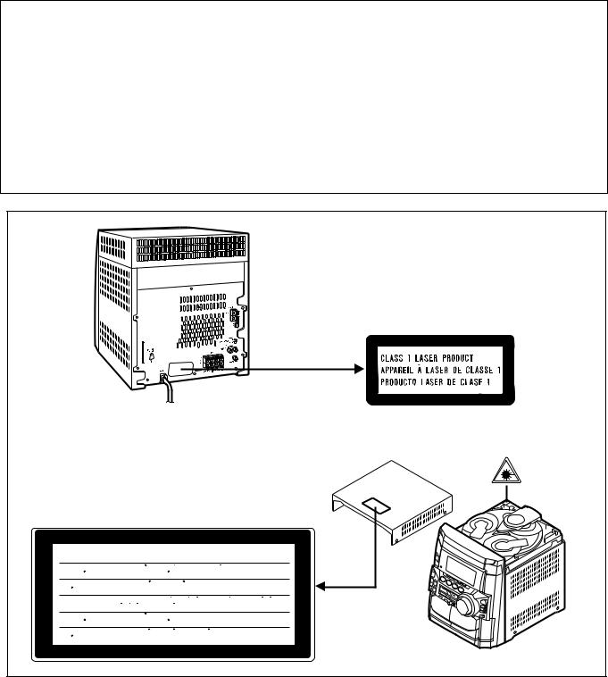
THE AEL (ACCESSIBLE EMISSION LEVEL) OF THE LASER POWER OUTPUT IS LESS THAN CLASS 1 BUT THE LASER COMPONENT IS CAPABLE OF EMITTING RADIATION EXCEEDING THE LIMIT FOR CLASS 1. THEREFORE IT IS IMPORTANT THAT THE FOLLOWING PRECAUTIONS ARE OBSERVED DURING SERVICING TO PROTECT YOUR EYES AGAINST EXPOSURE TO THE LASER BEAM.
1-WHEN THE CABINET IS REMOVED, THE POWER IS TURNED ON WITHOUT A COMPACT DISC IN POSITION AND THE PICKUP IS ON THE OUTER EDGE THE LASER WILL LIGHT FOR SEVERAL SECONDS TO DETECT A DISC. DO NOT LOOK INTO THE PICKUP LENS.
2-THE LASER POWER OUTPUT OF THE PICKUP UNIT AND REPLACEMENT SERVICE PARTS ARE ALL FACTORY PRESET BEFORE SHIPMENT.
DO NOT ATTEMPT TO READJUST THE LASER PICKUP UNIT DURING REPLACEMENT OR SERVICING. 3-UNDER NO CIRCUMSTANCES STARE INTO THE PICKUP LENS AT ANY TIME.
4-CAUTION-USE OF CONTROLS OR ADJUSTMENTS, OR PERFORMANCE OF PROCEDURES OTHER THAN THOSE SPECIFIED HEREIN MAY RESULT IN HAZARDOUS RADIATION EXPOSURE.
Laser Diode Properties
Material: GaAIAs
Wavelength: 780 nm
Emission Duration: continuous
Laser Output: max. 0.6 mW
CAUTION-INVISIBLE LASER RADIATION WHEN OPEN. DO NOT STARE INTO BEAM
OR VIEW DIRECTLY WITH OPTICAL INSTRUMENTS.
VARNING-OSYNLIG LASERSTRALNING NAR DENNA DEL AR OPPNAD. STIRRA EJ
IN I STRALEN OCH BETRAKTA EJ STRALEN MED OPTISKA INSTRUMENT.
ADVERSEL-USYNLIG LASERSTRALING VED ABNING. SE IKKE IND I
STRALEN-HELLER IKKE MED OPTISKE INSTRUMENTER.
VARO! AVATTAESSA OLET ALTTIINA NAKYMATON LASERSATEILYLLE. ALA
TUIJOTA SATEESEEN ALAKA KATSO SITA OPTISEN LAITTEEN LAPI.
VARNING-OSYNLIG LASERSTRALNING NAR DENNA DEL AR OPPNAD. STIRRA EJ
IN I STRALEN OCH BETRAKTA EJ STRALEN GENOM OPTISKT INSTRUMENT.
ADVERSEL-USYNLIG LASERSTRALING NAR DEKSEL APNES. STIRR IKKE INN I
STRALEN ELLER SE DIREKTE MED OPTISKE INSTRUMENTER.
VOLTAGE SELECTION
Before operating the unit on mains, check the preset voltage. If the voltage is different from your local voltage, adjust the voltage as follows.
Turn the selector with a screwdriver until the appropriate voltage number appears in the window (110 V, 127 V, 220 V or 230 V-240 V AC).
– 2 –
CD-BK310V
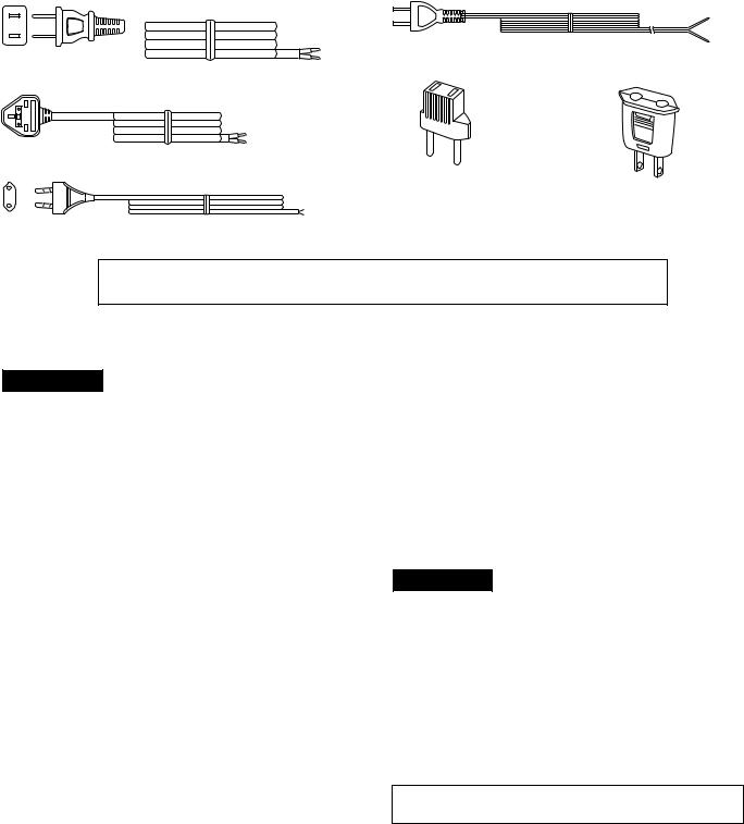
AC POWER SUPPLY CORD AND AC PLUG ADAPTOR
QACCA0003AW00 |
|
QACCJ0007AW00 |
||
|
|
|
|
|
|
|
|
|
|
|
|
|
|
|
|
|
|
|
|
|
|
|
|
|
|
|
|
|
|
QPLGA0003AWZZ QPLGA0004AWZZ
QACCB0011AW00
QACCE0010AW00
FOR A COMPLETE DESCRIPTION OF THE OPERATION OF THIS UNIT, PLEASE REFER TO THE OPERATION MANUAL.
SPECIFICATIONS
CD-BK310V
 General
Power source |
AC 110/127/220/230 - 240 V, 50/60 Hz |
|
|
Power consumption |
210 W |
Dimensions |
Width: 270 mm (10-11/16") |
|
Height: 330 mm (13") |
|
Depth: 372 mm (14-11/16") |
Weight |
8.7 kg (19.2 lbs.) |
|
|
 Amplifier
Output power |
MPO: 480 W (240 W + 240 W) (10 % T.H.D.) |
|
Main speaker (woofer and tweeter): 200 W (100 W + 100 |
|
W) |
|
Subwoofer: 280 W (140 W + 140 W) |
|
RMS: 250 W (125 W + 125 W) (10 % T.H.D.) |
|
Main speaker (woofer and tweeter): 100 W (50 W + 50 W) |
|
Subwoofer: 150 W (75 W + 75 W) |
|
RMS: 188 W (94 W + 94 W) (0.9 % T.H.D.) |
|
Main speaker (woofer and tweeter): 72 W (36 W + 36 W) |
|
Subwoofer: 116 W (58 W + 58 W) |
|
|
Output terminals |
Speakers: 6 ohms |
|
Headphones: 16 - 50 ohms (recommended: 32 ohms) |
Input terminals |
Video/Auxiliary (audio signal): 500 mV/47 kohms |
|
Microphone: 1 mV/600 ohms |
|
|
 Video CD
Video output format |
PAL/NTSC |
 CD player
Type |
3-disc multi-play compact disc player |
|
|
Signal readout |
Non-contact, 3-beam semiconductor laser pickup |
|
|
D/A converter |
1-bit D/A converter |
|
|
Frequency response |
20 - 20,000 Hz |
|
|
Dynamic range |
90 dB (1 kHz) |
|
|
 Tuner
Tuner
Frequency range |
FM: 88 - 108 MHz |
|
AM: 531 - 1,602 kHz |
 Cassette deck
Frequency response |
50 - 14,000 Hz (Normal tape) |
Signal/noise ratio |
55 dB (TAPE 1, playback) |
|
50 dB (TAPE 2, recording/playback) |
|
|
Wow and flutter |
0.3 % (WRMS) |
CP-BK310
Type |
3-way type speaker system |
|
5 cm (2") Tweeter |
|
13 cm (5-1/4") Woofer |
|
16 cm (6-1/2") Subwoofer |
|
|
Maximum input power |
250 W |
(Total) |
|
|
|
Rated input power |
125 W |
(Total) |
|
Impedance |
6 ohms |
|
|
Dimensions |
Width: 287 mm (11-5/16") |
|
Height: 330 mm (13") |
|
Depth: 281 mm (11-1/16") |
|
|
Weight |
5.0 kg (11.1 lbs.)/each |
|
|
Specifications for this model are subject to change without prior notice.
– 3 –
CD-BK310V
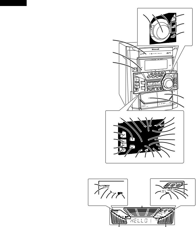
NAMES OF PARTS
CD-BK310V
 Front panel
1.Video CD/CD/MP3 Disc Tray
2.Timer Set Indicator
3.On/Stand-by Button
4.Tape 2 Cassette Compartment
5.Tape 1 Cassette Compartment
6.Equalizer Mode Select Button
7.Volume Control
8.Extra Bass/Demo Mode Button
9.Video CD/CD/MP3 Disc Tray Open/Close Button 10.Video CD/CD/MP3 Disc Number Select Buttons
(with Indicator)
11.Video CD/CD/MP3 Disc Skip Button 12.Tape 2 Reverse Play Button (with Indicator) 13.Video CD/CD/MP3 Disc Button
14.Karaoke Mode Button 15.Tuner (Band) Button
16.Video CD Playback Control Button 17.Video CD On Screen Display On/Off Button 18.Video CD Digest Button
19.Tuning and Time Up Button 20.Dimmer Button
21.Clock Button 22.Timer/Sleep Button 23.Headphone Socket 24.Video/Auxiliary Button 25.Tape (1  2) Button
26.Video CD Stop or Return, CD/MP3 Disc/Tape Stop Button (with Indicator)
27.Video CD Play or Repeat or Select or Resume, CD/MP3 Disc Play or Repeat, Tape 1 Play, Tape 2 Forward Play Button
(with Indicator)
28.Tape 2 Reverse Mode Select Button
29.Video CD Skip or Next, CD/MP3 Disc Track Up or Fast Forward, Tape 2 Fast Wind, Tuner Preset Up Button
30.Tuning and Time Down Button 31.Memory/Set Button
32.Tape 2 Record Pause Button
33.Video CD Skip or Previous, CD/MP3 Disc Track Down or Fast Reverse, Tape 2 Fast Wind, Tuner Preset Down Button
34.Microphone Level Control 35.Microphone Socket
6 |
7 |
8 |
9 |
|
|
|

 10
10  11
11
1
2
3
4
5
12 |
13 |
14 |
15 |
16 |
17 |
18 |
|||||
19 |
|
|
|
|
|
|
|
|
|
|
24 |
|
|
|
|
|
|
|
|
|
|
25 |
|
20 |
|
|
|
|
|
|
|
|
|
|
|
|
|
|
|
|
|
|
|
|
|
26 |
|
21 |
|
|
|
|
|
|
|
|
|
|
27 |
22 |
|
|
|
|
|
|
|
|
|
|
28 |
|
|
|
|
|
|
|
|
|
|
29 |
|
23 |
|
|
|
|
|
|
|
|
|
|
|
|
|
|
|
|
|
|
|
|
|
|
|
30 |
31 |
32 |
33 |
34 |
35 |
||||||
 Display
1.Extra Bass Indicator
2.FM Stereo Mode Indicator
3.FM Stereo Receiving Indicator
4.Karaoke Mode Indicator
5.Video CD/CD/MP3 Disc Repeat Play Indicator
6.Video CD/CD/MP3 Disc Pause Indicator
7.Video CD/CD/MP3 Disc Play Indicator
8.Tape 2 Record Indicator
9.Tape Reverse Mode Indicator
10.Video CD/CD/MP3 Disc Number Indicators 11.Timer Play Indicator
12.Memory Indicator
13.Tape 2 Reverse Play Indicator
14.Tape 1 Play or Tape 2 Forward Play Indicator 15.Sleep Indicator
16.Timer Recording Indicator
17.Spectrum Analyser/Volume Level Indicator
1 |
|
8 |
|
10 |
|
|
|
11 |
|
2 |
|
9 |
|
|
|
|
12 |
||
3 4 5 6 |
7 |
17 |
13 |
14 15 16 |
17 |
17 |
– 4 –
CD-BK310V
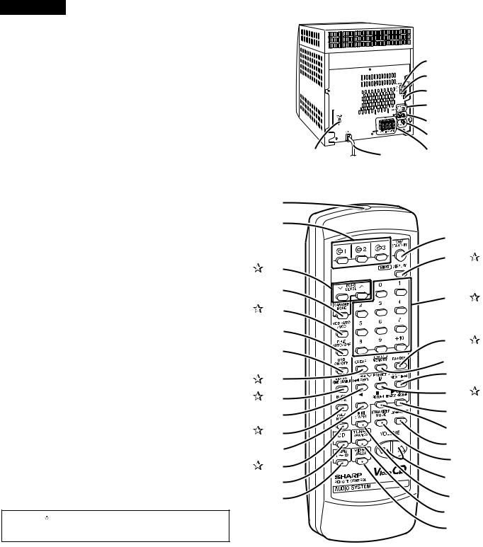
 Rear panel
1.FM 75 Ohms Aerial Terminal
2.FM Aerial Earth Terminal
3.AM Loop Aerial Socket
4.Span Selector Switch
5.Video/Auxiliary (Audio Signal) Input Sockets
6.Video Output Socket
7.Speaker Terminals
8.AC Power Lead
9.AC Voltage Selector
 Remote control
1.Remote Control Transmitter
2.Video CD/CD/MP3 Disc Number Select Buttons
3.Echo Level Up and Down Buttons
4.Karaoke Mode Button
5.Video CD Auto/On Button
6.Video CD Playback Control Auto/Off Button
7.Video CD On Screen Display On/Off Button
8.Video CD/CD/MP3 Disc Clear Button
9.Video CD Digest/Time Search Button
10.Video CD Skip or Previous, CD/MP3 Disc Track Down or Fast Reverse, Tape 2 Fast Wind, Tuner Preset Down Button
11.Video CD Bookmark Button 12.Tape 2 Reverse Play Button
13.PAL/NTSC Select Button 14.Video CD/CD/MP3 Disc Button 15.Tape (1 2) Button 16.On/Stand-by Button
17.MP3 Disc Display Button
18.Video CD/CD/MP3 Disc Direct Search Buttons 19.Video CD/CD/MP3 Disc Random Button 20.Video CD/CD/MP3 Disc Memory Button
21.Video CD Skip or Next, CD/MP3 Disc Track Up or Fast Forward, Tape 2 Fast Wind, Tuner Preset Up Button
22.Video CD/CD/MP3 Disc Pause Button
23.Video CD Play or Repeat or Select or Resume, CD/MP3 Disc Play or Repeat, Tape 1 Play, Tape 2 Forward Play Button
24.Video CD Stop or Return, CD/MP3 Disc/Tape Stop Button 25.Extra Bass Button
26.Equalizer Mode Select Button
27.Volume Up and Down Buttons
28.Tape 2 Record Pause Button
29.Tuner (Band) Button
30.Video/Auxiliary Button
Buttons with " " mark in the illustration can be operated on the remote control only.
Other buttons can be operated both on the main unit and the remote control.
CD-BK310V
|
|
1 |
|
|
2 |
|
|
3 |
|
|
4 |
|
|
5 |
|
|
6 |
9 |
8 |
7 |
1 |
|
|
2 |
16 |
|
|
||
3 |
17 |
|
|
||
4 |
18 |
|
5 |
||
|
||
6 |
19 |
|
7 |
||
20 |
||
|
||
8 |
21 |
|
9 |
22 |
|
23 |
||
10 |
||
24 |
||
11 |
||
12 |
25 |
|
26 |
||
13 |
||
27 |
||
14 |
||
15 |
28 |
|
|
29 |
|
|
30 |
– 5 –
CD-BK310V
CP-BK310
 Speaker system
1.Subwoofer
2.Bass Reflex Duct
3.Tweeter
4.Woofer
5.Speaker wire for SUBWOOFER terminals
6.Speaker wire for MAIN terminal
 3
3
1
2 |
4 |
5 |
|
|
|
|
|
6 |
OPERATION MANUAL
|
Setting the AC voltage selector |
|
Setting the FM/AM span selector |
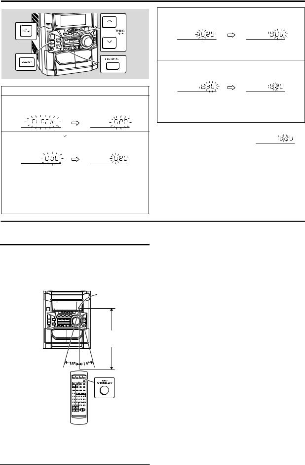
Check the setting of the AC voltage selector located on the rear panel before plugging the unit into a wall socket. If necessary, adjust the selector to correspond to the AC power voltage used in your area.
Turn the selector with a screwdriver until the appropriate voltage number appears in the window (110 V, 127 V, 220 V or 230 V - 240 V AC).
 Connecting the AC power lead
After making all connections, plug the unit. If you plug the unit first, the unit will enter the demonstration mode.
Note:
Unplug the AC power lead from the wall socket if the unit will not be in use for a prolonged period of time.
AC Plug Adaptor
In areas (or countries) where a wall socket as shown in illustration  is used, connect the unit using the AC plug adaptor supplied with the unit, as illustrated. The AC plug adaptor is not included in areas where the wall socket and AC power plug can be directly connected (see illustration
  ).
).
 1
1
 2
2
The International Telecommunication Union (ITU) has established that member countries should maintain either a 100 kHz or a 50 kHz interval between broadcasting frequencies of FM stations and 10 kHz or 9 kHz for AM station. The illustration shows the 50/9 kHz zones (regions 1 and 3), and the 100/10 kHz zone (region 2).
Before using the unit, set the SPAN SELECTOR switch (on the rear panel) to the interval (span) of your area.
To change the tuning zone:
1Press the ON/STAND-BY button to enter the stand-by mode.
2Set the SPAN SELECTOR switch (on the rear panel) as follows.
 For 50 kHz FM interval (9 kHz in AM)
  50/9
50/9
 For 100 kHz FM interval (10 kHz in AM)
  100/10
3Whilst pressing down the  button and the X-BASS/DEMO button, press the ON/ STAND-BY button until "CLEAR AL" appears.
Caution:
This operation will erase all data stored in memory including clock, timer settings, tuner preset, and CD programme.
– 6 –
CD-BK310V
Setting the Clock
In this example, the clock is set for the 24-hour (0:00) display.
1 Press the ON/STAND-BY button to turn the power on.
2 Press the CLOCK button and within 5 seconds, press the MEMORY/SET button.
3 Press the TUNING/TIME ( or  ) button to select 24-hour or 12hour display and then press the MEMORY/SET button.
"0:00"  The 24-hour display will appear. (0:00 - 23:59)
"AM 12:00"  The 12-hour display will appear. (AM 12:00 - PM 11:59)
"AM 0:00"  The 12-hour display will appear. (AM 0:00 - PM 11:59)
Note that this can only be set when the unit is first installed or it has been reset.
4 Press the TUNING/TIME ( or ) button to adjust the hour and then press the MEMORY/SET button.
 Press the TUNING/TIME (
 or
or  ) button once to advance the time by 1 hour. Hold it down to advance continuously.
 When the 12-hour display is selected, "AM" will change automatically to "PM".
5 Press the TUNING/TIME ( or
or  ) button to adjust the minutes and then press the MEMORY/SET button.
 Press the TUNING/TIME (
 or
or  ) button once to advance the time by 1 minute. Hold it down to change the time in 5-minute intervals.
 The hour will not advance even if minutes advance from "59" to "00".
 The clock begins counting from "0" seconds. (Seconds are not displayed.) The time display will disappear after a few seconds.
To confirm the time display:
Press the CLOCK button.
The time display will appear for about 5 seconds.
Note:
The "CLOCK" or time will flash at the push of the CLOCK button when the AC power supply is restored after a power failure or unplugging the unit.
Readjust the clock as follows.
To readjust the clock:
Perform "Setting the Clock" from the beginning. If the time display is flashing, step 3 (for selecting the 24-hour or 12-hour display) will be skipped.
To change the 24-hour or 12-hour display:
1Clear all the programmed contents.
2Perform "Setting the Clock" from the beginning.
Remote Control
 Test of the remote control
Face the remote control directly to the remote sensor on the unit.
The remote control can be used within the range shown below:
Press the ON/STAND-BY button. Does the power turn on? Now, you can enjoy the music.
Remote sensor
0.2 m - 6 m (8" - 20')
– 7 –
CD-BK310V
Troubleshooting Chart
Many potential problems can be resolved by the owner without calling a service technician.
If something is wrong with this product, check the following before calling your authorised SHARP dealer or service centre.
 General
|
|
Symptom |
Possible cause |
|
|
The clock is not on time. |
Did a power failure occur? Reset the |
|
|
|
clock. |
|
|
|
|
|
|
When a button is pressed, the unit |
Set this unit to the power stand-by mode |
|
|
does not respond. |
and then turn it back on. |
|
|
|
If the unit still malfunctions, reset it. |
|
|
|
|
|
|
No sound is heard. |
Is the volume level set to "0"? |
|
|
|
Are the headphones connected? |
|
|
|
Are the speaker wires disconnected? |
|
|
|
Is the karaoke mode set to "L-CH", "R-CH" |
|
|
|
or "V-CANCEL"? |
|
|
Video CD |
|
|
|
|
|
|
|
|
|
|
|
|
|
|
|
Symptom |
Possible cause |
|
|
The picture is not displayed during |
Is the TV unplugged? |
|
|
playback. |
Is the unit connected improperly? |
|
|
|
Is the input selector on the TV set to other |
|
|
|
than "VCR"? |
|
|
|
Is the unit being played without selecting |
|
|
|
video CD? |
|
|
The picture quality is poor, or it is |
Is the disc very dirty? |
|
|
distorted. |
|
 Tuner
Tuner
Symptom |
Possible cause |
Radio makes unusual noise con- |
Is the unit placed near the TV or comput- |
secutively. |
er? |
|
Is the FM aerial or AM loop aerial placed |
|
properly? Move the AC power lead away |
|
from the aerial if located near. |
 Cassette deck
Symptom |
Possible cause |
Cannot record. |
Is the erase-prevention tab removed? |
Cannot record tracks with proper |
Is it a normal tape? (You cannot record on |
sound quality. |
a metal or CrO tape.) |
Cannot erase completely. |
|
Sound skipping. |
Is there any slack? |
|
Is the tape stretched? |
Cannot hear treble. |
Are the capstans, pinch rollers, or heads |
Sound fluctuation. |
dirty? |
Cannot remove the tape. |
If a power failure occurs during playback, |
|
the heads remain engaged with the tape. |
|
Do not open the compartment forcibly. |
|
Wait until electricity resumes. |
 Karaoke
Symptom |
Possible cause |
The vocal part of a multiplexed |
Is the karaoke mode set to "L-CH", "R-CH" |
disc is not heard. |
or "V-CANCEL"? |
 CD player
Symptom |
Possible cause |
Playback does not start. |
Is the disc loaded upside down? |
Playback stops in the middle or is |
Does the disc satisfy the standards? |
not performed properly. |
Is the disc distorted or scratched? |
Playback sounds are skipped, or |
Is the unit located near excessive vibra- |
stopped in the middle of a track. |
tions? |
|
Is the disc very dirty? |
|
Has condensation formed inside the unit? |
|
|
 Remote control
Symptom |
Possible cause |
The remote control does not oper- |
Is the AC power lead of the unit plugged |
ate. |
in? |
|
Is the battery polarity respected? |
|
Are the batteries dead? |
|
Is the distance or angle incorrect? |
|
Does the remote control sensor receive |
|
strong light ? |
Troubleshooting Chart
 If trouble occurs
When this product is subjected to strong external interference (mechanical shock, excessive static electricity, abnormal supply voltage due to lightning, etc.) or if it is operated incorrectly, it may malfunction.
If such a problem occurs, do the following:
1Set the unit to the stand-by mode and turn the power on again.
2If the unit is not restored in the previous operation, unplug and plug in the unit, and then turn the power on.
Note:
If neither operation above restores the unit, clear all the memory by resetting it.
 Clearing all the memory (reset)
1Press the ON/STAND-BY button to enter the power stand-by mode.
2Whilst pressing down the  button and the X-BASS/DEMO button, press the ON/ STAND-BY button until "CLEAR AL" appears.
Caution:
This operation will erase all data stored in memory including clock, timer settings, tuner preset, and CD programme.
 Before transporting the unit
1Press the ON/STAND-BY button to turn the power on.
2Press the CD/VIDEO CD button.
3Press the OPEN/CLOSE button to open the disc tray.
Remove all discs from the unit.
4Press the OPEN/CLOSE button to close the disc tray.
Make sure that "NO DISC" is displayed.
5Press the ON/STAND-BY button to enter the stand-by mode, and then unplug the AC power lead from the wall socket.
– 8 –
CD-BK310V
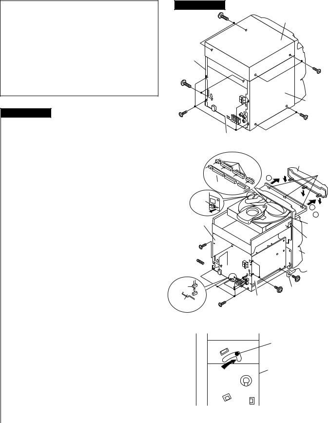
DISASSEMBLY
Caution on Disassembly
Follow the below-mentioned notes when disassembling the unit and reassembling it, to keep it safe and ensure excellent performance:
1.Take cassette tape and compact disc out of the unit.
2.Be sure to remove the power supply plug from the wall outlet before starting to disassemble the unit.
3.Take off nylon bands or wire holders where they need to be removed when disassembling the unit. After servicing the unit, be sure to rearrange the leads where they were before disassembling.
4.Take sufficient care on static electricity of integrated circuits and other circuits when servicing.
CD-BK310V
STEP |
REMOVAL |
|
PROCEDURE |
|
|
FIGURE |
|
|
|
|
|
|
|
|
|
1 |
Top Cabinet |
1. |
Screw ....................... |
(A1) x4 |
9-1 |
||
|
|
|
|
|
|
|
|
2 |
Side Panel |
1. |
Screw ....................... |
(B1) x8 |
9-1 |
||
|
(Left/Right) |
|
|
|
|
|
|
|
|
|
|
|
|
|
|
3 |
CD Player Unit/ |
1. |
Turn on the power supply, |
... |
9-2 |
||
|
CD Tray Cover |
|
open the disc tray, take out |
|
|
||
|
|
|
|
the CD tray cover, and close. |
|
||
|
|
|
|
(Note 1) |
|
|
|
|
|
|
2. |
Screw ....................... |
(C1) x1 |
|
|
|
|
|
3. |
Hook ......................... |
(C2) x3 |
|
|
|
|
|
4. |
Hook ......................... |
(C3) x2 |
|
|
|
|
|
5. |
Socket ...................... |
(C4) x4 |
|
|
|
|
|
|
|
|
|
|
4 |
Rear Panel with |
1. |
Screw ..................... |
(D1) x10 |
9-2 |
||
|
Fan Motor |
2. |
Socket ...................... |
(D2) x1 |
|
||
5 |
Main PWB |
1. |
Screw ....................... |
(E1) x1 |
9-2 |
||
|
|
|
2. |
Flat Cable ................ |
(E2) x1 |
10-2 |
|
|
|
|
3. |
Socket ...................... |
(E3) x5 |
10-2,10-3 |
|
6 |
Amp. PWB |
1. |
Screw ....................... |
(F1) x5 |
10-3 |
||
|
|
|
2. |
Socket ...................... |
(F2) x2 |
|
|
|
|
|
3. |
PWB Holder ............. |
(F3) x2 |
|
|
|
|
|
4. |
Flat Wire ................... |
(F4) x1 |
|
|
|
|
|
|
|
|
|
|
7 |
Front Panel |
1. |
Screw ....................... |
(G1) x1 |
10-3 |
||
|
|
|
|
|
|
|
|
8 |
Display PWB |
1. Knob ......................... |
(H1) x1 |
10-4 |
|||
|
|
|
2. |
Screw ..................... |
(H2) x12 |
|
|
|
|
|
3. |
Flat Cable ................ |
(H3) x1 |
|
|
9 |
Tape Mechanism |
1. |
Open the cassette holder. |
10-4 |
|||
|
|
|
2. |
Screw ........................ |
(J1) x5 |
|
|
|
|
|
|
|
|
|
|
10 |
Headphones PWB |
1. |
Screw ....................... |
(K1) x1 |
10-4 |
||
|
|
|
|
|
|
|
|
11 |
Mic PWB |
1. |
Screw ....................... |
(L1) x2 |
10-4 |
||
|
|
|
|
|
|
|
|
12 |
Turntable |
1. |
Hook ........................ |
(M1) x2 |
10-5 |
||
|
|
|
2. |
Cover ...................... |
(M2) x1 |
|
|
|
|
|
|
|
|
|
|
13 |
Disc Tray |
1. |
Turn fully the lock lever in the . |
9-3 |
|||
|
|
|
|
arrow direction. |
|
|
|
|
|
|
2. |
While holding the lock lever, rotate |
10-1 |
||
|
|
|
|
the cam gear until the cam gear |
|
||
|
|
|
|
rib engages with the clamp lever. |
|
||
|
|
|
3. |
Push the slide chassis backward to |
10-6 |
||
|
|
|
|
engage the claw with the groove |
|
||
|
|
|
|
and remove it in the direction |
|
||
|
|
|
|
of the arrow. ................. |
(N1) x6 |
|
|
|
|
|
|
|
|
|
|
14 |
Video CD PWB |
1. |
Screw ....................... |
(P1) x1 |
11-1 |
||
|
(Note 2) |
2. |
Hook ......................... |
(P2) x2 |
|
||
|
|
|
3. |
Socket ...................... |
(P3) x4 |
|
|
|
|
|
|
|
|
|
|
15 |
CD Mechanism |
1. Hook ......................... |
(Q1) x2 |
11-2 |
|||
|
|
|
2. |
Hook ......................... |
(Q2) x3 |
|
|
|
|
|
|
|
|
|
|
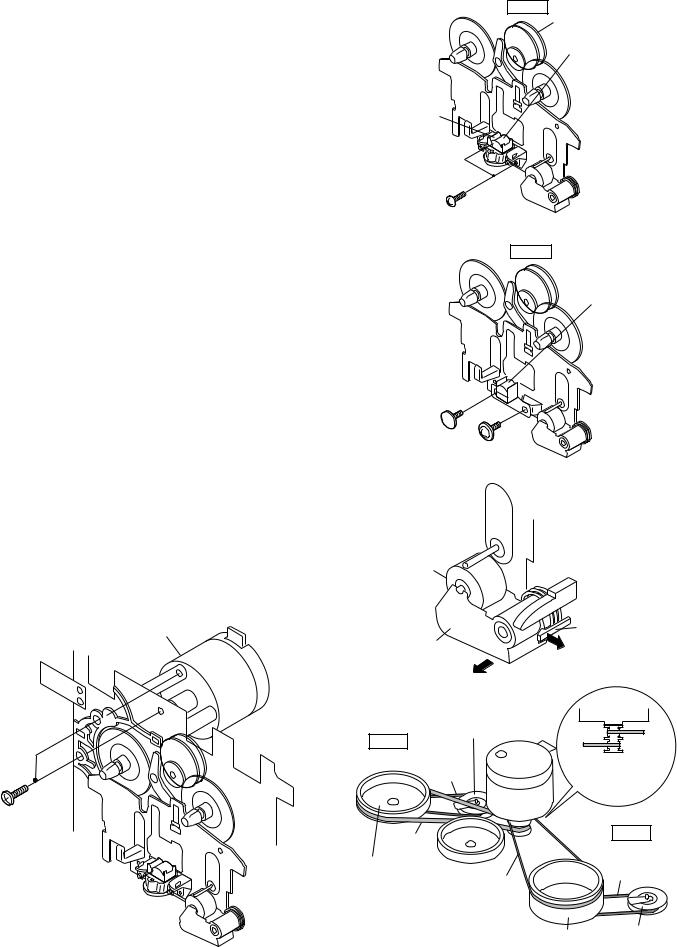
Note 1: How to open the changer manually. (Fig. 9-3)
1.In this state, turn fully the lock lever in the arrow direction through the hole on the loading chassis bottom.
2.While holding the lock lever, rotate the cam gear anticlockwise until the cam gear rib engages with the clamp lever. (Fig. 10-1)
3.After that, push forward the slide Chassis.
CD-BK310V
(A1) x 2
Top Cabinet
ø3 x 12mm
Side Panel (Right)
(B1) x 2 ø3 x 10mm
(B1) x 4 ø3 x 10mm
Rear
Panel Figure 9-1
(C4) x 4
1
Video
CD PWB
(C3) x 1
Pull
Rear
Panel
(C1) x 1 ø3 x 10mm
(D1) x 1
ø3 x 10mm 
Transformer PWB 
(D2) x 1 |
|
Amp. |
Main PWB |
|
|
PWB |
(D1) x 7 |
|
|
|
ø3 x 10mm |
(A1) x 2 ø3 x 12mm
Side Panel (Left)
(B1) x 2 ø3 x 10mm
CD Tray Cover
(C2) x 3
1
 2
2
CD Player
Unit
(C3) x 1
Front Panel
(E1) x 1 ø3 x 10mm
Lug Wire
(D1) x 2 ø3 x 10mm
Figure 9-2
Lock Lever
CD Player Unit
(Bottom View)
Figure9-3
Note 2:
1. After removing the connector for the optical pickup from the connector, wrap the conductive aluminium foil around the front end of the connector so as to protect the optical pickup from electrostatic damage.
Note 3:
1.Be careful not to break the claw of the CD mechanism.
2.When fining back the cam gear assembly, let it lock by front movement.
– 9 –

CD-BK310V
Clamp Lever
CD Player Unit
(Top View)
Cam Gear Rib
|
(H1) x 1 |
|
Display PWB |
(H3) x 1 |
|
|
||
|
(L1) x 2 |
|
(H2) x 12 |
ø3 x 10mm |
|
|
||
ø3 x 10mm |
|
|
|
Mic PWB |
|
Tape |
|
|
Mechanism |
Front Panel |
|
Lug Wire |
||
|
||
(J1) x 5 |
Open |
|
ø3 x 10mm |
|
|
|
Cassette |
|
|
Holder |
|
Figure 10-1 |
(K1) x 1 |
|
|
ø3 x 10mm |
|
(E3) x 1 |
Headphones |
|
(E3) x 1 |
|
|
PWB |
|
|
Front Panel |
Figure 10-4 |
Power PWB |
|
|
(E2) x 1 |
(E3) x 1 |
(M2) x 1 |
|
|
|
|
Mic PWB |
|
Transformer |
|
Turntable |
|
|
|
PWB |
Main PWB |
|
|
|
|
|
Main PWB |
|
|
(E3) x 1 |
Slide |
|
Chassis |
|
|
|
|
|
|
(M1) x 2 |
|
Amp. |
|
|
PWB |
|
|
Figure 10-2 |
|
|
|
|
(F1) x 2 |
|
|
|
|
ø3 x 6mm |
(F4) x 1 |
|
|
|
|
|
||
|
(F1) x 2 |
|
|
CD Player Unit |
|
ø3 x 6mm |
Headphones |
||
|
|
|
||
|
|
PWB |
|
Figure 10-5 |
|
|
|
|
|
|
(F2) x 2 |
|
Front |
(N1) x 3 |
|
Tape |
|
Panel |
3 |
|
Mechanism |
|
|
|
|
|
|
|
|
(E3) x 1 |
|
|
|
|
|
|
|
|
2 |
(F3) x 1 |
|
|
1 |
|
|
|
|
||
Push |
Push |
(F3) x 1 |
|
|
|
|
Push |
Push |
(N1) x 3 |
|
(F1) x 1 |
|
|
|
|
|
|
|
|
|
ø3 x 6mm |
(G1) x 1 |
|
|
|
Amp. |
|
|
|
|
ø3 x 10mm |
|
|
|
|
PWB |
|
|
|
|
|
|
|
|
|
Figure 10-3 |
|
|
Figure 10-6 |
– 10 –
|
|
|
CD-BK310V |
|
|
CD |
(Q2) x 3 |
|
|
Mechanism |
|
(P1) x 1 |
Video CD |
Slide |
|
ø3 x 8mm |
|
||
Chassis |
|
||
|
PWB |
CD |
|
|
|
||
(P3) x 2 |
|
|
|
|
|
Mechanism |
|
|
|
|
|
(P2) x 2 |
|
(Q1) x 1 |
(Q1) x 1 Chassis |
|
|
|
(P3) x 2
Slide
Chassis
Figure 11-1
Figure 11-2
CP-BK310
STEP |
REMOVAL |
PROCEDURE |
|
FIGURE |
|
|
1 |
Side Panel/ |
1. Screw ..................... |
(A1) x4 |
11-3 |
|
|
|
Front Panel |
2. Hook ....................... |
(A2) x3 |
|
|
|
|
|
3. Net .......................... |
(A3) x1 |
|
|
|
|
|
4. Caching Holder ...... |
(A4) x4 |
|
|
|
|
|
5. Screw ..................... |
(A5) x4 |
|
|
|
2 |
Subwoofer |
1. Screw ..................... |
(B1) x4 |
11-4 |
|
|
3 |
Woofer |
1. Screw ..................... |
(C1) x4 |
11-4 |
|
|
4 |
Tweeter |
1. Screw ..................... |
(D1) x2 |
11-4 |
|
(C1) x 4 |
|
|
|
|
|
|
ø4 x 16mm |
|
|
|
|
|
|
(D1) x 2 |
|
|
|
|
|
|
ø3 x 10mm |
|
(A4) x 2 |
|
(A3) x 1 |
|
|
|
|
|
|
|
|
|
|
|
|
|
|
(A4) x 2 |
Woofer |
Tweeter |
|
|
|
|
|
||
|
(A5) x 2 |
|
|
|
|
|
|
ø4 x 20mm |
|
(A5) x 2 |
|
|
|
|
|
|
|
|
||
|
|
|
ø4 x 20mm |
|
|
|
|
Side Panel |
|
|
|
|
|
|
|
|
Fromt Panel |
|
|
|
(A1) x 4 |
(B1) x 4 |
ø4 x 20mm |
|
|
ø4 x 16mm |
Subwoofer
(A2) x 3
Figure 11-4
Figure 11-3
– 11 –
CD-BK310V
REMOVING AND REINSTALLING THE MAIN PARTS
TAPE MECHANISM SECTION
Perform steps 1 to 7 and 9 of the disassembly method to remove the tape mechanism.
How to remove the record/playback and erase heads (TAPE 2) (See Fig. 12-1)
1.When you remove the screws (A1) x 2 pcs., the recording/ playback head and three-dimensional head of the erasing head can be removed.
How to remove the playback head (TAPE 1) (See Fig. 12-2)
1.When you remove the screws (B1) x 2 pcs., the playback head.
How to remove the pinch roller (TAPE 1/2) (See Fig. 12-3)
1. Carefully bend the pinch roller pawl in the direction of the arrow <A>, and remove the pinch roller (C1) x 1 pc., in the direction of the arrow <B>.
Note:
When installing the pinch roller, pay attention to the spring mounting position.
How to remove the belt (TAPE 2) (See Fig. 12-4)
1.Remove the main belt (D1) x 1 pc., from the motor side.
2.Remove the FF/REW belt (D2) x 1 pc.
How to remove the belt (TAPE 1) (See Fig. 12-4)
1.Remove the main belt (E1) x 1 pc., from the motor side.
2.Remove the FF/REW belt (E2) x 1 pc.
How to remove the motor (See Fig. 12-5)
1. Remove the screws (F1) x 2 pcs., to remove the motor.
Tape
Motor
 Clutch Ass'y
(F1) x 2
Ø2.6 x 5mm
TAPE 2
Clutch Ass'y
Record/Playback
Head
Erase Head
(A1) x 2 Ø2 x 6mm
Figure 12-1
TAPE 1
 Clutch Ass'y
Playback
Head
(B1) x 1  Ø2 x 9mm
(B1) x 1 Ø2 x 5mm
Figure 12-2
|
|
Pinch |
|
|
|
Roller |
|
Pinch Roller |
|
Pawl |
|
(C1) x 1 |
Pull |
Pull <A> |
|
|
|
||
|
<B> |
|
|
|
Figure 12-3 |
|
|
|
|
Tape |
|
|
FF/REW |
Motor |
|
|
Tape |
|
|
TAPE 2 |
Roller |
Motor |
TAPE 1 |
|
|
||
FF/REW |
TAPE 2 |
Main Belt |
|
Belt |
|
(E1) x 1 |
|
|
Main Belt |
||
(D2) x 1 |
|
||
(D1) x 1 |
|
||
|
|
|
|
Main Belt |
|
|
TAPE 1 |
|
|
|
|
(D1) x 1 |
|
|
FF/REW |
Flywheel |
|
|
|
|
|
Belt |
|
Ass'y |
Main Belt |
(E2) x 1 |
|
|
|
||
|
(E1) x 1 |
|
|
|
|
Flywheel |
FF/REW |
|
|
Ass'y |
Roller |
Figure 12-5 |
Figure 12-4 |
– 12 –

CD MECHANISM SECTION
Perform steps 1, 2, 3, 12, 13, 14 and 15 of the disassembly method to remove the CD mechanism.
How to remove the CD loading motor (See Fig. 13-1)
1.Bend the hooks (A1) x 5 pcs., to remove the CD loading motor.
2.Remove the drive belt (A2) x 1pc.
|
CD-BK310V |
|
CD Loading Motor |
Slide |
CD Loading |
Chassis |
Motor PWB |
|
(A1) x 1 |
|
(A1) x 2 |
|
(A1) x 2 |
|
CD Loading |
|
Motor |
|
Pulley |
|
Drive Belt |
|
(A2) x 1 |
|
Figure 13-1 |
How to remove the pickup (See Fig. 13-2)
1.Remove the stop washer (B1) x 1 pc., to remove the gear (B2) x 1 pc.
2.Remove the screws (B3) x 2 pcs., to remove the shaft (B4).
3.Remove the pickup.
Note
After removing the connector for the optical pickup from the connector wrap the conductive aluminium foil around the front end of connector so as to protect the optical pickup from electrostatic damage.
(B3) x 2 |
Stop Washer |
ø2.6 x 6mm (B1) x 1 |
|
Pickup
Shaft |
CD Mechanism |
|
Gear |
||
(B4) x 1 |
||
(B2) x 1 |
||
|
||
|
Figure 13-2 |
ADJUSTMENT
MECHANISM SECTION
∙ Driving Force Check
Torque Meter |
Specified Value |
|
|
Play: TW-2111 |
Tape 1: Over 80 g |
|
Tape 2: Over 80 g |
|
|
∙ Torque Check
Torque Meter |
Specified Value |
|
|
|
|
|
Tape 1 |
Tape 2 |
|
|
|
Play: TW-2111 |
30 to 80 g.cm |
30 to 80 g.cm |
|
|
|
Fast forward: TW-2231 |
— |
70 to 180 g.cm |
|
|
|
Rewind: TW-2231 |
— |
70 to 180 g.cm |
|
|
|
∙ Tape Speed
|
Test Tape |
Adjusting |
Specified |
Instrument |
|
|
Point |
Value |
Connection |
|
|
|
|
|
Normal |
MTT-111 |
Variable |
3,000 ± 30 Hz |
Speaker |
speed |
|
Resistor in |
|
terminal |
|
|
motor. |
|
(Load |
|
|
|
|
resistance: |
|
|
|
|
6 ohms) |
|
|
|
|
|
TAPE MECHANISM
Tape
Motor
Variable Resistor in motor
Figure 13-3
– 13 –
CD-BK310V
TUNER SECTION
fL: Low-range frequency fH: High-range frequency
∙ AM IF/RF
Signal generator: 400 Hz, 30%, AM modulated
Test Stage |
Frequency |
Frequency |
Setting/ |
Instrument |
|
|
Display |
Adjusting |
Connection |
|
|
|
Parts |
|
|
|
|
|
|
AM IF |
450 kHz |
1,602 kHz |
T351 |
*1 |
|
|
|
|
|
AM Band |
— |
531 kHz |
(fL): T306 |
*2 |
Coverage |
|
|
1.1 ± 0.1 V |
|
|
|
|
|
|
AM Tracking |
990 kHz |
990 kHz |
(fL): T303 |
*1 |
|
|
|
|
|
∙ FM RF
Signal generator: 1 kHz, 40 kHz dev., FM modulated
Test Stage |
Frequency |
Frequency |
Setting/ |
Instrument |
|
|
|
|
Display |
Adjusting |
Connection |
|
|
|
|
Point |
|
|
|
|
|
|
|
FM Band |
— |
|
87.50 MHz |
T301(fL): |
*1 |
Coverage |
|
|
|
1.3 V ± 50 mV |
|
|
|
|
|
|
|
FM RF |
98.00 MHz |
98.00 MHz |
L312 |
*2 |
|
|
(10-30 dB) |
|
|
|
|
|
|
|
|
|
|
*1. Input: Antenna |
Output: TP301 |
|
|||
*2. Input: Antenna |
Output: Speaker terminal |
|
|||
*1. Input: Antenna |
Output: TP302 |
SO302 |
CNP301 |
|
|
|
*2. Input: Antenna |
Output: TP301 |
AM LOOP |
|
MAIN PWB |
||
FM ANTENNA |
|
|||||
|
|
ANTENNA |
|
|
||
|
|
TERMINAL |
|
|
|
|
|
|
|
IC301 |
T303 |
AM |
|
|
|
|
|
|
||
|
|
|
|
|
TRACKING fL |
|
|
|
|
|
|
|
|
|
|
|
|
|
|
R316 |
|
|
|
T302 |
L312 |
|
TP301 |
|
|
|
|
|
|
|
|
|
|
FM IF |
FM RF |
|
T306 |
|
|
|
|
|
||
|
|
T301 |
|
|
|
|
|
FM BAND |
|
|
|
AM BAND |
|
|
COVERAGE fL |
|
|
|
||
|
|
|
|
COVERAGE fL |
||
|
|
|
|
|
|
|
|
|
T351 |
|
|
|
|
|
|
AM IF |
|
|
|
|
|
|
|
|
|
TP302 |
|
|
|
|
|
|
|
R357 |
Figure 14-1 ADJUSTMENT POINTS
CD SECTION
•Adjustment
Since this CD system incorporates the following automatic adjustment functions, readjustment is not needed when replacing the pickup. Therefore, different PWBs and pickups can be combined freely.
Each time a disc is changed, these adjustments are performed automatically. Therefore, playback of each disc can be performed under optimum conditions.
Items adjusted automatically
(1)Offset adjustment (The offset voltage between the head amplifier output and the VREF reference voltage is compensated inside the IC.)
*Focus offset adjustment
*Tracking offset adjustment
(2)Tracking balance adjustment (waveform drawing Fig.14-2 EFBL)
(3)Gain adjustment (The gain is compensated inside the IC so that the loop gain at the gain crossover frequency will be 0 dB.)
*Focus gain adjustment
*Tracking gain adjustment
|
Stopped |
|
T |
|
|
|
|
|
1999/04/05 |
20:26:47 |
|
|
|
|
|
|
|
|
|||
|
CH1=500 mV |
CH2=200 mV |
CH3=1 V |
|
|
500 ms/div |
||||
|
DC |
10:1 |
|
DC |
10:1 |
DC 10:1 |
|
|
(500 ms/div) |
|
|
|
|
|
|
|
|
|
|
NORM:20 kS/s |
|
T |
FDO |
|
|
|
|
|
|
|
|
|
|
|
|
|
|
|
|
|
|
|
|
1 |
|
|
|
|
|
|
|
|
|
|
3 |
TE |
|
|
|
|
|
|
|
|
|
|
|
|
|
|
|
|
|
|
|
|
|
EFBL |
|
|
|
|
|
|
|
|
|
2 |
|
|
|
|
|
|
|
|
|
|
|
|
|
|
|
|
|
|
|
|
CH2 |
|
|
|
|
|
|
|
|
|
|
v/DIV |
|
|
|
|
|
|
|
|
|
|
200 mV |
|
=Filter= |
|
|
=Offset= |
=Record Length= |
|
=Trigger= |
|||
Smoothing : ON |
CH1 : |
0.000 V |
Main : |
100 K |
Mode : SINGLE |
|||||
BW |
: FULL |
|
CH2 : |
0.000 V |
Zoom : |
2 k |
Type |
: EDGE CH1 |
||
|
|
|
CH3 : |
0.00 V |
|
|
Delay : |
0.0 ns |
||
|
|
|
CH4 : |
0.00 V |
|
|
Hold off : |
0.2 s |
||
|
|
|
|
|
Figure 14-2 |
|
|
|
||
– 14 –
CD-BK310V
TEST MODE
• Setting the test mode
Any one of test mode can be set by pressing several keys as follows. <X-BASS> + <CD> + <POWER> TEST:CD operation test
Function:-CD test mode. -Enter test mode.
C 
 D
D 


 T
T 
 E
E 
 S
S 
 T
T 

IL isn't done
<< >>, <<
 >> buttons make pick's slide possible.
<<PLAY>> key input.
<<MEMORY>> key input
Adjustment result automatically will display as below for each 2 sec :
a)"FOF_XXXX"
b)"TOF_XXXX"
c)"TBA_XXXX"
d)"TGA_XXXX"
f)"FGA_XXXX"
g)"RFL_XXXX"
Do TOC IL. Do normal play When these following key is input into PLAY key, track number can be appoint directly
<< 1>> key: Track 4 |
|
<< |
2>> key: Track 9 |
<< |
3>> key: Track 15 |
explanation: |
|
|
a) |
Focus off set |
="FOF_XXXX" |
b) |
Tracking off set |
="TOF_XXXX" |
c) |
Tracking balance |
="TBA_XXXX" |
d) |
Tracking Gain |
="TGA_XXXX" |
f) |
Focus Gain |
="FGA_XXXX" |
g) |
RF level shift |
="RFL_XXXX" |
VOL — Last memory
BAL — CENTER
P.GEQ — FLAT
X-BASS — OFF
<<STOP>> key input.
STOP
To cancel : Power OFF
<<MEMORY>> key input.
Laser ON.
<<MEMORY>> key input.
Tracking OFF play at that specific point.
<<MEMORY>> key input.
Tracking ON play from that specific point.
<<MEMORY>> key input.
Adjustment result automatically will display as below for each 2 sec :
a)"FOF_XXXX"
b)"TOF_XXXX"
c)"TBA_XXXX"
d)"TGA_XXXX"
f)"FGA_XXXX"
g)"RFL_XXXX"
<<STOP>> key input.
STOP
Sliding the PICKUP with << >>, <<
 >> button
must only be in STOP mode.
– 15 –
CD-BK310V
Standard Specification of Stereo System Error Message Display Contents
|
Error Contents |
Display |
Notes |
|
|
|
|
Output while Device Protection Operation |
'PROTECT' |
00: While in Protect Circuit Operate |
|
|
|
|
01: Over Current Detection |
|
|
|
02: DC Detection |
|
|
|
03: |
|
|
|
|
TAPE |
Mechanism Error |
'ER-TA**' |
00: Tape Mechanism Error |
|
|
|
01: Initial Error |
|
|
|
02: |
|
|
|
03: |
|
|
|
|
CD/VCD |
Pickup Mechanism Error |
'ER-CD**' |
00: Pickup Mechanism Error |
|
|
|
01: PU-IN SW Detection NG |
|
|
|
02: |
|
|
|
03: |
|
|
|
|
|
CD Changer Mechanism Error |
'ER-CD**' |
10: Changer Error |
|
|
|
11: Initial Error |
|
|
|
12: |
|
|
|
13: |
|
|
|
|
|
Tray Error |
'ER-CD**' |
20: Tray Error |
|
|
|
21: |
|
|
|
22: |
|
|
|
23: |
|
|
|
|
|
Micon Communication Error |
'ER-CD**' |
30: System-VCD |
|
|
|
31: System-CD Servo |
|
|
|
|
|
Focus Not Match |
'NO DISC' |
|
|
|
|
|
|
IL Time Over |
'NOT READ' |
|
|
|
|
|
TUN |
PLL Unlock |
'ER-TU**' |
00: TUN Error |
|
|
|
01: PLL Unlock |
|
|
|
02: |
|
|
|
03: |
|
|
|
|
VIDEO CD SECTION
TEST DISC Model No.TVD-581A (NTSC/PAL)
∙ Checking of video output signal Checking of color bar
Disc |
Adjusting Point |
Instrument |
|
Connection |
|||
|
|
||
|
|
|
|
Track 2 |
Video output terminal |
Chroma Peak Level |
|
105 ± 15 IRE |
|||
|
|
||
|
|
|
UNIT
Video Output Terminal
Video Input Terminal
TV
Figure 16-1 CHECKING OF VIDEO OUTPUT SIGNAL
|
|
|
|
|
|
|
|
|
|
|
IH (59.94 Hz) |
|
|
|
|
|
|
|
||||
|
|
|
|
|
|
|
|
|
|
|
|
|
|
|
|
|
|
|||||
|
|
|
|
|
|
|
|
|
|
100 |
100 |
|
|
|
|
|
|
|
|
|
|
|
|
|
|
|
|
|
|
|
|
75 |
|
|
|
88.5 |
|
|
|
|
|
|
|
|
|
|
|
|
|
100 IRE |
|
|
|
|
|
75 |
70 |
|
Color bar signal |
|||||||||
|
|
|
|
|
|
|
|
|
|
|
|
|||||||||||
|
|
|
|
|
|
|
|
|
|
|
|
|
|
|
|
|
|
|
|
|
waveform |
|
140 IRE |
|
(0.714 V) |
|
|
|
|
|
|
|
|
41.5 |
|
|
|
|
|
||||||
|
|
|
|
|
|
|
|
|
|
|
|
|
|
|
|
|
|
|
|
|
|
|
(1 V) |
|
|
20 |
|
|
33.5 |
|
|
|
|
|
|
|
|
|
|
|
|||||
|
|
|
|
|
|
|
|
|
|
|
|
|
|
|
|
|
||||||
|
|
|
|
|
|
|
|
|
|
|
|
|
|
|
|
|
|
|
|
|
|
|
|
|
|
|
|
|
|
|
|
|
|
|
|
|
|
|
|
|
|
|
|
|
|
40 IRE |
|
|
|
|
|
|
|
|
|
|
5 |
|
|
|
|
|
|
|
|
|
|
|
|
|
|
|
|
|
|
|
|
|
|
0 |
|
|
|
|
|
|
|
Horizontal |
|||
(0.286 V) |
|
|
|
|
|
|
|
|
|
|
-13.5 |
|
|
|
|
|
||||||
|
|
|
|
|
|
-20 |
|
|
|
lleo w |
|
t a |
|
|
-25 |
-25 |
|
|
|
sync signal |
||
|
|
|
|
|
|
|
|
|
|
|
|
|
|
|
||||||||
|
|
|
|
|
|
|
|
|
yar |
|
nay |
gae n |
|
eer n |
de |
eul |
|
|
|
|
|
|
|
|
|
-40 |
|
|
|
|
|
|
|
|
|
||||||||||
|
40 IRE |
|
|
|
|
|
|
|
|
|
|
|
|
|
|
|||||||
|
Color Burst |
G |
|
Y |
C |
M |
|
G |
R |
B |
|
|
|
|
|
|||||||
|
|
|
|
|
|
|
|
|
|
|
|
|
|
|
||||||||
Figure 16-2
– 16 –
CD-BK310V
|
|
|
|
|
|
|
|
|
|
G r a y |
Y e l l o w |
C y a n |
M a g e n t a |
G r e e n |
R e d |
B l u e |
|
|
|
|
|
|
|
|
|
|
|
|
|
|
|
|
|
|
|
|
|
|
|
|
|
|
|
|
|
r a y |
e l l o w |
y a n |
a g e n t a |
r e e n |
e d |
l u e |
|
|
G |
Y |
C |
M |
G |
R |
B |
|
|
|
|
|
|
|
|
|
|
|
|
|
|
|
|
|
|
|
|
|
|
TV monitor |
|
|
|
|
|
TV monitor |
|
||
|
|
|
Figure 17-1 |
|
|
|
|
|
Figure 17-3 |
|
||
|
|
|
|
|
|
|
|
|
|
|||
|
|
|
|
|
|
|
|
|
Checking the black-and-white level |
|
||
Checking of vector scope waveform |
|
|
|
Disc |
Checking |
Setting |
Checking |
|||||
|
|
|
|
|
|
|
|
Checking |
Item |
|||
|
Disc |
Checking |
|
Setting |
|
|
|
|
|
|||
|
|
|
|
|
|
|
|
|||||
|
|
|
|
Item |
|
|
|
Output level |
||||
|
|
|
|
|
|
|
|
Track 3 |
VIDEO OUT |
150 line. |
||
|
|
|
Set the phase of color |
|
|
±10 IRE |
||||||
|
|
|
Phase check |
|
|
|
||||||
|
|
|
|
|
|
|
||||||
|
Track 2 |
VIDEO OUT |
burst signal (B) to |
|
|
|
|
|
||||
|
|
±10° |
|
|
|
|
||||||
|
|
|
180° -360° line. |
|
|
|
|
|
||||
|
|
|
|
|
|
|
|
0% |
|
|||
|
|
|
|
|
|
|
|
|
IRE |
|
|
|
( |
Check that the setting is within the illustrated range.) |
100 |
|
12.5% |
|
|||||||
|
|
|
|
|||||||||
|
|
|
|
|
|
|
|
|
80 |
|
|
|
|
|
110 |
100 |
90 |
80 |
|
|
|
60 |
|
|
|
|
|
|
|
70 |
|
|
|
|
|
|
|
|
|
|
120 |
|
|
|
60 |
|
|
|
|
|
|
|
|
130 |
|
|
|
|
|
50 |
40 |
|
|
|
|
|
|
|
|
|
|
|
|
|
|
||
|
140 |
103.4 |
R |
|
MG |
|
|
40 |
20 |
|
|
|
|
|
|
|
|
|
|
|
|
|
|||
|
|
|
|
|
|
|
|
|
|
|
||
|
150 |
|
|
|
|
60.8 |
30 |
|
|
|
|
|
|
|
|
|
|
|
|
|
|
|
|
||
|
160 |
167.1 |
|
|
|
|
|
20 |
|
|
|
(This burst level |
|
|
|
|
|
|
|
|
|
-20 |
|
|
is 40 IRE) |
170 |
|
|
|
+0 |
|
|
10 |
|
|
|
||
|
|
|
33 |
|
|
|
|
|
|
|||
|
|
|
|
|
|
|
|
|
|
|
|
|
180 |
YE |
|
|
|
|
|
360 |
-40 |
|
100% |
|
|
|
|
|
|
|
|
|
|
|||||
|
|
|
|
|
|
|
|
|
|
|||
|
|
|
|
|
|
BL |
|
|
|
|
|
|
190 |
|
|
|
|
350 |
NTSC |
|
|
|
|
Waveform on 140 LINE |
||
|
|
|
-1 |
|
|
|
|
|
|
347.1 |
|
|
|
200 |
|
|
123 +180 |
340 |
Figure 17-4 |
|
|
|
|
|
|
|
|
210 |
240.8 |
|
|
|
330 |
|
|
G |
|
283.4 |
320 |
|
|
|
220 |
|
CY |
|
|
|
|
|
|
|
|
|
|
|
230 |
|
|
310 |
|
|
|
240 |
|
|
300 |
|
|
|
250 |
|
290 |
|
|
|
|
260 |
270 |
280 |
|
|
|
Vector scope waveform of color bar signal |
140 IRE |
|||||
Figure 17-2
TV monitor
Figure 17-5
– 17 –
CD-BK310V
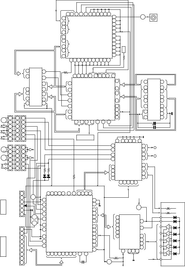
NOTES ON SCHEMATIC DIAGRAM
∙Resistor:
To differentiate the units of resistors, such symbol as K and M are used: the symbol K means 1000 ohm and the symbol M means 1000 kohm and the resistor without any symbol is ohm-type resistor. Besides, the one with “Fusible” is a fuse type.
∙Capacitor:
To indicate the unit of capacitor, a symbol P is used: this symbol P means micro-micro-farad and the unit of the capacitor without such a symbol is microfarad. As to electrolytic capacitor, the expression “capacitance/withstand voltage” is used.
(CH), (TH), (RH), (UJ): Temperature compensation (ML): Mylar type
(P.P.): Polypropylene type
∙Schematic diagram and Wiring Side of P.W.Board for this model are subject to change for improvement without prior notice.
∙The indicated voltage in each section is the one measured by Digital Multimeter between such a section and the chassis with no signal given.
1.In the tuner section, indicates AM indicates FM stereo
2.In the main section, a tape is being played back.
3.In the deck section, a tape is being played back. ( ) indicates the record state.
4.In the power section, a tape is being played back.
5.In the CD section, the CD is stopped.
∙Parts marked with “ ” (
” ( 


 ) are important for maintaining the safety of the set. Be sure to replace these parts with specified ones for maintaining the safety and performance of the set.
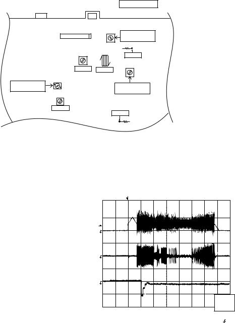
REF. NO |
DESCRIPTION |
POSITION |
|
|
|
SW1 |
OPEN/CLOSE |
ON—OFF |
|
|
|
SW2 |
CLAMP |
ON—OFF |
|
|
|
SW3 |
DISC NUMBER |
ON—OFF |
|
|
|
SW4 |
PICK UP IN |
ON—OFF |
|
|
|
SW601 |
SPAN SELECTOR |
9kHz/50kHz |
|
|
|
SW701 |
ON/STAND-BY |
ON—OFF |
|
|
|
SW702 |
CLOCK |
ON—OFF |
|
|
|
SW703 |
TIMER |
ON—OFF |
|
|
|
SW704 |
KARAOKE MODE |
ON—OFF |
|
|
|
SW705 |
PLAYBACK CONTROL |
ON—OFF |
|
|
|
SW706 |
ON SCREEN DISPLAY |
ON—OFF |
|
|
|
SW707 |
DIGEST |
ON—OFF |
|
|
|
SW709 |
DISC 1 |
ON—OFF |
|
|
|
SW710 |
DISC 2 |
ON—OFF |
|
|
|
SW711 |
DISC 3 |
ON—OFF |
|
|
|
SW712 |
DISC SKIP |
ON—OFF |
|
|
|
SW713 |
OPEN/CLOSE |
ON—OFF |
|
|
|
SW714 |
DIMMER |
ON—OFF |
|
|
|
REF. NO |
DESCRIPTION |
POSITION |
|
|
|
SW715 |
X-BASS/MEMO |
ON—OFF |
|
|
|
SW716 |
EQUALIZER |
ON—OFF |
|
|
|
SW717 |
REVERSE MODE |
ON—OFF |
|
|
|
SW722 |
CD |
ON—OFF |
|
|
|
SW723 |
TAPE |
ON—OFF |
|
|
|
SW724 |
TUNING DOWN |
ON—OFF |
|
|
|
SW725 |
MEMORY/SET |
ON—OFF |
|
|
|
SW726 |
PRESET DOWN |
ON—OFF |
|
|
|
SW727 |
PRESET UP |
ON—OFF |
|
|
|
SW728 |
PLAY |
ON—OFF |
|
|
|
SW729 |
STOP |
ON—OFF |
|
|
|
SW730 |
REVERSE PLAY |
ON—OFF |
|
|
|
SW731 |
REC/PAUSE |
ON—OFF |
|
|
|
SW732 |
TUNING UP |
ON—OFF |
|
|
|
SW733 |
VIDEO/AUX |
ON—OFF |
|
|
|
SW734 |
TUNER |
ON—OFF |
|
|
|
SW801 |
VOLTAGE SELECTOR |
110V—127V |
|
|
220—230-240V |
|
|
|
TYPES OF TRANSISTOR AND LED
|
|
FRONT |
|
FRONT |
|
|
|
|
|
|
|
|||||||
|
|
|
VIEW |
|
|
|
|
|
|
|
||||||||
|
|
|
VIEW |
|
|
FRONT |
||||||||||||
|
|
|
|
|
|
|
|
|
|
|
|
|||||||
|
|
|
|
|
|
|
|
|
|
|
|
|
VIEW |
|||||
|
|
|
|
|
|
|
|
|
|
|
|
|
|
|
|
|
|
|
|
|
|
|
|
|
|
|
|
|
|
|
|
|
|
|
|
|
|
|
E |
|
C |
|
B |
|
|
|
|
|
|
|
|
|||||
|
(S) |
(G) |
(D) |
|
|
|
|
|
|
|
|
|||||||
|
|
B C E |
||||||||||||||||
(1) |
(2) |
(3) |
|
|
||||||||||||||
2SA1015 GR |
|
|
|
KTC3199 GR |
4204UYT7 |
KTC2026 |
||||||||||||
2SC1845 F |
|
|
|
KTC3203 Y |
4204UGT7 |
|
|
|
|
|
|
|
||||||
2SC3203Y |
|
|
|
KTC3265 Y |
4204SRT7 |
|
|
|
|
|
|
|
||||||
AN78L05 |
|
|
|
KTC3194 Y |
|
|
|
|
|
|
|
|
||||||
KIA7805 AP |
|
|
|
KTC3875 GR |
|
|
|
|
|
|
|
|
||||||
KIA7810 AP |
|
|
|
KRC102 M |
|
|
|
|
|
|
|
|
||||||
KTA1266 GR |
|
|
|
KRC102 S |
|
|
|
|
|
|
|
|
||||||
KTA1271 Y |
|
|
|
KRC104 M |
|
|
|
|
|
|
|
|
||||||
KTA1273 Y |
|
|
|
KRC104 S |
|
|
|
|
|
|
|
|
||||||
KTA1274 Y |
|
|
|
KRC107 M |
|
|
|
|
|
|
|
|
||||||
KTA1504 GR |
|
|
|
|
|
|
|
|
|
|
|
|
|
|
|
|||
– 18 –
|
|
|
|
17 |
|
|
|
|
|
~ |
|
|
|
|
|
21 |
|
|
|
|
|
~ |
ICM4 IX0408AW |
|
|
|
|
23 |
|
|
|
|
|
25 |
|
|
|
|
|
30 |
|
|
|
|
|
32 |
|
M3 |
- |
|
|
|
|
CD LOADING |
6 |
6 |
6 |
|
|
|
|
||||
MOTOR |
M |
|
|||
|
|
|
|
||
|
5 |
5 |
5 |
|
|
|
+ |
|
|||
SW3 |
|
|
|
|
|
|
4 |
4 |
4 |
|
|
DISC No. |
|
|
|||
|
|
|
|
|
|
SW2 |
|
3 |
3 |
3 |
|
CLAMP |
|
2 |
2 |
2 |
|
SW1 |
|
|
|||
|
1 |
1 |
1 |
|
|
POEN/CLOSE |
|
|
|||
|
+ |
|
|
CNP4 |
|
M1 |
6 |
6 |
6 |
|
|
M |
|
||||
SPINDLE |
5 |
5 |
5 |
A |
|
MOTOR |
- |
|
|||
M2 |
+ |
4 |
4 |
4 |
|
M |
|
||||
SLED |
3 |
3 |
3 |
B |
|
MOTOR |
- |
|
|||
|
|
|
|
|
|
SW4 |
|
2 |
2 |
2 |
|
PICKUP IN |
|
1 |
1 |
1 |
|
|
|
|
|||
|
|
|
|
CNP3 |
|
|
+10 V |
1 |
|
|
+5 V |
2 |
Q2 |
MAINTO SECTION |
CD-GND |
3 |
|
L-CH |
4 |
|
|
|
A_GND |
5 |
|
|
R-CH |
6 |
Q9 |
|
CNP11 |
||
|
|
||
Q10
|
CNP12 |
||
|
GND |
9 |
|
|
CLAMP SW |
8 |
|
DISPLAYTO SECTION |
CD RES |
7 |
|
CLK |
6 |
||
|
|||
|
DI |
5 |
|
|
DO |
4 |
|
|
CE |
3 |
|
|
DRF |
2 |
|
|
WRG |
1 |
|
|
|
|
|
|
|
|
|
|
|
|
|
|
|
|
|
|
|
|
|
|
|
|
|
|
CD-BK310V |
|
|
|
|
|
|
|
|
|
|
|
|
|
|
|
|
|
|
|
|
|
|
|
JK671 |
|
|
|
|
|
|
|
89 79 |
37 |
33 |
23 |
90 78 73 66 60 59 |
|
|
|
|
|
|
|
VIDEO OUT |
||||||||
|
|
|
|
|
64 |
|
|
|
|
|
|
|
|
|
|||||||||||
|
|
|
|
~ |
EVEN |
No. |
ARCLK |
|
AJN |
ARFS |
|
|
|
|
|
|
|
|
|
QM1 |
|
|
|
||
|
|
|
|
80 |
|
|
|
|
|
|
|
|
|
|
|
53 |
|
|
|
|
|
|
|
|
|
|
|
|
|
86 |
|
|
|
|
|
|
|
|
|
|
|
|
|
|
|
|
|
|
|
|
|
|
|
|
|
|
|
|
|
|
|
|
|
|
|
|
32 |
|
|
|
|
|
|
|
|
|
|
|
|
|
|
92 |
|
|
|
|
|
|
|
|
|
|
|
|
|
|
|
|
|
|
|
|
|
|
|
|
|
EVEN |
No. |
|
|
|
|
|
|
|
|
|
16 |
|
|
|
|
|
|
|
|
|
|
|
|
|
|
~ |
|
|
|
|
|
|
|
|
|
|
|
|
|
|
|
|
|
|
|||
|
|
|
|
|
|
|
|
|
|
|
|
|
|
|
|
|
|
|
|
|
|
|
|
|
|
|
|
|
|
98 |
|
|
|
|
|
|
|
|
|
|
|
5 |
|
|
|
|
|
|
|
|
|
|
|
|
|
8 |
|
|
|
|
|
ICM3 |
|
|
|
|
100 |
|
|
|
|
|
|
|
|
|
|
|
|
|
|
|
|
|
|
ES3889F |
|
|
|
|
|
|
|
|
|
|
|
|
|
||||
|
|
|
|
81 |
ODD |
No. |
VCD COMPANION CHIP |
|
91 |
|
|
|
|
|
|
|
|
|
|||||||
|
|
|
|
~ |
|
|
|
|
|
|
|
|
|
77 |
|
|
|
|
|
|
|
|
|
||
|
|
|
|
85 |
|
|
|
|
|
|
|
|
|
|
|
75 |
CNP1 |
|
|
|
|
|
|
|
|
|
|
|
|
~ |
ODD |
No. |
|
|
|
|
|
|
|
|
|
|
|
|
|
|
|
|
|
||
|
|
|
|
93 |
|
|
|
|
|
|
|
|
|
|
|
72 |
|
|
|
|
|
|
|
|
|
|
|
|
|
|
|
|
|
|
|
|
|
|
|
|
|
|
|
|
|
|
|
|
|
|
|
|
|
|
|
99 |
|
|
|
|
|
|
|
|
|
|
|
63 |
|
|
|
|
|
|
|
|
|
|
|
|
|
|
|
|
|
|
|
|
|
|
|
|
|
|
|
|
|
|
|
|
|
|
|
|
|
|
|
|
6 |
|
1 |
25 26 31 41 43 51 56 57 62 |
|
|
|
|
|
|
|
|
|
|
|||||||
OE_ 24 |
|
|
|
DSO C |
|
|
|
|
|
|
|
|
|
|
|
|
|
|
|
|
|
|
|
|
|
|
|
|
|
|
|
|
|
|
|
|
|
|
|
|
|
|
|
|
|
|
|
|
|
||
CE_ 22 |
|
|
|
|
100 80 50 30 47 ~ 45 44 43 41 ~ 32 |
|
|
|
|
|
|
|
|
|
|||||||||||
|
|
|
|
|
|
|
|
|
|
|
|
|
|
|
|
|
|
|
|
|
|
|
|
||
|
15 |
|
|
|
55 |
|
|
|
|
|
|
|
|
|
|
12 |
|
|
|
|
19 |
|
|
22 |
|
|
|
|
|
|
|
|
|
|
|
|
|
|
|
|
|
|
|
|
|
|
|
||||
EPROM |
|
|
|
|
|
|
|
|
|
|
|
|
|
|
~ |
|
|
|
|
~ |
ICM1 |
1625635T DRAM |
~ |
||
1 |
|
|
|
~ |
|
|
|
|
|
|
|
|
|
|
|
|
|
|
|
|
~ |
~ |
|||
|
~ |
|
|
|
|
|
|
|
|
|
|
|
|
|
|
4 |
|
|
|
|
16 |
|
|
26 |
|
|
13 |
|
|
|
62 |
|
|
|
|
|
|
ICM2 |
|
|
|
|
|
|
|
|
10 |
|
|
31 |
|
|
12 |
|
|
|
64 LOE# |
|
|
ES3880F |
|
|
28 |
|
|
|
|
~ |
|
|
~ |
||||||
|
|
|
|
|
|
|
|
|
~ |
|
|
|
|
6 |
|
|
34 |
||||||||
|
~ |
|
|
|
|
|
|
|
VCD PROCESSOR CHIP |
|
|
|
|
|
|
|
|||||||||
|
2 |
|
|
|
|
|
|
|
|
|
|
|
|
|
|
|
|||||||||
|
|
|
|
65 LROMCE# |
|
|
|
|
|
|
13 |
|
|
|
|
5 |
|
|
36 |
||||||
|
|
|
|
|
|
|
|
|
|
|
|
|
|
|
|
|
|||||||||
|
|
|
|
|
66 LSC1# |
|
|
|
|
|
|
81 |
|
|
|
|
2 |
|
|
39 |
|||||
|
|
|
|
|
68 |
|
|
|
|
|
|
|
|
|
|
51 |
|
|
|
|
20 |
|
|
21 |
|
|
|
|
|
|
|
|
|
|
|
|
|
|
ARCLK |
|
31 |
|
|
|
|
|
|
35 |
|||
|
|
|
|
|
|
|
|
|
|
|
|
|
AJN |
ARFS |
|
|
|
|
|
|
|
||||
|
|
|
|
|
79 |
|
|
|
|
|
|
|
|
1 |
|
|
|
|
1 |
|
|
40 |
|||
|
|
|
|
|
|
|
82 ~ 87 |
88 ~ 91 |
93 |
94 |
95 |
|
|
|
|
|
|
|
|
|
|
||||
|
|
|
|
|
|
|
|
TO ICM3 |
|
|
|
|
|
|
|
|
|
|
|
|
|
|
|
||
|
|
|
|
|
|
|
|
17, 19, 21, 22PIN |
|
|
|
|
35 ~ 29 22 21 14 ~ 8 |
|
|
|
|
||||||||
|
|
|
|
|
|
|
|
|
|
|
|
|
|
|
|
|
|
|
|
|
|||||
|
|
|
|
|
|
|
|
|
|
|
|
|
|
|
|
39 CAM. M+ |
|
|
|
SP- |
27 |
|
B |
|
|
|
|
|
|
|
|
|
|
|
|
|
|
|
|
|
|
38 CAM. M- |
|
M63001FP FOCUS/TRACKING/ |
DRIVERSPIN/SLED |
SP+ |
26 |
|
|
||
|
|
|
|
|
|
|
|
|
|
|
|
|
|
|
|
IC3 |
|
|
|
||||||
|
|
|
|
|
|
|
|
|
|
|
|
|
|
|
|
42 |
CAM. M+ |
SL+ |
16 |
|
A |
|
|||
|
|
|
|
|
|
|
|
|
|
|
|
|
|
|
|
|
|
|
|
|
|||||
|
|
|
|
|
|
|
|
|
|
|
|
|
|
|
|
|
|
|
|
|
SL- |
15 |
|
|
|
|
|
|
|
|
|
|
|
|
|
|
|
|
|
|
|
41 |
CAM. M- |
|
|
|
|
|
|
||
|
|
|
|
|
|
|
|
|
|
|
|
|
|
|
|
|
|
|
|
|
|
|
|
||
|
|
|
|
|
|
|
|
|
|
|
|
|
|
|
|
25 SPDO |
|
|
|
TR- |
7 |
|
|
|
|
|
|
|
|
|
|
|
|
|
|
|
|
|
|
|
|
|
|
|
TR+ |
6 |
|
|
|
||
|
|
|
|
|
|
|
|
|
|
|
|
|
|
|
|
17 SLDO |
|
|
|
|
|
|
|||
|
|
|
|
|
|
|
|
|
|
|
|
|
|
|
|
|
|
|
|
5 |
|
|
|
||
|
|
|
|
|
|
|
|
|
|
|
|
|
|
|
|
2 |
FD |
|
|
|
FO- |
|
|
|
|
|
|
|
|
|
|
|
|
|
|
|
|
|
|
|
|
|
|
|
|
4 |
|
|
|
||
|
|
|
|
|
|
|
|
|
|
|
|
|
|
|
|
1 |
TO |
|
|
|
FO+ |
|
|
|
|
|
|
|
|
|
|
|
|
|
|
|
|
|
|
|
|
|
|
|
|
|
|
|
|
||
|
|
|
|
|
|
|
|
|
|
|
|
|
|
|
|
|
18 40 24 23 28 |
|
|
|
|
||||
|
|
56 55 54 35 57 ~ 59 |
33 26 25 24 23 |
|
|
|
|
|
-5 V |
|
|
|
|
|
|
|
|||||||||
|
|
|
|
|
|
CONT5 |
|
SLDO SPDO |
FDO |
TDO |
|
|
|
|
|
|
|
+3.3 V |
|
|
|
||||
|
40 |
|
|
|
|
|
|
|
|
|
|
|
|
|
|
|
|
|
|||||||
|
|
|
|
|
|
|
|
|
|
|
19 |
|
|
|
|
|
|
|
|
|
|
|
|
|
|
|
30 CONT2 |
|
|
|
|
|
|
|
|
|
3 |
|
|
|
|
|
LASER |
|
|
|
|
TRACKING COIL |
|||
|
|
|
|
|
|
|
|
|
|
|
|
|
|
|
|
|
|
Q3 |
|
|
|
||||
|
31 CONT3 |
|
|
|
|
|
|
|
|
TE 16 |
|
|
|
|
|
DRIVER |
|
|
|
FOCUS COIL |
|||||
|
|
|
|
|
|
|
|
|
|
|
FE 15 |
|
|
|
|
|
|
|
|
|
|
|
|
||
|
32 CONT4 |
|
|
|
|
|
|
|
|
|
|
|
|
|
|
|
|
|
|
|
|
|
|||
|
41 RCHO |
|
|
IC2 |
|
|
|
RFEV 14 |
|
|
|
|
22 RFEV |
|
|
|
|
|
|
|
|||||
|
|
|
|
|
|
|
HFL |
7 |
|
|
|
|
21 FE- |
|
|
LDD |
8 |
|
|
|
|||||
|
|
|
|
LC78636E |
|
|
|
|
|
|
|
|
|
|
|||||||||||
|
47 |
RVSS |
|
|
|
|
|
|
|
|
20 FE |
|
LA9235M SERVOAMP. |
|
|
|
|
|
|
||||||
|
SERVO/SIGNAL XVDD 50 |
|
|
|
|
|
|
|
7 |
|
|
|
|||||||||||||
|
46 |
|
|
|
V+3.3 |
|
19 TE- |
IC1 |
|
PD |
|
|
|
||||||||||||
|
LVSS |
|
CONTROL |
RVDD 49 |
|
|
|
18 TE |
FIN2 |
2 |
|
|
|
||||||||||||
|
|
|
|
|
|
|
|
|
|
|
|
|
|
||||||||||||
|
|
|
|
LVDD 44 |
|
|
|
|
|
|
|
|
|
|
|
|
|||||||||
|
53 LCHO |
|
|
|
|
|
|
|
|
|
|
|
17 HFL |
|
|
TIN2 |
4 |
|
|
|
|||||
|
|
|
|
|
|
|
|
|
VDD 36 |
|
|
|
|
|
|
|
|
|
|||||||
|
|
|
|
|
|
|
|
|
|
|
|
|
|
|
|
|
|
TIN1 |
3 |
|
|
|
|||
|
76 CONT7 |
|
|
|
|
|
|
|
ADAVDD 18 |
|
|
|
|
|
|
|
|
|
|
||||||
|
|
|
|
|
|
|
|
|
|
|
|
|
|
|
|
|
|
|
|
|
|||||
|
75 CONT6 |
|
|
WRQ RES |
|
|
|
XOUT |
VVDD |
5 |
|
|
|
|
|
|
|
FIN1 |
1 |
|
|
|
|||
|
DI DO |
INT |
DEF |
|
XIN |
VDD 73 |
|
|
|
|
|
|
|
|
|
|
|||||||||
|
|
CE CL |
|
|
|
|
|
|
|
|
|
|
|
||||||||||||
|
|
|
|
|
|
|
|
|
|
|
|
|
|
|
|
|
|
|
|
|
|
|
|||
|
|
65 66 67 68 69 70 71 72 |
|
52 |
51 |
|
|
+5 V |
|
|
30 |
|
23 11 |
9 |
|
|
|
|
|||||||
|
|
|
|
|
|
|
|
|
|
|
|
|
|
|
|
|
|
||||||||
|
|
|
|
|
|
|
|
|
|
|
|
|
|
|
Q4 |
|
|
|
|
|
|
+5 V |
|
|
|
|
|
|
|
|
|
|
|
|
|
|
|
|
|
|
|
|
|
|
|
|
|
|
|
|
|
|
|
|
|
|
|
|
|
|
XL2 |
|
CONSTANT |
|
|
|
|
|
|
|
|
|
|
PICKUP UNIT |
|||
|
|
|
|
|
|
|
|
|
|
VOLTAGE |
|
|
|
|
|
|
|
|
|
|
|
||||
|
|
|
|
|
|
|
|
|
|
|
|
|
|
+3.3 V |
|
|
|
|
|
|
|
||||
|
|
|
|
|
|
|
|
|
|
|
|
|
|
|
|
|
|
|
|
|
|
|
|
||
Figure 19 BLOCK DIAGRAM (1/3)
– 19 –
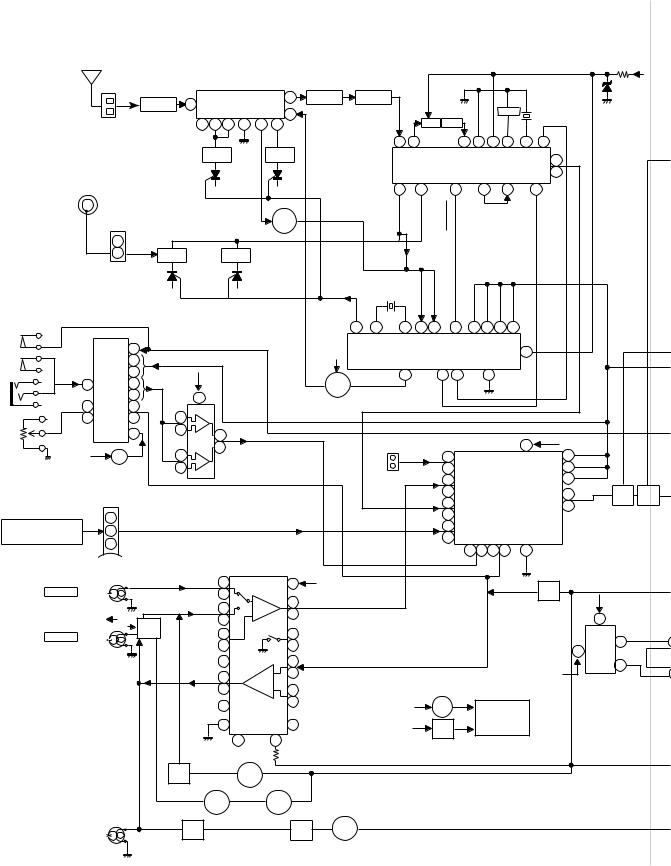
CD-BK310V |
|
|
|
|
|
|
|
|
|
|
|
|
|
|
|
|
|
|
|
|
|
|
|
|
|
|
|
|
|
|
|
|
|
|
|
|
FM |
|
|
|
|
|
|
|
|
|
|
|
|
|
|
|
|
|
|
|
|
|
|
|
|
|
|
|
|
|
|
|
|
|
|
ANTENNA |
|
|
|
|
|
|
|
|
|
|
|
|
|
|
|
|
|
|
|
|
|
|
|
|
|
|
|
|
|
|
+B4 |
||||
|
|
|
|
|
|
|
|
|
|
|
|
|
|
|
|
|
|
|
|
|
|
|
|
|
|
|
|
|
|
|
|
|
|
||
|
|
|
|
|
|
|
|
|
|
|
|
|
|
|
FM IF |
|
|
|
|
|
|
|
|
|
|
10.7MHz |
|
|
|
|
|
|
|||
|
|
|
|
|
|
|
|
IC301 |
|
|
6 |
T302 |
|
CF303 |
|
|
|
|
|
|
|
|
|
|
|
|
|
|
|
|
|
||||
|
|
|
|
BF301 |
|
1 |
TA7358AP |
|
|
|
|
|
|
|
|
|
|
|
|
|
|
CF351 |
|
|
|
|
|
|
|
||||||
|
|
|
|
B.P.F |
|
FM FRONT END 9 |
|
|
|
|
|
|
450kHz |
|
|
|
|
X351 |
|
|
|
|
|
||||||||||||
|
|
SO302 |
|
2 |
3 |
4 |
5 |
7 |
8 |
|
|
|
|
|
|
T351 CF352 |
|
|
|
|
|
|
456kHz |
|
|
|
|
|
|||||||
|
|
FM ANTENNA |
|
|
|
|
|
|
FM |
OSC |
|
|
|
|
|
|
|
AM IF |
|
|
|
|
|
|
|
|
|
|
|
|
|
|
|||
|
|
TERMINAL |
|
FM |
|
|
|
|
|
|
|
|
IC303 |
|
1 |
2 |
|
|
4 |
|
5 |
9 |
8 |
17 |
13 |
|
|
|
|
|
|||||
|
|
|
|
|
|
|
|
|
|
|
|
|
|
|
|
|
AM MIX |
|
AM IF GND FM+B FM VCOMO/ST |
|
|
|
|
|
|||||||||||
|
|
|
|
|
|
L312 |
|
|
|
|
T301 |
|
LA1832S |
|
|
|
|
|
|
||||||||||||||||
|
|
|
|
|
|
RF |
|
|
|
|
|
|
|
|
|
FM IFDET. |
|
|
|
|
|
|
|
|
|
DET |
|
L 14 |
|
|
|
|
|
||
|
|
|
|
|
|
|
|
|
|
|
|
|
|
FM |
|
|
|
|
|
|
|
|
|
|
|
|
|
|
|
|
|
||||
|
|
|
|
|
|
|
|
|
|
|
|
|
|
|
FM MPX./ |
|
|
|
|
|
|
FM/AM |
|
|
R 15 |
|
|
|
|
|
|||||
AM LOOP |
|
|
|
|
|
|
|
|
|
|
OSC |
AM IF MPX. |
|
|
|
|
|
|
|
OUT |
MPXIN |
FM/AM |
|
|
|
|
|
||||||||
|
|
|
|
|
|
|
|
|
|
|
|
23 |
21 |
|
7 |
|
|
|
|
|
|
|
|||||||||||||
ANTENNA |
|
|
|
|
|
|
|
|
|
|
|
|
|
|
|
|
|
|
18 |
|
16 |
|
12 |
|
|
|
|
|
|||||||
|
|
|
|
|
AM TRACKING |
|
|
OSC BUFF |
|
|
|
OSCAMIN |
RFAMIN |
|
STEREO |
|
|
|
|
|
|
|
|
|
|
|
|
|
|||||||
|
|
|
|
|
|
|
|
|
|
|
|
|
|
|
|
|
|
|
|
|
|
|
|
|
|
|
|
|
|
|
|
||||
|
|
|
CNP301 |
|
|
|
|
|
|
|
|
Q302 |
|
|
|
|
|
|
|
|
|
|
|
|
|
|
|
|
|
|
|
|
|
||
|
|
|
|
|
|
|
|
|
|
|
|
|
|
|
|
|
|
|
|
|
|
|
|
|
|
|
|
|
|
|
|
|
|
||
|
|
|
1 |
|
|
|
|
|
|
|
|
|
|
|
|
|
|
|
|
|
|
|
|
|
|
|
|
|
|
|
|
|
|
|
|
|
|
|
2 |
T303 |
|
|
T306 |
AM BAND |
|
|
|
|
|
|
|
|
|
|
|
|
|
|
|
|
|
|
|
|
|
||||||
|
|
|
|
|
|
COVERAGE |
|
|
|
|
|
|
|
|
|
|
|
|
|
|
|
|
|
|
|
|
|
||||||||
|
|
|
|
|
|
|
|
|
|
|
|
|
|
|
|
|
|
|
|
|
|
|
|
|
|
|
|
|
|
|
|
||||
|
|
|
|
|
|
|
|
|
|
|
|
|
|
|
VT |
|
X352 |
|
|
|
|
|
|
|
|
|
|
|
|
|
|
|
|
||
|
|
|
ICK1 |
|
|
|
|
|
|
|
|
|
|
|
|
4.5MHZ |
|
|
|
|
|
|
|
|
|
|
|
|
|
|
|
|
|||
|
|
|
|
|
|
|
|
|
|
|
|
|
|
|
|
|
|
|
|
|
|
|
|
|
|
|
|
|
|
|
|
|
|||
|
|
|
|
|
|
|
|
|
|
|
|
|
|
|
|
|
|
|
|
|
|
|
CE |
|
DI |
CLK |
DO |
|
|
|
|
|
|
|
|
|
|
M65856SP |
|
|
|
|
|
|
|
|
|
|
|
|
|
|
|
|
|
|
|
|
|
|
|
|
|
|
|
||||||
JK1 |
|
MIC AMP. |
|
|
|
|
|
|
|
|
|
|
|
|
20 |
1 |
22 |
15 16 |
11 |
3 |
4 |
5 |
6 |
|
|
|
|
|
|
|
|||||
MIC |
|
|
|
|
|
|
|
|
|
|
|
|
|
|
|
|
|
|
|
|
|
|
|
||||||||||||
|
|
|
|
|
|
|
|
|
|
|
|
|
|
|
|
|
|
OSC |
IC302 |
|
|
|
|
|
|
|
|
|
|
|
|
||||
|
|
|
LATCH 40 |
|
|
|
|
|
|
|
|
|
|
|
|
|
|
|
LC72131 |
|
|
|
|
|
17 |
|
|
|
|
|
|
||||
|
|
|
CLK 41 |
|
|
|
|
|
|
|
|
|
|
+B4 |
|
|
|
PLL(TUNER) |
|
|
|
|
|
|
|
|
|
|
|||||||
|
|
|
|
|
|
|
|
|
|
|
|
|
|
|
|
|
|
|
|
|
|
|
|
|
|
|
|||||||||
|
|
|
|
|
|
|
|
|
|
|
|
+B |
|
|
|
|
FM/AM MO/ST |
|
|
|
|
|
|
|
|
|
|
|
|||||||
|
|
|
DATA 42 |
|
+B4 |
|
|
|
|
|
|
|
|
|
|
|
|
|
|
|
|
|
|
|
|
|
|
||||||||
MIC IN |
|
|
|
|
|
|
|
|
|
FM |
|
FM |
|
7 |
|
9 |
10 |
|
|
21 |
|
|
|
|
|
|
|
|
|||||||
|
LOUT 36 |
|
|
|
|
|
|
|
|
|
|
|
|
|
|
|
|
|
|
|
|
|
|||||||||||||
|
9 |
|
|
|
|
|
|
|
|
|
|
|
Q360 |
|
|
|
|
|
|
|
|
|
|
|
|
|
|
|
|
|
|
|
|||
|
|
|
ROUT 35 |
|
8 |
|
|
|
|
|
|
|
|
CONSTANT |
|
|
|
|
|
|
|
|
|
|
|
|
|
|
|
|
|
|
|||
|
12 |
|
|
31 |
|
|
|
|
|
|
|
|
|
|
|
|
|
|
|
|
|
|
|
|
|
|
|
|
|
|
|
||||
|
|
L IN |
|
|
|
|
|
|
|
|
|
|
|
|
|
|
|
|
|
|
|
|
|
|
|
|
|
|
|
|
|||||
|
|
|
|
|
|
|
|
|
|
|
|
VOLTAGE |
|
|
|
|
|
|
|
|
|
|
|
|
|
|
|
|
|
|
|||||
|
13 |
|
R IN 32 |
5 |
|
|
|
|
|
|
|
|
|
|
|
|
|
|
|
|
|
|
|
|
|
|
|
|
|
|
|
||||
|
|
|
|
|
|
|
|
|
|
|
|
|
|
|
|
|
|
|
|
|
|
|
|
|
|
|
|
|
|
|
|
||||
VRK1 |
|
|
VCC 23 |
6 |
|
|
7 |
L |
|
|
|
|
|
|
|
|
|
|
|
|
|
|
|
|
|
|
|
|
|
|
|
|
|
||
|
|
|
|
|
|
|
|
|
|
|
|
JK601 |
|
|
|
|
|
|
|
|
|
|
+B4 |
|
|
|
|
|
|||||||
MIC |
|
|
|
|
|
|
|
1 |
R |
|
|
|
|
|
|
|
|
|
|
|
|
|
|
|
23 |
|
|
|
|
|
|||||
|
|
|
|
|
|
|
|
|
|
|
|
|
|
|
|
|
|
|
|
|
|
|
|
|
|
|
|
||||||||
VOLUME |
+B5 |
QK1 |
|
2 |
|
|
|
|
|
|
|
|
|
|
|
|
L |
VIDEO IN |
9 |
|
|
|
|
|
|
|
DI |
1 |
|
|
|
|
|||
|
|
|
|
|
|
|
|
|
|
|
|
|
|
|
AUX |
L |
|
|
|
|
|
|
|
|
|
|
|
||||||||
|
|
|
|
|
3 |
|
|
|
|
|
|
|
|
|
|
|
|
R |
|
|
R 16 |
|
|
|
|
|
|
|
CE |
2 |
|
|
–20dB |
||
|
|
|
|
|
|
|
|
|
|
|
|
|
|
|
|
|
|
|
|
|
|
|
|
|
|
|
|
|
|
CLK 24 |
|
|
|||
|
|
|
|
|
|
|
|
|
|
|
|
|
|
|
|
|
|
|
|
TAPE L 10 |
|
|
|
|
IC601 |
|
|
|
ATT |
||||||
|
|
|
|
|
|
ICK2 |
|
|
|
|
|
|
|
|
|
|
|
|
|
R 15 |
|
|
|
|
|
|
21 R |
|
Q603 |
Q605 |
|||||
|
|
|
CNS11 |
|
KIA4558P |
|
|
|
|
|
|
|
|
|
|
TUNER |
L 11 |
|
|
|
LC75341 |
|
|
L |
|
Q604 |
Q606 |
||||||||
|
|
|
|
|
|
|
|
|
|
|
|
|
|
|
AUDIO PROCESSOR 4 |
|
|
SYSTEM |
|||||||||||||||||
|
|
|
|
|
OPE AMP. |
|
|
|
|
|
|
|
|
|
|
|
|
R 14 |
|
|
|
||||||||||||||
|
|
|
1 |
|
|
|
|
|
|
|
|
|
|
|
|
|
|
|
|
|
|
|
|
|
|
|
|
|
MUTE |
||||||
FROM VIDEO |
|
|
|
|
|
|
|
|
|
|
|
|
|
|
|
|
|
|
CD L 12 |
|
|
|
|
|
|
|
|
|
|
|
|
||||
|
|
2 |
|
|
|
|
|
|
|
|
|
|
|
|
|
|
|
|
|
|
|
|
|
|
|
|
|
|
|
|
|
||||
CD SECTION |
|
|
|
|
|
|
|
|
IC101 |
|
|
|
|
|
|
|
|
R 13 |
|
|
|
|
|
|
|
|
|
|
|
|
|
||||
CNP11 |
|
|
3 |
|
|
|
|
|
|
|
|
|
|
|
|
|
|
|
|
|
|
|
|
|
|
|
|
|
|
|
|||||
|
|
|
|
|
|
PLAYBACK AND |
|
|
|
|
|
|
|
|
|
7 |
|
18 8 17 |
3 |
|
|
|
|
|
|
||||||||||
|
|
|
|
|
|
|
|
|
|
|
|
|
|
|
|
|
|
|
|
|
|
|
|||||||||||||
|
|
|
|
|
|
|
|
RECORD/ |
|
|
|
|
|
|
MIC |
|
|
L |
|
R |
|
|
|
|
|
|
|
|
|
||||||
|
|
|
|
|
|
|
PLAYBACK AMP. |
|
|
|
|
|
|
|
|
|
|
|
|
|
|
|
|
|
|
|
|
|
|||||||
|
|
|
|
|
|
L(T1) |
1 |
|
|
|
|
|
13 |
+B4 |
|
|
|
|
|
|
|
|
|
|
|
|
|
|
Q121 |
|
|
|
REC/PLAY |
||
TAPE 1 |
L-CH |
|
|
|
|
|
|
|
|
|
|
|
|
|
|
|
|
|
|
|
|
|
|
|
|
|
|||||||||
|
|
R(T1) |
24 |
|
|
|
|
|
|
|
|
|
|
|
|
|
|
|
|
|
|
|
|
|
|
|
|
||||||||
|
|
|
|
|
P.B |
4 |
L PB |
|
|
|
|
|
|
|
|
|
|
|
|
|
|
Q122 |
|
|
+B4 |
|
|||||||||
P.B. HEAD R-CH |
SWITCHING |
L(T2) |
2 |
|
|
|
|
|
|
|
|
|
|
|
|
|
|
|
|
|
|
|
MUTING |
|
|
||||||||||
|
|
|
|
|
|
|
|
|
21 |
R |
|
|
|
|
|
|
|
|
|
|
|
|
|
|
|
|
|
|
|||||||
|
|
|
|
|
|
|
|
|
|
|
|
|
|
|
|
|
|
|
|
|
|
|
|
|
|
|
|
|
|||||||
|
|
|
REC |
|
R(T2) |
23 |
|
|
|
|
|
|
|
|
|
|
|
|
|
|
|
|
|
|
|
|
|
|
8 |
|
|
||||
|
|
|
|
|
|
|
|
|
|
|
|
|
|
|
|
|
|
|
|
|
|
|
|
|
|
|
|
|
|
||||||
|
|
|
P.B. |
Q103- |
|
|
|
|
|
|
|
|
|
|
|
|
|
|
|
|
|
|
|
|
|
|
|
|
|
|
|
|
|
|
|
TAPE 2 |
L-CH |
Q106 |
|
L NF |
3 |
|
|
|
|
|
5 |
|
|
|
|
|
|
|
|
|
|
|
|
|
|
|
|
|
|
IC702 |
|
|
|||
|
|
|
|
|
|
|
|
|
|
|
|
|
|
|
|
|
|
|
|
|
|
|
|
|
1 |
|
|||||||||
|
R-CH |
|
|
R NF |
22 |
|
|
|
|
|
20 |
|
|
|
|
|
|
|
|
|
|
|
|
|
|
|
|
|
|
|
|
||||
REC. P.B. HEAD |
|
|
|
|
|
|
|
|
|
|
|
|
|
|
|
|
|
|
|
|
|
|
|
|
|
|
4 |
IC703 |
|
IC70 |
|||||
|
|
|
|
|
|
|
|
|
|
|
H/N |
|
|
|
|
|
|
|
|
|
|
|
|
|
|
|
|
|
|
|
|||||
|
|
|
|
|
|
|
|
|
|
|
|
|
|
|
|
|
|
|
|
|
|
|
|
|
|
|
|
|
|
|
|
||||
|
|
|
AC BIAS |
POP REDUCE |
6 |
|
T1/T2 |
|
|
|
7 |
L REC |
|
|
|
|
|
|
|
|
|
|
|
|
|
|
|
|
|
|
7 |
IX041 |
|||
|
|
|
|
|
|
L REC |
9 |
|
REC |
|
|
|
18 |
R |
|
|
|
|
|
|
|
|
|
|
|
|
|
|
–B2 |
|
|
KIA4558P |
|
||
|
|
|
|
|
|
|
|
|
|
|
|
|
|
|
|
MOTOR |
|
|
|
|
|
|
|
|
|
|
|||||||||
|
|
|
|
|
|
R REC 16 |
|
|
|
|
|
8 |
L NF |
|
|
|
|
|
|
|
|
|
|
|
|
|
OPE AMP. |
|
|||||||
|
|
|
|
|
|
|
|
|
|
|
|
|
|
|
DRIVER |
|
|
|
|
|
|
|
|
|
|
|
|
||||||||
|
|
|
|
|
|
REF 14 |
|
|
|
|
|
17 |
R NF |
|
|
|
+B3 |
Q708 |
|
|
|
|
TAPE |
|
|
|
|
|
|
|
|||||
|
|
|
|
|
|
|
|
|
|
|
|
|
|
|
|
|
|
|
|
|
|
|
|
|
|
|
|||||||||
|
|
|
|
|
|
|
|
|
|
|
|
|
|
|
|
|
|
|
|
|
|
|
|
|
|
|
|
|
|
|
|
|
|
||
|
|
|
|
|
|
|
|
|
|
NOR/ |
|
|
|
|
ALC |
|
|
|
|
|
|
|
|
|
|
MECHANISM |
|
|
|
|
|
|
|||
|
|
|
|
|
|
|
|
12 |
|
|
T1/T2 |
10 |
|
|
|
+B3 |
|
Q704 |
|
|
|
ASS'Y |
|
|
|
|
|
|
|
||||||
|
|
|
|
|
|
|
|
|
|
HIGH |
|
|
|
|
|
|
|
Q705 |
|
|
|
|
|
|
|
|
|
|
|
|
|
||||
|
|
|
|
|
|
|
|
|
|
15 |
|
|
19 |
|
|
|
|
|
|
|
|
|
|
|
|
|
|
|
|
|
|
|
|
||
|
|
|
|
|
|
|
|
|
|
|
|
|
|
|
|
|
|
SOLENOID |
|
|
|
|
|
|
|
|
|
|
|
|
|||||
|
|
|
|
|
|
|
|
|
|
|
|
|
|
|
|
|
|
|
|
|
|
|
|
|
|
|
|
|
|
|
|
||||
|
|
|
|
|
SWITCHING |
SWITCHING |
|
|
|
|
|
|
DRIVER |
|
|
|
|
|
|
|
|
|
|
|
|
T1/T2 |
|||||||||
|
|
|
|
|
|
|
|
|
|
|
|
|
|
|
|
|
|
|
|
|
|
|
|
|
|
||||||||||
|
|
|
|
|
Q107 |
|
|
|
Q111 |
|
|
|
|
|
|
|
|
|
|
|
|
|
|
|
|
|
|
|
|
|
|
|
|
||
|
|
|
|
|
Q108 |
|
|
|
|
|
|
|
|
|
|
|
|
|
|
|
|
|
|
|
|
|
|
|
|
|
|
|
|||
|
|
|
|
|
|
|
|
|
|
|
|
|
|
|
|
|
|
|
|
|
|
|
|
|
|
|
|
|
|
|
|
|
|
||
|
|
|
|
|
|
|
Q109 |
SWITCHING |
Q110 |
|
BIAS |
|
|
|
|
|
|
|
|
|
|
|
|
|
|
|
|
|
|
||||||
|
|
|
|
|
|
|
|
|
|
SWITCHING |
|
|
|
|
|
|
|
|
|
|
|
|
|
|
|
|
|
|
|||||||
|
|
|
|
|
|
|
|
|
|
|
|
|
|
|
|
|
|
|
|
|
|
|
|
|
|
|
|
|
|
|
|
||||
ERASE |
BIAS Q128 |
Q124 |
Q126 |
BIAS |
OSC L104 |
L103 |
|
|
|
HEAD |
|
|
|
|
Figure 20 BLOCK DIAGRAM (2/3)
– 20 –
CD-BK310V
+B4 |
FL701 |
FL DISPLAY
1 2 3 |
4 ~ 12 |
13 ~ 18 |
19 ~ 24 |
25 ~ 36 |
37 38 39 |
JOG701 |
|
|
|
|
|
||||||
|
|
|
|
|
|
JOG |
|
|
|
Q701-Q703 |
|
|
|
|
|
|
|
|
Q710-Q712 |
|
|
+B5 |
|
|
RX701 |
|
|
|
|
|
|
|
1 |
REMOTE |
3 |
|
|
|
|
|
|
|
SENSOR |
|
|
|
|
|
|
|
|
|
|
|
|
|
|
|
|
|
|
2 |
|
|
+B5 |
|
|
|
|
|
|
|
|
|
|
|
|
|
|
|
|
|
|
|
|
|
|
|
|
|
|
|
|
61 |
57 56 55 54 53 52 51 50 49 48 |
46 45 44 43 42 41 40 |
|
|
|
|
|
||||||
|
|
|
|
|
|
|
67 |
|
|
|
|
|
|
VDD |
|
39 |
|
|
|
|
|
|
|
|
|
|
|
- |
|
|
|
61 |
|
|
|
38 |
KEY |
|
|
||
|
|
|
|
|
|
|
78 |
|
|
|
|
|
|
|
|
|
|
|
||
|
|
|
|
|
|
|
|
|
KARAOKE LATCH |
|
|
|
|
37 |
SW701-SW707 |
|||||
|
|
|
|
|
|
|
- |
|
|
|
IC701(1/2) |
|
|
+B5 |
BU2092F |
|
|
|||
|
|
|
|
|
|
|
79 VLOAD |
|
|
|
|
|
|
|
SW709-SW717 |
|||||
|
|
|
|
|
|
|
80 |
|
|
|
|
|
|
|
|
36 |
SW722-SW734 |
|||
|
|
|
|
|
|
|
|
|
|
|
|
|
|
|
35 |
IC704 |
|
|
||
|
|
|
|
|
|
|
|
|
|
|
|
|
IX0411AW |
|
|
|
|
|||
|
|
|
|
|
|
|
85 |
|
|
|
|
|
|
AVDD 34 |
INPUT/OUTPUT +B6 |
|||||
|
|
|
|
|
|
|
|
|
|
|
|
SYSTEM MICROCOMPUTER |
|
|||||||
|
|
|
|
|
|
|
86 |
|
|
|
|
33 |
EXPANDER |
|
||||||
|
|
|
|
|
|
|
|
|
|
|
|
|
|
|
- |
1 |
|
|
|
|
|
|
|
|
|
|
|
- |
|
|
|
|
|
|
|
|
|
|
|
||
|
|
|
|
|
|
|
91 |
|
|
|
|
|
|
|
|
31 |
2 |
|
|
18 |
|
|
|
|
|
|
|
100VDD |
|
|
|
|
RESET |
VDD |
|
CE CLK DI DO |
23 |
IC704 |
|||
|
|
|
|
|
|
|
|
|
|
|
|
58 |
|
4 |
|
|
||||
|
|
|
|
|
|
|
92 |
|
|
|
|
|
|
|
|
22 |
3 |
|
|
|
|
|
|
|
|
|
|
|
|
|
|
|
|
|
|
|
|
|
|
||
|
|
|
|
|
|
|
1 |
2 |
4 |
5 |
6 |
7 - 9 10 11 12 13 15 16 17 |
- 20 21 22 23 24 |
|
|
|
|
|
||
|
|
|
|
|
|
|
+B5 |
|
|
|
|
|
+B5 |
|
|
TO CD |
|
|
|
|
|
|
|
|
|
|
|
|
|
|
|
XL701 |
|
|
|
|
|
||||
|
|
|
|
|
|
|
|
|
|
|
|
|
|
|
SECTION |
|
|
|
||
|
|
|
|
|
|
|
|
|
4.194304MHz |
|
|
|
|
+B3 |
|
|
||||
|
|
|
|
|
|
|
|
|
|
|
RESET Q709 |
+B5 |
|
|
|
|
JK670 |
|||
|
|
|
|
|
|
|
|
|
|
|
|
|
|
|
|
|||||
|
|
|
|
|
|
Q906 |
|
|
|
|
|
|
SPAN |
|
|
|
HEADPHONES |
|||
|
|
|
|
|
|
|
|
|
|
|
|
|
|
FAN MOTOR |
+B6 |
|
|
|||
|
|
|
|
SP. DET. |
Q905 |
|
|
|
|
|
|
|
|
|
|
|||||
|
|
|
|
|
|
|
|
|
|
SELECTOR |
|
|
|
|||||||
|
|
|
|
Q907 |
|
|
|
|
|
|
|
|
DRIVER |
|
|
|
||||
|
|
|
|
|
|
Q908 |
|
|
|
|
|
|
|
|
|
|
Q910 |
M |
|
M901 |
|
|
|
|
|
|
|
|
|
|
|
|
|
|
|
|
|
|
FAN |
||
|
|
|
|
|
|
IC901 |
|
|
|
|
|
|
SP RELAY |
|
|
MOTOR |
||||
|
|
|
|
|
|
|
|
|
7 R-OUT |
|
ON-OFF |
|
|
+B6 |
|
|
||||
|
|
|
|
|
|
1 STK40271 |
|
|
|
|
|
|
|
|
|
|||||
|
|
|
+B4 |
|
|
15 POWER AMP. |
|
11 L-OUT |
|
|
Q909 |
RY901 |
|
M |
M902 |
|||||
|
|
|
|
|
|
–Vcc |
|
13 |
|
|
|
|
|
|
||||||
20dB |
|
|
|
|
|
|
|
|
|
|
|
|
|
FAN |
||||||
|
|
|
|
+Vcc |
|
|
|
|
|
|
|
|
|
|
|
|
||||
ATT |
|
|
|
|
|
9 |
Q902 |
|
|
|
|
|
|
|
|
MOTOR |
||||
3 |
Q605 |
|
8 |
|
|
|
8 |
|
|
|
|
|
RY902 |
|
|
|
|
|||
|
|
|
|
|
Q901 |
|
|
|
|
|
|
|
|
|
||||||
4 |
Q606 |
|
|
|
|
|
|
Q903 |
|
–B2 |
|
|
|
|
|
MAIN |
|
|||
|
SYSTEM |
L |
5 |
|
|
|
|
Q904 |
|
|
|
|
|
|
|
|||||
|
|
|
|
|
|
|
|
|
|
|
|
|
|
|
|
|
|
|||
|
MUTE |
IC902 |
|
|
|
|
|
|
|
|
|
|
|
|
|
|
|
|||
|
|
6 |
|
|
|
|
|
|
|
|
|
T801 |
|
|
SUBWOOFER |
|||||
|
|
|
|
|
|
|
|
|
|
|
|
|
|
|||||||
|
|
|
L 1 STK4029S |
|
7 R-OUT |
|
|
|
|
F803 |
|
|
|
|||||||
|
|
|
7 L |
|
|
|
|
|
|
POWER TRANSFORMER |
|
|
|
|
||||||
|
|
|
1 R |
R 15 POWER AMP. |
11 L-OUT |
|
|
|
|
T5A L 250V |
|
|
|
SO901 |
|
|
||||
|
|
|
|
|
|
|
|
|
|
|
|
|
||||||||
|
|
R |
2 |
–Vcc |
13 |
|
|
|
|
|
|
|
|
|
|
|
|
|
|
|
|
|
|
3 |
+Vcc |
9 |
|
|
|
|
|
|
|
|
|
|
|
|
|
|
|
|
|
|
8 |
|
|
|
+B2 |
|
|
F801 |
|
|
|
|
|
|
|
|||
|
|
|
|
|
|
|
|
|
|
|
|
|
|
|
|
|||||
|
|
|
|
|
|
|
|
|
|
|
|
|
|
|
|
|
||||
|
|
|
IC903 |
|
|
|
|
|
|
|
|
|
T4A L 250V |
|
|
|
|
|
|
|
REC/PLAY |
|
|
|
|
|
|
D802 |
|
|
|
|
|
|
|
|
|
||||
|
KIA4558P |
|
|
|
|
|
|
F802 |
|
|
|
|
|
|
|
|||||
|
|
|
OPE AMP. |
|
|
|
|
|
|
|
|
|
|
|
|
|
|
|
|
|
|
|
|
|
|
|
–B1 |
|
|
|
|
|
|
T4A L 250V |
|
|
|
|
|
|
|
|
|
|
|
|
|
|
|
|
|
|
|
|
|
|
|
|
|
|
|
|
|
|
|
|
|
|
+B1 |
|
|
|
|
|
D803 |
|
|
|
|
|
|
|
|
|
|
|
|
|
|
|
|
|
|
|
|
F804 |
|
|
|
|
|
|
|
|
|
|
28 |
|
|
|
|
|
|
|
|
|
|
|
|
|
|
|
|
|
|
|
|
|
|
|
VOLTAGE |
|
|
|
|
|
T5A L 250V |
|
|
|
|
|
|
|
||
|
IC701(2/2) |
|
|
|
|
|
|
|
|
|
|
|
|
|
|
|
||||
|
|
|
|
|
|
|
|
|
|
|
|
|
|
|
|
|
||||
|
|
|
|
REGULATOR |
|
|
|
|
|
|
|
|
|
|
|
|
||||
|
IX0411AW |
|
|
|
|
|
|
|
|
|
|
|
|
|
|
|
||||
|
|
|
M12V |
|
|
|
|
|
|
|
|
|
|
|
|
|
|
|||
|
|
29 |
|
|
|
|
D804~D807 |
F806 |
|
|
|
|
|
|
|
|||||
|
|
|
+B3 |
Q850 |
|
|
|
|
|
|
|
|
||||||||
|
|
|
VF1 |
VF2 |
|
|
|
|
|
|
|
|
T2A L 250V |
|
|
|
SW801 |
|
|
|
|
|
|
|
|
|
|
|
|
|
|
|
F805 |
|
|
|
VOLTAGE |
||||
|
|
|
|
|
|
|
|
|
|
|
|
|
|
|
|
|||||
|
|
|
|
+B4 |
Q851 |
|
|
|
|
|
|
T2A L 250V |
|
|
|
SELECTOR |
||||
|
|
|
|
A+10V |
|
|
|
|
|
|
|
|
|
|
|
230-240 V |
|
AC POWER |
||
|
|
|
|
|
|
|
|
CONSTANT |
|
|
|
|
|
220 V |
|
SUPPLY CORD |
||||
|
|
|
|
|
|
AN78L05 |
|
|
|
|
|
127 V |
|
AC 110/127/220/ |
||||||
|
|
|
|
|
|
|
|
VOLTAGE |
Q801 |
|
|
|
|
|
|
|
230-240 V, 50/60 Hz |
|||
|
|
|
|
+B5 |
UN-SW5V |
Q821REGULATOR |
|
|
T.F. |
|
110 V |
|
|
|||||||
|
T1/T2 |
|
|
|
|
|
|
|
|
|
|
|
|
|
|
|
|
|
|
|
|
|
|
+B6 |
+5V |
|
KIA7805AP |
|
|
|
|
|
|
|
|
|
|||||
|
|
|
|
Q852 |
|
|
|
|
|
|
|
|
|
|||||||
|
|
|
|
–VF |
CONSTANT VOLTAGE REGULATOR |
|
|
|
|
|
|
|
|
|||||||
|
BIAS |
|
|
|
|
|
|
|
|
|
|
|
|
|
|
|
|
|
|
|
Figure 21 BLOCK DIAGRAM (3/3)
– 21 –
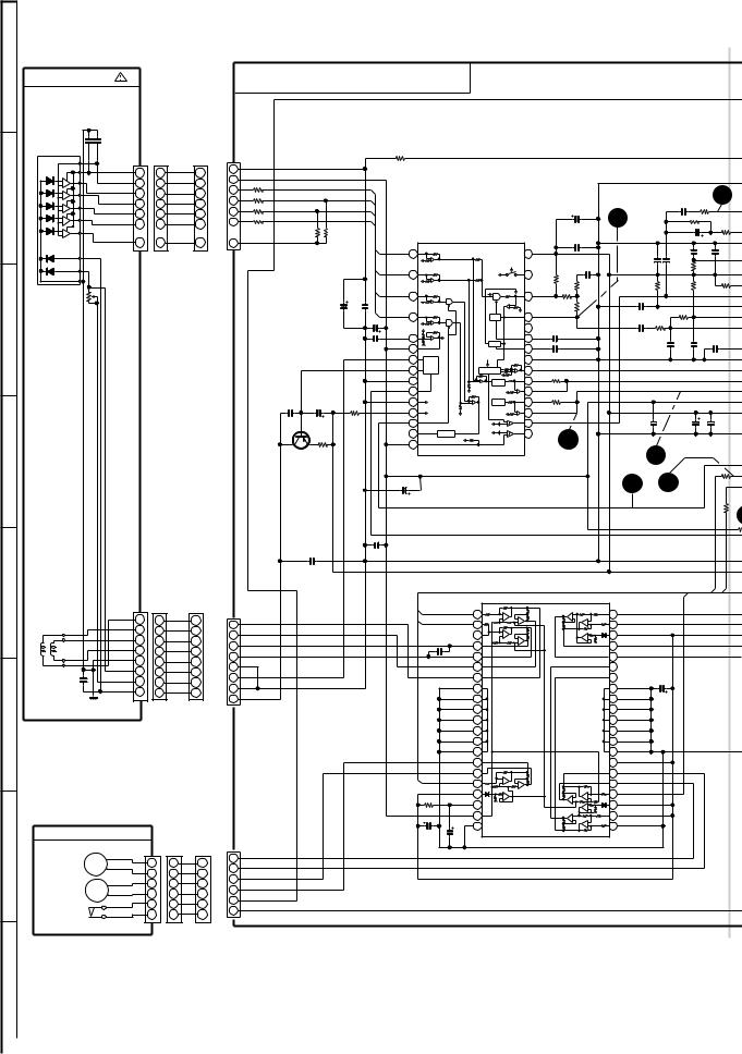
CD-BK310V
A |
PICKUP UNIT |
|
|
VCC |
7 |
|
VREF |
6 |
B |
E |
5 |
A |
4 |
|
|
B |
3 |
|
F |
2 |
|
C |
1 |
C
D
E
|
TR– |
1 |
|
TR+ |
TR+ |
2 |
|
FO+ |
FO+ |
3 |
|
FO– |
4 |
||
FO– |
|
5 |
|
TR– |
PD |
||
6 |
|||
|
VR |
7 |
|
|
LD |
8 |
GND
F
|
CD MOTOR PWB-F |
||
G |
M1 |
+ |
|
SPINDLE |
|||
M – |
|||
|
MOTOR |
||
|
M2 |
+ |
|
|
SLED |
||
|
M – |
||
|
MOTOR |
||
|
SW4 |
|
|
|
PICKUP IN |
|
|
H
|
|
|
|
VIDEO CD PWB-B(1/2) |
|
|
|
|
|
|
|
|
|
|
|
|
|
|
|
|||||||
|
|
|
|
|
|
|
|
|
|
|
|
|
|
|
|
|
|
|
|
|
|
|
|
|
|
IC |
|
|
|
|
|
|
|
|
|
|
|
|
|
|
|
|
|
|
|
|
|
|
|
|
LC78 |
||
|
CNS1B |
CNS1A |
|
|
|
|
|
|
R50 |
|
|
|
|
|
|
|
|
|
|
|
|
|
|
SERVO/ |
||
|
|
|
|
|
|
|
|
|
|
|
|
|
|
|
|
|
|
|
|
|
CON |
|||||
|
|
|
|
CNP9 |
|
|
|
|
47 |
|
+B |
|
|
|
|
|
|
|
|
|
|
|
|
|||
|
7 |
7 |
7 |
|
|
|
|
|
|
|
|
|
|
|
|
|
|
|
|
|
|
|
|
|
|
|
|
6 |
|
|
|
|
|
|
|
|
|
|
|
|
|
|
|
|
|
|
|
|
|
|
|
||
|
6 |
6 |
R51 68K |
|
|
|
TIN1 |
|
|
|
|
|
|
|
|
|
|
|
|
|
|
|
|
|
|
|
|
5 |
|
|
|
|
|
|
|
|
|
|
|
|
|
|
|
|
|
|
|
7 |
|||||
|
5 |
5 |
R52 56K |
|
|
|
FIN1 |
|
|
|
|
|
|
|
|
|
|
|
|
|
|
C23 |
R12 |
|||
|
4 |
|
|
|
|
|
|
|
|
|
|
|
|
|
|
|
|
|
||||||||
|
|
|
|
|
|
|
|
|
|
|
|
|
|
|
C11 |
|
|
|
||||||||
|
4 |
4 |
3 |
R53 56K |
|
|
|
FIN2 |
|
|
|
|
|
|
|
|
|
|
|
|
0.047 |
680 |
|
PD |
||
|
3 |
3 |
R54 68K |
|
|
|
TIN2 |
|
|
|
|
|
|
|
|
|
47/6.3 |
5 |
|
R79 |
1.5M |
R13 |
||||
|
2 |
|
|
|
|
|
|
|
|
|
|
|
|
|
|
|
||||||||||
|
2 |
2 |
|
|
|
|
|
|
|
|
|
|
|
|
|
|
|
|||||||||
|
R56 |
R55 |
|
|
|
|
|
|
|
|
|
|
C12 |
|
C24 |
|
680 PD0 |
|||||||||
|
|
|
|
|
|
|
|
|
|
|
|
|
|
|
|
|
|
|||||||||
|
|
|
|
56K |
56K |
|
|
|
|
|
|
|
|
|
|
|
|
|
2.2/50 |
|
VVS |
|||||
|
1 |
1 |
1 |
|
|
|
|
|
|
|
|
|
|
0.022 |
|
|
|
|
||||||||
|
|
|
|
|
|
|
|
|
|
|
|
|
|
|
|
|
|
|
C21 |
|
||||||
|
|
|
|
|
|
FIN1 |
|
|
|
|
|
|
|
VCC |
|
|
|
|
|
|
C81 0.0 |
|||||
|
|
|
|
|
|
|
|
|
1 |
|
|
|
|
|
30 |
|
|
|
|
|
C22 |
|||||
|
|
|
|
|
|
|
|
|
|
|
|
|
|
|
|
|
C18 |
|
C25 |
|
0.1 |
PCKIS |
||||
|
|
|
|
|
|
|
|
|
|
|
REF |
|
|
ODRV |
RFSW |
|
|
0.022 |
100P |
R11 |
|
|
||||
|
|
|
|
|
|
|
|
|
FIN2 2 |
|
|
6P(CH) |
|
(CH) |
|
VVD |
||||||||||
|
|
|
|
|
|
|
|
|
|
|
REF |
|
|
29 |
R42 |
|
|
|
|
|
|
12K |
|
|||
|
|
|
|
|
|
|
|
|
|
|
REF |
|
AGCON |
|
|
56K |
R5 |
R7 |
|
R10 |
R80 |
R14 |
|
F |
||
|
|
|
|
|
|
|
|
C55 0.01 |
TIN1 |
|
|
|
|
RF– |
39K |
|
27K |
1M |
1.2K |
|
HF |
|||||
|
|
|
|
|
|
C54 47/10 |
3 |
|
|
|
REF |
28 |
6.8K |
|
|
|||||||||||
|
|
|
|
|
|
TIN2 |
|
|
|
RF |
27K |
|
|
C20 |
R8 |
10K |
|
|
SLC |
|||||||
|
|
|
|
|
|
|
|
|
|
|
REF |
|
|
|
|
|
|
R6 |
|
|
|
|
R15 |
|
SLCIS |
|
|
|
|
|
|
|
|
|
|
|
|
|
|
|
|
|
|
|
|
|
|
|
|
|
|
|
|
|
|
|
|
|
|
|
|
|
|
4 |
|
|
PH |
|
|
27 |
|
C13 |
|
|
0.1 |
330 |
|
|
|
EFMI |
|
|
|
|
|
|
|
|
|
|
|
REF |
|
|
|
|
26 |
|
|
|
|
|
|
|
|||
|
|
|
|
|
|
C6 100/6.1 |
REF1 |
|
|
|
|
|
PH |
|
|
C17 |
|
|
C27 |
JITT |
||||||
|
|
|
|
|
|
|
REF |
|
|
|
|
|
0.01 |
|
|
68P |
C26 0.047 |
|||||||||
|
|
|
|
|
|
|
|
C8 |
VREF 6 |
|
|
|
|
24 BH |
|
|
|
|
|
|
JITT |
|||||
|
|
|
|
|
|
|
|
|
|
5 |
|
|
DH |
|
|
25 |
|
C14 |
|
|
0.0047 |
C42 |
|
0.1 |
|
|
|
|
|
|
|
|
|
|
0.1 |
|
7 |
|
ODRV |
|
|
23 |
|
0.33 |
|
|
|
(CH) |
|
|
|
B |
|
|
|
|
|
|
|
|
|
|
|
|
|
|
|
|
|
|
|
|
|
|
|
|||||
|
|
|
|
|
|
|
|
|
LDD |
APC |
PH/BH |
|
|
|
|
|
|
|
|
|
PH(RFENV |
|||||
|
|
|
|
|
|
|
|
|
8 |
|
|
22 RFEV |
|
|
|
|
|
|
||||||||
|
|
|
|
|
|
|
|
|
|
|
|
|
|
|
|
|
|
|
|
|
|
|
|
|
|
|
|
|
|
|
|
|
|
|
|
GND |
9 |
|
|
REF |
|
21 |
FE– R3 47K |
|
|
|
|
|
|
F |
|||
|
|
|
|
|
|
|
|
|
LDON |
|
REF |
LPF |
|
FE |
|
|
|
|
|
|
|
|
T |
|||
|
|
|
|
|
|
C51 |
|
|
10 |
|
REF |
|
20 |
R4 |
|
|
|
|
|
|
|
|||||
|
|
|
|
C53 |
|
|
|
|
|
|
|
TE– |
|
|
|
|
|
|
|
VRE |
||||||
|
|
|
|
|
|
|
|
11 |
ODRV |
|
LPF |
|
19 |
|
|
|
|
|
|
|
||||||
|
|
|
|
0.001 |
|
47/6.3 |
|
|
|
|
|
TE |
10K |
|
|
|
|
|
|
ADAVD |
||||||
|
|
|
|
|
|
|
|
|
AGON 12 |
AGCON |
|
REF |
|
18 |
|
|
|
|
|
|
|
|||||
|
|
|
|
3.2 V |
|
|
R25 |
EFBL |
13 |
REF |
REF |
|
|
17 |
HFL |
|
|
|
C82 |
|
C28 |
|
|
|
||
|
|
|
|
R47 |
|
10K |
|
|
|
|
|
|
|
|
0.022 |
|
47/10 |
|
ADAVS |
|||||||
|
|
|
|
|
|
|
|
TEST0 14 |
LPF |
REF |
|
|
16 TEST |
4 |
|
|
|
|
|
|
||||||
|
|
|
|
|
|
3.3 |
|
|
TES1 15 |
REF |
|
|
|
|
|
|
|
|
|
|
|
C29 PHRE |
||||
|
|
|
|
1.6 V |
|
8.4 V |
|
|
|
|
|
|
|
|
|
|
|
|
|
|
|
4 |
|
0.022 BHRE |
||
|
|
|
|
|
Q3 |
|
|
|
|
|
|
|
|
|
|
|
|
|
|
|
|
|
|
TBL |
||
|
|
|
|
KTA1504 GR |
|
|
|
|
|
IC1 |
|
|
|
|
|
|
|
|
|
|
EFBL 1K |
|
TD |
|||
|
|
|
|
DRIVER |
|
|
|
|
|
|
|
|
|
|
|
|
|
|
|
|
||||||
|
|
|
|
|
|
|
|
|
|
|
|
|
|
|
|
|
|
|
|
|
|
FD |
||||
|
|
|
|
LASER |
|
|
|
|
LA9235M |
|
|
|
|
|
|
13 |
2 |
|
|
|
||||||
|
|
|
|
|
|
|
|
|
|
|
|
|
|
|
|
|
R44 |
|
|
|||||||
|
|
|
|
|
|
|
|
|
1000/6C88 .3 SERVO AMP. |
|
|
|
|
|
|
|
|
|
R35 |
|||||||
|
|
|
|
|
|
|
|
|
|
|
|
|
|
|
|
|
|
|
|
|
|
|
|
|
|
1K |
|
|
|
|
|
|
|
|
|
C19 |
|
|
|
|
|
|
|
|
|
|
|
|
|
|
|
|
R |
|
|
|
|
|
|
C52 |
|
|
|
|
|
|
|
|
|
|
|
|
|
|
|
|
|
|
1. |
|
|
|
|
|
|
|
|
|
0.022 |
|
|
|
|
|
|
|
|
|
|
|
|
|
|
|
|||
|
|
|
|
|
|
0.01 |
|
|
|
|
|
|
|
|
|
|
|
|
|
|
|
|
|
|
||
|
|
|
|
|
|
|
|
|
|
|
|
|
|
|
|
|
|
|
|
|
|
|
|
|
|
|
|
CNS2B |
CNS2A |
|
CNP10 |
|
|
|
|
|
|
TDO |
1 |
|
– |
|
|
|
+ |
|
42 |
|
|
|
|
|
|
|
|
|
|
|
|
|
|
|
|
|
|
|
|
|
|
|
|
|
|
|
||||||
|
1 |
1 |
|
TR– |
|
|
|
|
|
|
FDO |
|
|
+ |
– |
|
|
– |
+ |
|
|
|
|
|
|
|
|
1 |
|
|
|
|
|
|
2 |
|
|
+ |
|
|
|
41 |
|
|
|
|
|
|
|||||
|
2 |
2 |
TR+ |
|
|
|
|
|
|
|
|
|
|
|
|
|
– |
+B |
|
|
|
|
|
|||
|
2 |
|
|
|
|
|
|
C46 |
3 |
|
– |
|
|
|
|
+ |
40 |
|
|
|
|
|
||||
|
|
|
|
|
|
|
|
|
|
|
+ |
– |
|
|
|
|
|
|
|
|
|
|||||
|
3 |
3 |
|
FO+ |
|
|
|
|
|
|
0.022 |
|
|
|
|
|
|
– |
|
|
|
|
|
|
|
|
|
3 |
|
|
|
|
|
|
4 |
|
|
+ |
|
|
|
|
39 |
|
|
|
|
|
|
||||
|
4 |
4 |
FO– |
|
|
|
|
|
|
|
|
|
|
|
|
|
|
|
|
|
|
|
|
|||
|
4 |
|
|
|
|
|
|
|
5 |
|
|
|
|
|
|
|
38 |
|
|
|
|
|
|
|||
|
5 |
5 |
GND |
|
|
|
|
|
|
|
|
|
|
|
|
|
|
|
|
|
|
|
|
|||
|
5 |
|
|
|
|
|
|
|
6 |
|
|
|
|
|
|
|
37 |
|
|
|
|
|
|
|||
|
6 |
6 |
PD |
|
|
|
|
|
|
|
|
|
|
|
|
|
|
|
C47 |
|
|
|
|
|||
|
6 |
|
|
|
|
|
|
|
7 |
|
|
|
|
|
|
|
36 |
|
|
|
|
|
||||
|
7 |
7 |
VR |
|
|
|
|
|
|
|
|
|
M63001FP |
|
|
|
100/6.3 |
|
|
|
||||||
|
7 |
|
|
|
|
|
|
|
13 |
|
IC3 |
|
|
|
30 |
|
|
|
||||||||
|
8 |
8 |
LD |
|
|
|
|
|
|
|
8 |
|
|
|
|
|
|
|
35 |
|
|
|
|
|
|
|
|
8 |
|
|
|
|
|
|
|
9 |
|
|
|
|
|
|
|
34 |
|
|
|
|
|
|
|||
|
|
|
|
|
|
|
|
|
|
|
|
|
|
|
|
|
|
|
|
|
|
|
|
|||
|
|
|
|
|
|
|
|
|
|
|
|
10 |
|
|
|
|
|
|
|
33 |
|
|
|
|
|
|
|
|
|
|
|
|
|
|
|
|
|
|
11 |
|
|
|
|
|
|
|
32 |
|
|
|
|
|
|
|
|
|
|
|
|
|
|
|
|
|
|
12 |
|
|
|
|
|
|
|
31 |
|
+B |
|
|
|
|
|
|
|
|
|
|
|
|
|
|
|
|
|
|
|
|
|
|
|
|
|
|
|
|
|
||
|
|
|
|
|
|
|
|
|
|
|
|
14 |
|
|
|
|
|
|
|
29 |
+B |
|
|
|
|
|
|
|
|
|
|
|
|
|
|
|
|
|
15 |
|
|
|
|
|
|
|
28 |
|
|
|
|
|
|
|
|
|
|
|
|
|
|
|
|
|
|
|
|
|
|
|
|
|
|
|
|
|
|
|
||
|
|
|
|
|
|
|
|
|
|
|
|
16 |
|
– |
|
|
|
|
|
27 |
|
|
|
|
|
|
|
|
|
|
|
|
|
|
|
|
|
|
|
|
– |
|
|
|
|
|
|
|
|
|
|
|
|
|
|
|
|
|
|
|
|
|
|
|
|
17 |
|
+ |
|
|
|
|
26 |
|
|
|
|
|
|
|
|
|
|
|
|
|
|
|
|
|
|
+B |
|
|
+ |
|
|
|
|
|
|
|
|
|
|
||
|
|
|
|
|
|
|
|
|
|
|
18 |
|
+ |
|
|
|
– |
– |
25 |
|
|
|
|
|
|
|
|
|
|
|
|
|
|
|
|
R48 |
|
|
|
– |
|
|
|
+ |
|
+B |
|
|
|
|
|
||
|
|
|
|
|
|
|
|
|
|
19 |
|
|
|
|
|
+ |
+ |
24 |
|
|
|
|
|
|||
|
|
|
|
|
|
|
|
|
6.8K |
|
20 |
|
|
|
|
|
|
– |
23 |
+B |
|
|
|
|
|
|
|
|
|
|
|
|
|
|
|
|
|
|
|
|
|
|
|
+ |
|
|
|
|
|
|
|||
|
|
|
|
|
|
|
|
|
C50 |
|
21 |
|
|
|
|
|
– |
+ |
22 |
|
|
|
|
|
|
|
|
CNS3B |
CNS3A |
|
|
|
|
|
|
100/10 |
|
|
|
|
|
|
|
– |
|
|
|
|
|
|
|||
|
|
|
|
|
|
|
|
|
|
|
|
|
|
|
|
|
|
|
|
|
|
|
||||
|
|
|
|
CNP3 |
|
|
|
|
|
|
|
|
|
|
|
|
|
|
|
|
|
|
|
|
|
|
|
|
|
6 |
SP+ |
|
|
|
|
|
|
C49 100/10 |
|
|
|
|
|
|
|
|
|
|
|
|
|
|
|
6 |
6 |
6 |
SP– |
|
|
|
|
|
|
|
|
|
|
|
|
|
|
|
|
|
|
|
|
|
|
|
5 |
|
|
|
|
|
|
|
|
|
|
|
|
|
|
|
|
|
|
|
|
|
|
||||
5 |
5 |
5 |
SL+ |
|
|
|
|
|
|
|
|
|
|
|
|
|
|
|
+B |
|
|
|
|
|
|
|
4 |
|
|
|
|
|
|
|
|
|
|
|
|
|
|
|
|
|
|
|
|
|
|||||
4 |
4 |
4 |
SL– |
|
|
|
|
|
|
|
|
|
|
IC3 |
|
|
|
|
|
|
|
|
|
|||
3 |
|
|
|
|
|
|
|
|
|
|
|
|
|
|
|
|
|
|
|
|||||||
3 |
|
|
|
|
|
|
|
|
|
|
|
|
|
|
|
|
|
|
|
|||||||
3 |
3 |
2 |
PUIN |
|
|
|
|
|
|
|
|
M63001FP |
|
|
|
|
|
|
|
|
||||||
2 |
2 |
2 |
GND(D) |
|
|
|
|
|
|
|
|
|
|
|
|
|
|
|
|
|||||||
1 |
|
|
|
|
|
|
|
|
|
|
|
|
|
|
|
|
||||||||||
1 |
1 |
1 |
|
|
|
|
|
FOCUS/TRACKING/SPIN/SLED DRIVER |
|
|
|
|
||||||||||||||
|
|
|
|
|
|
|
|
|
|
|||||||||||||||||
|
|
|
|
|
|
|
|
|
|
|
|
|
||||||||||||||
• NOTES ON SCHEMATIC DIAGRAM can be found on page 18.
|
1 |
2 |
3 |
4 |
5 |
6 |
Figure 22 SCHEMATIC DIAGRAM (1/12)
– 22 –
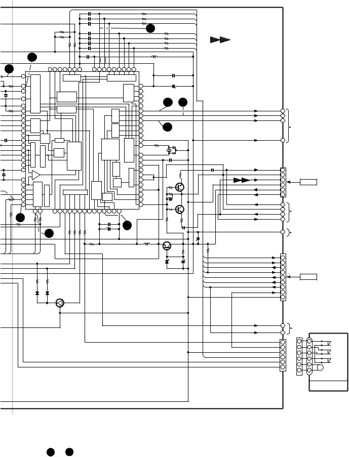
|
|
|
|
|
|
|
|
|
|
|
|
|
|
|
|
|
|
|
|
|
|
|
|
|
|
|
|
|
|
|
|
|
|
|
|
|
|
|
CD-BK310V |
|||
|
|
|
|
|
|
OPENNMP3O |
|
|
C71 |
100P(CH) |
|
|
R71 |
|
1K |
|
|
|
|
|
|
|
|
|
|
|
|
|
|
|
|
|
|
|
|
|||||||
|
|
|
|
|
|
|
|
C72 |
0.01 |
|
|
|
|
R72 |
|
1K |
|
|
|
|
|
|
|
|
|
|
|
|
|
|
|
|
|
|
|
|
||||||
|
|
|
|
|
|
|
DISC-NO |
|
|
C73 |
100P |
|
|
|
|
R73 |
|
1K |
|
|
|
|
|
|
|
|
|
|
|
|
|
|
|
|
|
|
|
|
||||
|
|
|
|
|
|
|
|
|
|
|
|
|
|
|
|
|
|
|
|
|
|
|
|
|
|
|
|
|
|
|
|
|
|
|
|
|
|
|||||
|
|
IC2 |
|
|
|
|
|
|
R94 |
|
|
(CH) |
|
|
|
|
|
|
|
|
3 |
|
|
|
|
|
|
|
|
|
|
|
|
|
|
|
|
|
|
|
|
|
|
|
|
|
|
|
|
|
10K |
|
|
C75 |
|
|
C75~C78 |
100P(CH) |
|
R75 |
|
100 |
|
|
|
|
|
|
|
|
|
|
|
|
|
||||||||||
|
|
|
|
|
|
|
|
|
|
|
|
|
|
|
|
|
|
|
|
|
|
|
|
|
|
|
|
|||||||||||||||
LC78636E |
R95 |
|
|
|
R67 |
1K |
C76 |
|
|
|
|
|
|
|
|
|
|
R76 |
|
1K |
|
|
|
|
|
CD SIGNAL |
|
|
|
|
|
|||||||||||
ERVO/SIGNAL |
10K |
|
|
R68 |
C77 |
|
|
|
|
|
|
|
|
|
|
R77 |
|
1K |
|
|
|
|
|
|
|
|
|
|
||||||||||||||
CONTROL |
|
+B |
|
1K |
|
|
C78 |
|
|
|
|
|
|
|
|
|
|
R78 |
|
1K |
|
|
|
|
|
|
|
|
|
|
|
|
|
|||||||||
|
|
V/P CONT7 |
CONT6 |
|
|
|
|
|
|
|
|
|
|
|
|
2.2 H |
|
+B |
|
|
|
|
|
|
|
|
|
|
|
|
||||||||||||
|
|
|
|
8 |
|
|
DEFECT |
FSEQ |
VSS |
C80 |
0.1 |
RES |
WRQ |
|
|
|
|
|
L62 |
|
|
|
|
|
|
|
|
|
|
|
|
|
|
|
|
|||||||
|
|
|
|
|
|
|
DEF |
DO DI |
CL |
CE |
|
|
|
|
|
|
|
|
|
|
|
|
|
|
|
|
|
|
|
|
|
|
|
|||||||||
|
|
|
|
|
|
|
|
|
|
|
|
|
|
|
|
|
|
|
|
|
|
|
|
|
|
|
|
|
|
|
|
|||||||||||
|
7 |
|
|
|
|
|
|
|
|
|
|
VDD5V |
|
|
|
|
|
|
|
|
|
|
|
|
|
|
|
|
|
|
|
|
|
|
|
|
|
|
|
|
||
12 |
|
|
EFMO 80 79 78 77 76 75 74 |
73 72 71 70 69 68 67 66 65 |
|
|
|
|
|
|
|
C44 |
0.022 |
|
|
|
|
|
|
|
|
|
|
|
||||||||||||||||||
80 |
|
PD01 1 |
|
|
|
|
|
|
|
|
|
|
|
|
COMMAND |
|
|
|
|
|
|
|
|
|
|
|
|
|
|
|
|
|
|
|||||||||
|
|
|
|
|
|
|
|
GENERAL |
|
|
|
|
|
|
|
|
|
|
|
|
|
|
|
|
|
|
|
|
|
|
|
|
|
|||||||||
5M R13 |
|
|
|
|
|
|
|
|
|
INTERFACE |
|
|
|
|
|
|
|
|
|
|
|
|
|
|
|
|
|
|
|
|
|
|
|
|||||||||
|
|
|
|
|
|
|
|
|
|
|
|
|
|
|
|
|
|
|
|
|
|
|
|
|
|
|
|
|
|
|
|
|
|
|
|
|||||||
|
680 PD02 |
2 |
|
|
|
|
|
|
|
|
|
|
IC2 |
|
SUBCODE DECODE CRC |
64 |
SBCK |
|
|
|
|
C45 |
100/10 |
|
|
|
|
|
|
|
|
|
|
|
||||||||
|
|
VVSS |
|
PLL VCEC |
|
|
|
|
|
|
|
|
|
PW |
|
|
|
|
|
|
|
|
|
|
|
|
|
|
|
|
|
|
|
|
||||||||
|
|
3 |
|
|
|
|
|
|
|
|
|
|
63 |
|
|
|
|
|
|
|
|
|
|
|
|
|
|
|
|
|
|
|
|
|||||||||
21 |
C81 0.022 |
|
|
|
|
|
FRAME SYNC |
|
|
LC78636E |
SBSY |
|
|
|
|
|
|
|
|
|
|
|
|
|
|
|
|
|
|
|
|
|||||||||||
.1 |
PCKIST |
4 |
|
|
|
|
DEFECT,PROTECT |
|
|
|
|
|
62 |
SFSY |
|
|
|
|
12 |
11 |
|
|
|
|
|
|
|
|
|
|
|
|||||||||||
11 |
|
|
|
|
|
|
|
EFM DECODE |
|
|
|
|
|
|
61 |
|
|
|
|
|
|
|
|
|
|
|
|
|
|
|
||||||||||||
K |
|
VVDD 5 |
|
|
|
|
|
|
CLV |
|
|
|
|
|
|
|
|
|
60 |
16M |
|
|
|
|
|
|
|
|
|
|
|
|
|
|
|
|||||||
14 |
|
FR |
6 |
|
|
|
|
|
|
|
|
|
|
|
EXTERNAL SERIAL AUDIO IN OUT |
|
|
|
DATA |
|
|
|
|
|
|
|
|
|
|
|
|
|
|
DATA |
1 |
|
|
|
|
|||
|
|
|
|
|
|
CONTROL |
|
|
|
|
|
59 |
|
|
|
|
|
|
|
|
|
|
|
|
|
|
|
|
|
|
||||||||||||
.2K |
|
HFL 7 |
|
|
|
|
|
|
|
|
|
|
|
|
|
|
|
DATACK |
|
|
|
|
|
|
|
|
|
|
|
DATACK |
2 |
MP3 SECTION P24 1-E |
|
|
|
|||||||
|
|
|
|
|
|
|
|
|
|
|
|
|
|
|
|
58 |
|
|
|
|
|
|
|
|
|
|
|
|
|
|
||||||||||||
|
SLCIST |
8 |
SLICE LEVEL CONTROL |
|
|
|
|
|
|
|
|
|
|
|
|
57 |
LRSY |
|
|
|
|
|
|
|
|
|
|
|
|
|
|
LRSY |
3 |
|
|
|
||||||
|
|
SLCO |
9 |
|
|
|
|
|
|
|
|
|
|
|
|
56 |
ASDFIN |
|
|
10 |
|
|
|
|
|
|
|
|
|
|
|
|
||||||||||
|
|
EFMIN |
|
|
|
|
|
|
|
|
|
|
|
|
ASDACK |
|
|
|
+B |
|
|
|
|
|
|
|
|
|
||||||||||||||
|
|
10 |
|
|
|
|
|
|
|
|
|
|
|
|
55 |
|
|
|
|
|
|
|
|
|
|
|
|
|||||||||||||||
|
|
|
|
|
|
|
|
|
|
|
|
|
|
|
|
|
|
|
|
|
|
|
|
|
|
|
||||||||||||||||
C27 |
JITTV |
11 |
JITER |
|
|
|
|
|
|
|
|
|
|
|
54 ASLRCK |
|
|
XL2 |
|
|
|
|
|
|
+B |
+5V |
|
|
|
|
||||||||||||
0.1 |
JITTC |
12 |
|
|
DEFECT |
|
|
SW |
|
|
|
|
|
|
|
CLOCK GENERATOR |
53 |
XVSS |
|
|
|
|
|
|
|
|
|
|
4 |
TO |
|
|
|
|||||||||
|
|
BH |
|
CONTROL |
|
|
|
|
|
|
ATTENUATION |
DEEMPHASIS |
|
|
|
|
16.9344MHz C85 |
|
|
|
|
|
|
|
|
|
||||||||||||||||
|
|
|
|
|
|
|
|
|
|
|
|
|
|
|
|
|
|
|
|
|
|
|
|
|
|
|
||||||||||||||||
|
|
13 |
|
|
|
|
|
|
|
|
|
|
|
|
52 |
|
|
|
|
|
|
|
|
|
|
|
|
|
|
|||||||||||||
PH(RFENV) |
14 |
|
|
|
|
|
AUTO |
|
|
|
|
|
|
XOUT R20 |
|
|
|
|
8P(CH) |
|
|
|
|
|
|
|
|
|
|
|||||||||||||
|
|
FE |
|
SW |
|
|
|
|
|
|
|
|
|
XIN |
220 |
|
|
|
|
C86 |
|
|
|
|
|
|
|
|
|
|
||||||||||||
|
|
15 |
|
|
|
ADJUST |
|
|
|
|
|
51 |
|
|
|
|
|
|
|
|
|
|
|
|
|
|
|
|
|
|||||||||||||
|
|
TE |
|
|
|
|
|
|
|
|
XVDD |
|
+B |
|
|
|
10P(CH) |
|
|
|
|
|
|
|
|
|
|
|||||||||||||||
|
|
|
|
|
|
|
|
|
|
|
|
|
|
|
|
|
|
|
|
C84 |
|
|
|
|
|
|
||||||||||||||||
|
|
16 |
|
|
A/D |
|
|
|
|
SERVO |
PROCESSEROR |
|
|
|
INTERPOLATION MUTE DIGITAL FILTER |
50 |
|
|
|
|
|
|
|
|
|
|
|
|
|
|
|
|
|
|||||||||
|
|
|
|
|
|
|
|
|
|
|
|
|
|
|
|
|
|
|
|
C34 0.022 |
|
|
|
0.047 |
|
|
|
|
|
|
|
|||||||||||
|
|
VREF |
17 |
|
|
|
|
|
|
|
|
|
49 RVDD +B |
|
|
|
|
|
|
|
|
CNP11 |
|
|
|
|||||||||||||||||
|
|
|
|
|
|
|
|
|
|
|
|
|
|
|
|
|
|
|
|
|
R-CH |
|
|
|
|
|||||||||||||||||
|
ADAVDD |
18 |
|
|
|
|
|
|
|
|
|
48 |
RCHO |
|
|
|
|
|
|
|
|
|
|
|
|
|
1 |
FROM |
|
|
||||||||||||
|
|
|
|
+ |
|
|
|
|
|
|
|
RVSS |
|
|
|
|
|
R117A |
|
|
|
|
|
AGND |
|
|
|
|||||||||||||||
|
|
|
|
|
|
|
|
|
|
|
|
47 |
|
|
|
|
|
|
GR |
|
|
|
|
2 |
MAIN PWB |
|
||||||||||||||||
|
|
|
|
|
– |
|
|
|
|
|
|
|
|
|
|
|
|
|
|
|
330 |
|
|
|
|
|
|
|
P26 1-A |
|
||||||||||||
|
ADAVSS |
|
|
|
|
|
|
|
|
|
|
|
|
|
|
|
LPF |
LVSS |
|
|
|
|
|
|
|
|
|
|
|
L-CH |
|
|
||||||||||
|
19 |
|
|
|
|
|
|
|
|
|
|
|
|
|
1BIT DAC |
|
46 |
|
|
|
|
R118A |
|
0 V |
|
|
|
|
3 |
|
|
|
|
|||||||||
C29 PHREF 20 |
|
|
|
|
|
|
|
|
|
|
|
|
|
|
|
LCHO |
|
|
|
|
|
|
|
|
DGND |
|
|
CNS11 |
|
|||||||||||||
|
|
|
|
|
|
|
|
|
|
|
|
|
|
45 |
|
|
|
|
|
2.2K |
|
|
|
|
+B |
|
4 |
|
||||||||||||||
.022 BHREF |
21 |
|
|
|
|
|
|
|
|
|
|
ERROR CORRECT |
|
|
|
|
|
44 |
LVDD |
|
|
R114A |
|
0.6 V |
|
Q10 |
KTC3875 |
|
|
+5V |
|
5 |
|
|
|
|
||||||
|
|
|
|
|
|
|
|
|
GENERAL |
|
|
|
|
|
MUTER |
|
22K |
|
|
|
|
A10V |
|
|
|
|
|
|||||||||||||||
|
|
TBLO 22 |
|
S/H |
D/A |
FG(DVref) |
|
AUDIO |
|
|
|
43 |
|
|
|
|
|
|
+B |
|
6 |
|
|
|
|
|||||||||||||||||
|
|
TDO 23 |
|
|
LASER |
CONT1 CONT2 |
CONT3 |
CONT4 |
CONT5 |
|
|
|
|
MUTEL |
|
|
CE1 0 V |
|
|
|
|
|
|
|
|
|
|
|||||||||||||||
1K |
|
|
|
|
OUT |
EFLG |
|
|
42 |
|
|
|
|
|
|
|
|
|
|
|
|
|||||||||||||||||||||
|
FDO |
24 |
|
|
|
FSX |
|
|
41 |
|
|
|
|
|
1/50 |
0 V |
|
|
|
R-CH |
5 |
|
|
|
|
|||||||||||||||||
|
|
|
|
|
EMPH |
|
|
|
|
1.1 V |
|
|
|
|
A_GND |
TO MP3 |
|
|
|
|||||||||||||||||||||||
R44 |
|
R35 |
SPDO 25 26 SLDO 27 28 29 30 31 32 33 34 35 36 37 38 39 40 TEST |
|
|
|
+B |
R113A |
2.2K |
|
|
|
|
KTC3875GR |
|
|
|
|
|
6 |
|
|
|
|||||||||||||||||||
|
|
|
|
|
|
|
Q9 |
|
|
|
L-CH |
SECTION |
|
|
||||||||||||||||||||||||||||
|
1K |
|
|
|
|
|
|
|
|
|
|
|
7 |
|
|
|||||||||||||||||||||||||||
|
|
|
|
|
|
|
|
|
|
|
|
|
|
|
|
|
|
|
|
|
|
|
|
|
0 V |
|
|
|
|
|
P25 12-B |
|
|
|
||||||||
|
1 |
R38 |
R39 |
|
|
|
R40 1.2K |
R45 1.2K |
|
R17 1K PCK |
C2F VDD |
DOUT |
C30 |
|
|
|
|
|
|
|
|
|
|
|
|
+B |
A10V |
|
|
|
|
|
||||||||||
|
|
|
|
R46 1K |
|
|
|
|
|
|
|
|
R112A |
|
|
8 |
|
|
|
|
||||||||||||||||||||||
|
270 |
470 |
|
|
|
0.022 |
|
|
|
+B |
|
|
|
|
|
|
|
|
|
|
|
|
|
|||||||||||||||||||
|
|
|
|
|
|
|
|
|
|
|
|
330 |
|
|
|
|
|
|
|
|
|
|||||||||||||||||||||
|
R37 |
|
|
|
|
|
|
+B |
|
|
9 |
|
|
|
|
|
R116A |
1.5K |
|
C83 |
|
|
|
D_GND |
|
TO MP3 |
|
|
|
|||||||||||||
|
|
|
|
|
|
|
|
|
|
|
|
|
|
|
|
|
|
|
9 |
|
|
|
||||||||||||||||||||
|
|
1.5K |
|
|
6 |
|
|
|
|
|
|
|
|
C31 |
|
|
|
|
|
|
|
|
|
Q4 |
|
0.047 |
|
|
|
|
|
|
|
SECTION |
|
|
||||||
|
|
|
|
|
|
|
|
|
|
|
|
|
|
|
|
|
|
|
|
|
|
|
|
|
|
|
|
|
|
|
|
|
|
P24 1-E |
|
|
|
|||||
|
|
|
|
|
|
|
|
|
|
|
|
|
|
100/10 |
|
|
|
|
|
|
|
|
KTC3203 Y |
|
|
|
|
|
|
|
|
|
|
|
||||||||
|
|
|
|
|
|
|
|
|
|
|
|
|
|
|
|
|
|
|
|
|
|
|
|
|
0 V |
|
+B |
|
|
|
|
+B |
|
|
|
|
|
|
|
|||
|
|
|
|
|
|
|
|
|
|
|
|
|
R16 |
|
|
|
|
|
|
L61 |
|
|
|
|
|
|
0 V |
|
|
|
|
1000/6.3 |
R97 |
|
|
|
|
|
|
|
||
|
|
|
|
|
|
|
|
|
|
|
|
|
10K |
|
|
|
|
|
0.82 H |
|
|
|
|
|
|
R58 |
|
|
C87 |
|
|
|
CNP12 |
|
|
|
||||||
|
|
|
|
|
|
|
|
|
|
|
|
|
|
|
|
|
|
|
|
|
|
|
|
|
|
3.9K |
|
|
|
|
|
|
||||||||||
|
|
|
|
|
|
|
|
|
|
|
|
|
|
|
|
|
|
|
|
|
|
|
|
|
|
Z02W3.9Z |
3.2 V |
68 |
|
|
WRQ |
|
|
|
|
|
|
|||||
|
|
|
|
|
|
|
|
|
|
|
|
|
|
|
|
|
|
|
|
|
|
|
|
|
|
|
|
|
|
|
|
|
1 |
|
|
|
|
|||||
|
|
|
|
|
|
|
|
|
|
|
|
|
|
|
|
|
|
|
|
|
|
|
|
|
ZD61 |
|
|
|
|
|
|
DRF |
|
|
|
|
|
|||||
|
|
|
|
|
|
|
|
|
|
|
|
|
|
|
|
|
|
|
|
|
|
|
|
|
|
C64 |
|
|
|
|
2 |
FROM |
|
|
||||||||
|
|
|
|
|
|
|
|
|
|
|
|
|
|
|
|
|
|
|
|
|
|
|
|
|
|
|
|
|
CE |
|
|
|
||||||||||
|
|
|
|
|
|
|
|
|
|
|
|
|
|
|
|
|
|
|
|
|
|
|
|
|
|
47/6.3 |
|
|
|
|
3 |
DISPLAY PWB |
|
|||||||||
|
|
|
|
|
|
|
|
|
|
|
|
|
|
|
|
|
|
|
|
|
|
|
|
|
|
|
|
|
DO |
|
|
|||||||||||
|
|
|
|
|
|
|
|
|
|
|
|
|
|
|
|
|
|
|
|
+B |
|
|
|
|
|
|
|
|
|
4 |
P29 10-B |
|
||||||||||
|
|
|
|
|
|
|
|
|
|
|
|
|
|
|
|
|
|
|
|
|
|
|
|
|
|
|
|
|
|
|
|
|
|
|
||||||||
|
|
|
|
|
|
|
|
|
|
|
|
|
|
|
|
|
|
|
|
|
|
|
|
|
|
|
|
|
|
|
|
|
|
|
|
DI |
|
|
|
|
|
|
|
|
|
|
|
|
|
|
|
|
|
|
|
|
|
|
|
|
|
|
|
Q4: CONSTANT VOLTAGE |
|
|
|
|
|
5 |
CNS703 |
|
|||||||||||||
|
|
|
|
R21 |
|
R22 |
|
|
|
|
|
|
|
|
|
|
|
|
|
|
|
CLK |
|
|
||||||||||||||||||
|
|
|
|
|
|
|
|
|
|
|
|
|
|
|
|
|
|
|
|
|
|
|
|
|
|
|
|
|
|
|
|
6 |
|
|
|
|
||||||
|
|
|
|
470 |
|
470 |
|
|
|
|
|
|
|
|
|
|
|
|
|
|
|
|
|
|
|
|
|
|
|
|
|
|
|
CD RES |
|
|
|
|
|
|||
|
|
|
|
|
KDS193 |
|
|
KDS193 |
|
|
|
|
|
|
|
|
|
|
|
|
|
|
|
|
|
|
|
|
|
|
|
|
|
|
|
|
7 |
|
|
|
|
|
|
|
|
|
D21 |
|
D22 |
|
|
|
|
|
|
|
|
|
|
|
|
|
|
|
|
|
|
|
|
|
|
|
|
|
|
|
CLAMP SW |
|
|
|
|
|
|||
|
|
|
|
|
|
|
|
|
|
|
|
|
|
|
|
|
|
|
|
|
|
|
|
|
|
|
|
|
|
|
|
|
8 |
|
|
|
|
|||||
|
|
|
|
|
|
|
|
|
|
|
|
|
|
|
|
|
|
|
|
|
|
|
|
|
|
|
|
|
|
|
|
GND |
|
|
|
|
|
|||||
|
|
|
|
|
|
|
|
|
|
|
|
|
|
|
|
|
|
|
|
|
|
|
|
|
|
|
|
|
|
|
|
|
9 |
|
|
|
|
|||||
|
|
|
|
|
|
3 0 V |
|
|
|
|
|
|
|
|
|
|
|
|
|
|
|
|
|
|
|
|
|
|
|
|
|
|
|
|
|
|
||||||
|
|
|
|
|
|
1.2 V |
|
|
|
|
|
|
|
|
|
|
|
|
|
|
|
|
|
|
|
|
|
|
|
|
|
|
|
|
|
|
|
|
||||
|
|
|
|
|
|
|
|
2 |
|
|
Q2 |
|
|
|
|
|
|
|
|
|
|
|
|
|
|
|
|
|
|
|
|
|
|
|
|
|
|
|
|
|
|
|
|
|
|
|
|
|
|
|
|
1 |
KRC102 S |
|
|
|
|
|
|
|
|
|
|
|
|
|
|
|
|
|
|
|
|
|
|
|
|
|
|
|
|
|
|||
|
|
|
|
|
|
|
|
0 V |
|
|
|
|
|
|
|
|
|
|
|
|
|
|
|
|
|
|
|
|
|
|
|
|
|
|
|
|
|
|
|
|
|
|
|
|
|
|
|
|
|
|
|
|
|
|
|
|
|
|
|
|
|
|
|
|
|
|
|
|
|
|
|
|
|
|
|
|
|
|
RAC/NTSC |
10 |
TO MP3 |
|
|
|
|
|
|
|
|
|
|
|
|
|
|
|
|
|
|
|
|
|
|
|
|
|
|
|
|
|
|
|
|
|
|
|
|
|
|
|
|
|
|
SECTION |
|
|
||
|
|
|
|
|
|
|
|
|
|
|
|
|
|
|
|
|
|
|
|
|
|
|
|
|
|
|
|
|
|
|
|
|
|
|
|
|
RES 11 |
P24 1-E |
|
|
|
|
|
|
|
|
|
|
|
|
|
|
|
|
|
|
|
|
|
|
|
|
|
|
|
|
|
|
|
|
|
|
|
|
|
|
|
|
|
BI4 |
|
|
|||
|
|
|
|
|
|
|
|
|
|
|
|
|
|
|
|
|
|
|
|
|
|
|
|
|
|
|
|
|
|
|
|
|
|
|
|
|
|
|
SW1 |
|||
|
|
|
|
|
|
|
|
|
|
|
|
|
|
|
|
|
|
|
|
|
|
|
|
|
|
|
|
|
|
|
|
|
|
|
|
|
|
|
|
|
||
|
|
|
|
|
|
|
|
|
|
|
|
|
|
|
|
|
|
|
|
|
|
|
|
|
|
|
|
|
|
|
|
|
|
|
|
OPEN/CLOSE |
1 |
1 |
1 |
OPEN/CLOSE |
||
|
|
|
|
|
|
|
|
|
|
|
|
|
|
|
|
|
|
|
|
|
|
|
|
|
|
|
|
|
|
|
|
|
|
|
|
CLAMP |
|
|
||||
|
|
|
|
|
|
|
|
|
|
|
|
|
|
|
|
|
|
|
|
|
|
|
|
|
|
|
|
|
|
|
|
|
|
|
|
2 |
2 |
2 |
|
|
||
|
|
|
|
|
|
|
|
|
|
|
|
|
|
|
|
|
|
|
|
|
|
|
|
|
|
|
|
|
|
|
|
|
|
|
|
GND(D) |
|
SW2 |
||||
|
|
|
|
|
|
|
|
|
|
|
|
|
|
|
|
|
|
|
|
|
|
|
|
|
|
|
|
|
|
|
|
|
|
|
|
3 |
3 |
3 |
|
|||
|
|
|
|
|
|
|
|
|
|
|
|
|
|
|
|
|
|
|
|
|
|
|
|
|
|
|
|
|
|
|
|
|
|
|
|
DISC-NO |
|
CLAMP |
||||
|
|
|
|
|
|
|
|
|
|
|
|
|
|
|
|
|
|
|
|
|
|
|
|
|
|
|
|
|
|
|
|
|
|
|
|
4 |
4 |
4 |
|
SW3 |
||
|
|
|
|
|
|
|
|
|
|
|
|
|
|
|
|
|
|
|
|
|
|
|
|
|
|
|
|
|
|
|
|
|
|
|
|
LD |
M+ |
|
||||
|
|
|
|
|
|
|
|
|
|
|
|
|
|
|
|
|
|
|
|
|
|
|
|
|
|
|
|
|
|
|
|
|
|
|
|
|
|
|||||
|
|
|
|
|
|
|
|
|
|
|
|
|
|
|
|
|
|
|
|
|
|
|
|
|
|
|
|
|
|
|
|
|
|
|
|
5 |
|
|
|
DISC |
||
|
|
|
|
|
|
|
|
|
|
|
|
|
|
|
|
|
|
|
|
|
|
|
|
|
|
|
|
|
|
|
|
|
|
|
|
|
|
5 |
5 |
|
||
|
|
|
|
|
|
|
|
|
|
|
|
|
|
|
|
|
|
|
|
|
|
|
|
|
|
|
|
|
|
|
|
|
|
|
|
LD |
M– |
6 |
+ M |
NUMBER |
||
|
|
|
|
|
|
|
|
|
|
|
|
|
|
|
|
|
|
|
|
|
|
|
|
|
|
|
|
|
|
|
|
|
|
|
|
6 |
6 |
|||||
|
|
|
|
|
|
|
|
|
|
|
|
|
|
|
|
|
|
|
|
|
|
|
|
|
|
|
|
|
|
|
|
|
|
|
|
|
CNP4 |
— |
M3 T/T |
|||
|
|
|
|
|
|
|
|
|
|
|
|
|
|
|
|
|
|
|
|
|
|
|
|
|
|
|
|
|
|
|
|
|
|
|
|
|
|
|
CD LOADING |
|||
|
|
|
|
|
|
|
|
|
|
|
|
|
|
|
|
|
|
|
|
|
|
|
|
|
|
|
|
|
|
|
|
|
|
|
|
|
|
|
CNS4 |
|
|
MOTOR |
|
|
|
|
|
|
|
|
|
|
|
|
|
|
|
|
|
|
|
|
|
|
|
|
|
|
|
|
|
|
|
|
|
|
|
|
|
|
|
|
|
CD LOADING |
|
|
|
|
|
|
|
|
|
|
|
|
|
|
|
|
|
|
|
|
|
|
|
|
|
|
|
|
|
|
|
|
|
|
|
|
|
|
|
|
|
MOTOR PWB-E |
||
• The numbers 1 to 13 are waveform numbers shown in page 44.
7 |
8 |
9 |
10 |
11 |
12 |
Figure 23 SCHEMATIC DIAGRAM (2/12)
– 23 –
 Loading...