


CD-C831W
SERVICE MANUAL
No. S5934CDC831W/
CD-C831W
CD-C831W mini component system consisting of CD-C831W (Main unit), CP-C831 (Front speaker) and GBOXS0025AWM1 (Surround speaker).
• In the interests of user-safety the set should be restored to its original condition and only parts identical to those specified be used.
CONTENTS |
|
|
Page |
SAFETY PRECAUTION FOR SERVICE MANUAL ........................................................................................................... |
2 |
VOLTAGE SELECTION ..................................................................................................................................................... |
2 |
SPECIFICATIONS .............................................................................................................................................................. |
3 |
NAMES OF PARTS ........................................................................................................................................................... |
4 |
OPERATION MANUAL ...................................................................................................................................................... |
6 |
DISASSEMBLY .................................................................................................................................................................. |
7 |
REMOVING AND REINSTALLING THE MAIN PARTS ..................................................................................................... |
9 |
ADJUSTMENT ................................................................................................................................................................. |
10 |
NOTES ON SCHEMATIC DIAGRAM .............................................................................................................................. |
12 |
BLOCK DIAGRAM ........................................................................................................................................................... |
13 |
SCHEMATIC DIAGRAM / WIRING SIDE OF P.W.BOARD .............................................................................................. |
16 |
VOLTAGE ........................................................................................................................................................................ |
32 |
WAVEFORMS OF CD CIRCUIT ...................................................................................................................................... |
33 |
TROUBLESHOOTING (CD SECTION) ........................................................................................................................... |
34 |
FUNCTION TABLE OF IC................................................................................................................................................ |
39 |
FL DISPLAY ...................................................................................................................................................................... |
46 |
PARTS GUIDE/EXPLODED VIEW |
|
This document has been published to be used
SHARP CORPORATION– 1 – |
for after sales service only. |
|
|
|
The contents are subject to change without notice. |
CD-C831W
SAFETY PRECAUTION FOR SERVICE MANUAL
WARNINGS
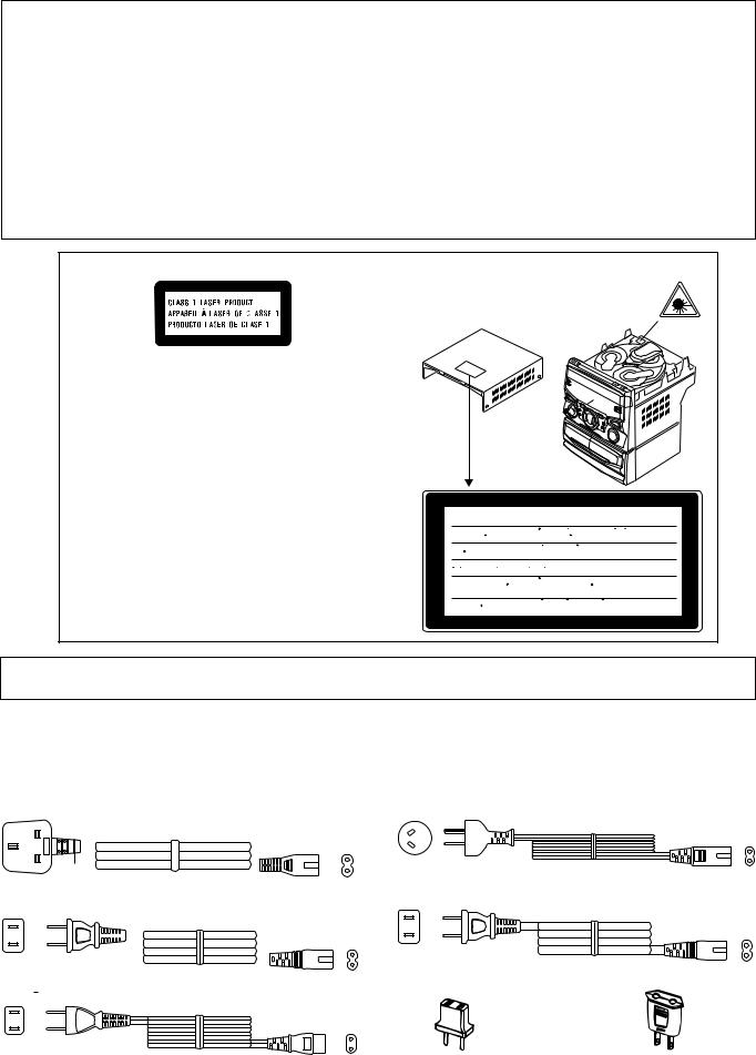
THE AEL (ACCESSIBLE EMISSION LEVEL) OF THE LASER POWER OUTPUT IS LESS THAN CLASS 1 BUT THE LASER COMPONENT IS CAPABLE OF EMITTING RADIATION EXCEEDING THE LIMIT FOR CLASS 1. THEREFORE IT IS IMPORTANT THAT THE FOLLOWING PRECAUTIONS ARE OBSERVED DURING SERVICING TO PROTECT YOUR EYES AGAINST EXPOSURE TO THE LASER BEAM.
1-WHEN THE CABINET IS REMOVED, THE POWER IS TURNED ON WITDOUT A COMPACT DISC IN POSITION AND THE PICK-UP IS ON THE OUTER EDGE THE LASER WILL LIGHT FOR SEVERAL SECONDS TO DETECT A DISC. DO NOT LOOK INTO THE PICK-UP LENS.
2-THE LASER POWER OUTPUT OF THE PICK-UP UNIT AND REPLACEMENT SERVICE PARTS ARE ALL FACTORY PRE-SET BEFORE SHIPMENT.
DO NOT ATTEMPT TO RE-ADJUST THE LASER PICK-UP UNIT DURING REPLACEMENT OR SERVICING. 3-UNDER NO CIRCUMSTANCES STARE INTO THE PICK-UP LENS AT ANY TIME.
4-CAUTION-USE OF CONTROLS OR ADJUSTMENTS, OR PERFORMANCE OF PROCEDURES OTHER THAN THOSE SPECIFIED HEREIN MAY RESULT IN HAZARDOUS RADIATION EXPOSURE.
CAUTION |
Laser Diode Properties |
|
Material: GaAIAs |
|
Wavelength: 780 nm |
|
Emission Duration: continuous |
|
Laser Output: max. 0.6 mW |
 This Mini Component System is classified as a CLASS 1 LASER product.
 The CLASS 1 LASER PRODUCT label is located on the rear cover.
 Use of controls, adjustments or performance of procedures other than those specified herein may result in hazardous radiation exposure.
As the laser beam used in this compact disc player is harmful to the eyes, do not attempt to disassemble the cabinet. Refer servicing to qualified personnel only.
CAUTION-INVISIBLE LASER RADIATION WHEN OPEN. DO NOT STARE INTO
BEAM OR VIEW DIRECTLY WITH OPTICAL INSTRUMENTS.
VARNING-OSYNLIG LASERSTRALNING NAR DENNA DEL AR OPPNAD. STIRRA
EJ IN I STRALEN OCH BETRAKTA EJ STRALEN MED OPTISKA INSTRUMENT.
ADVERSEL-USYNLIG LASERSTRALING VED ABNING. SE IKKE IND I
STRALEN-HELLER IKKE MED OPTISKE INSTRUMENTER.
VARO! AVATTAESSA OLET ALTTIINA NAKYMATON LASERSATEILYLLE.
ALA TUIJOTA SATEESEEN ALAKA KATSO SITA OPTISEN LAITTEEN LAPI.
VARNING-OSYNLIG LASERSTRALNING NAR DENNA DEL AR OPPNAD.
STIRRA EJ IN I STRALEN OCH BETRAKTA EJ STRALEN GENOM OPTISKT
INSTRUMENT.
ADVERSEL-USYNLIG LASERSTRALING NAR DEKSEL APNES. STIRR IKKE
INN I STRALEN ELLER SE DIREKTE MED OPTISKE INSTRUMENTER.
VARO ! Avattaessa ja suojalukitus ohitettaessa olet alttiina näkymättömälle lasersäteilylle. Älä katso säteeseen. VARNING! Osynlig laserstralning när denna del är öppnad och spärren är urkopplad. Betrakta ej strälen.
VOLTAGE SELECTION
The voltage selector is located on the AC voltage selector box. If adjustment is necessary, use a screwdriver in order to turn the selector in either direction until the correct voltage figure is displayed in the window next to the adjustment screw.
QACCB0008AW00 |
|
QACCL0002AW00 |
||||
|
|
|
|
|
|
|
|
|
|
|
|
|
|
|
|
|
|
|
|
|
|
|
|
|
|
|
|
|
|
|
|
|
|
|
|
|
|
|
|
|
|
|
|
|
|
|
|
|
|
|
||
QACCE0011AW00 |
|
|
|
92LCoRD577B |
||||||
|
|
|
|
|
|
|
|
|||
|
|
|
|
|
|
|
|
|
|
|
|
|
|
|
|
|
|
|
|
|
|
|
|
|
|
|
|
|
|
|
|
|
|
|
|
|
|
|
|
|
|
|
|
|
|
|
|
|
|
|
|
|
|
|
|
|
|
|
|
|
|
|
|
|
|
|
|
|
|
|
|
|
|
|
|
|
|
|
|
|
|
|
|
|
|
|
|
|
|
|
|
|
|
|
|
|
|
|
|
|
|
|
|
|
|
|
|
|
|
|
|
|
|
|
|
|
|
|
|
|
|
|
|
|
|
|
|
|
|
|
|
92LPLUG027 |
92LPLUG155A |
92LCoRDZ1652A
Figure 2 AC POWER SUPPLY CORD AND AC PLUG ADAPTOR
– 2 –
CD-C831W
FOR A COMPLETE DESCRIPTION OF THE OPERATION OF THIS UNIT, PLEASE REFER TO THE OPERATION MANUAL.
SPECIFICATIONS
CD-C831W |
|
General |
|
Power source: |
AC 110/127/220/230-240 V, |
|
50/60 Hz |
Power consumption: |
89 W |
Dimensions: |
Width; 270 mm (10-5/8") |
|
Height; 300 mm (11-13/16") |
|
Depth; 351 mm (13-13/16") |
Weight: |
6.4 kg (14.1 lbs.) |
Amplifier section |
|
Output power: |
MPO; 144 W (72 W + 72 W) |
|
(10 % T.H.D.) |
|
RMS; 80 W (40 W + 40 W) |
|
(10 % T.H.D.) |
|
RMS; 66 W (33 W + 33 W) |
|
(0.9 % T.H.D.) |
Input terminal: |
Video/Auxiliary (audio signal); |
|
500 mV/47 kohms |
Output terminals: |
Front speakers; 6 ohms |
|
Surround Speakers; 16 ohms |
|
Headphones; 16-50 ohms |
|
(recommended; 32 ohms) |
Compact disc player section |
|
Type: |
3-disc multi-play compact disc |
|
player |
Signal readout: |
Non-contact, 3-beam semi- |
|
conductor laser pickup |
D/A Converter: |
1-bit D/A converter |
Frequency response: |
20 - 20,000 Hz |
Dynamic range: |
90 dB (1 kHz) |
Tuner section |
|
Frequency range: |
FM; 88 - 108 MHz |
|
AM; 531 - 1,602 kHz |
Cassette deck section |
|
|
Type: |
Compact cassette tape |
|
Frequency response: |
50 - 14,000 Hz (Normal tape) |
|
Motor: |
DC motor with electronic |
|
|
|
governor x 1 |
Signal/noise ratio: |
55 dB (TAPE 1, playback) |
|
|
|
50 dB (TAPE 2, recording/ |
|
|
playback) |
Bias and erasure system: AC |
||
Tape speed: |
4.76 cm/sec. (1-7/8 ips.) |
|
Wow and flutter: |
0.15 % (WRMS) |
|
Heads: |
TAPE-1: Playback x 1 |
|
|
|
TAPE-2: Record/Playback x 1 |
|
|
Erase x 1 |
|
|
|
CP-C831 |
|
|
Front speaker section |
|
|
Type: |
2-way [13 cm (5-1/4") woofer |
|
|
|
and 5 cm (2") tweeter] |
Maximum input power: |
60 W |
|
Rated input power: |
30 W |
|
Impedance: |
6 ohms |
|
Dimensions: |
Width; 220 mm (8-11/16") |
|
|
|
Height; 300 mm (11-13/16") |
|
|
Depth; 217 mm (8-9/16") |
Weight: |
2.6 kg (5.7 lbs.)/each |
|
GBOXS0025AWM1
 Surround speaker section
Type: |
10 cm (4") full range speaker |
Maximum input power: |
20 W |
Rated input power: |
10 W |
Impedance: |
16 ohms |
Dimensions: |
Width; 170 mm (6-3/4") |
|
Height; 170 mm (6-3/4") |
|
Depth; 88 mm (3-1/2") |
Weight: |
0.4 kg (0.9 lbs.)/each |
Specifications for this model are subject to change without prior notice.
– 3 –
CD-C831W
CD-C831W

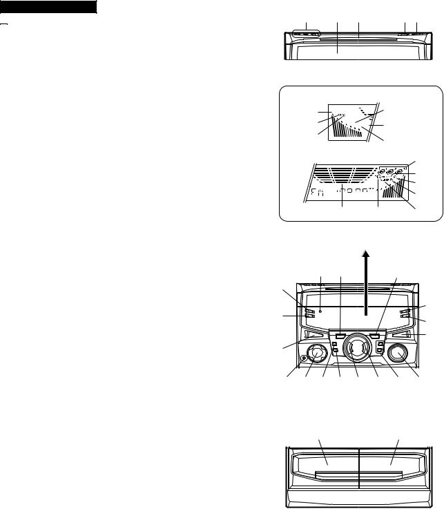
 Front Panel
1.Disc Number Selector Buttons
2.Disc Tray
3.Multi Indicator
4.Disc Skip Button
5.Open/Close Button
NAMES OF PARTS
1 |
2 |
3 |
4 5 |
6.Extra Bass Indicator
7.FM Stereo Mode Indicator
8.FM Stereo Indicator
9.(CD) Repeat Indicator
10.(CD) Play Indicator
11.(CD) Pause Indicator
12.(CD) Disc Number Indicators
13.(CD/TUNER) Memory Indicator
14.Timer Play Indicator
15.Timer Record Indicator
16.Sleep Indicator
16.Dynamic PTY Indicator
17.Spectrum Analyzer/ Volume Level Indicator
18.(TAPE 2) Racord Indicator
19.Timer Set Indicator
20.(CD) Track Down/Review Button (TUNER) Preset Down Button (TAPE 2) Rewind Button
21.(CD) Track Up/Cue Button (TUNER) Preset Up Button (TAPE 2) Fast Forward Button
22.Timer/Sleep Button
23.Clock Button
24.On/Stand-by Button
25.Equalizer Mode Selector Button
26.Dimmer Button
27.Extra Bass/Demo Mode Button
28.Headphone Socket
29.Function Selector Buttons
30.(TAPE 2) Record Pause Button
31.Memory/Set Button
32.(CD/TAPE) Stop Button
33.(TAPE) Play Button (CD) Play/Repeat Button
34.Tuning and Time Up/Down Buttons
35.Volume Up/Down Buttons
36.(TAPE 1) Cassette Compartment
37.(TAPE 2) Cassette Compartment
6
 9
9
7

 10
10
8 |
11 |
|
12
13
14


 15 17 18 16
19 20 |
21 |
|
22 |
|
|
23 |
25 |
|
26 |
||
|
||
24 |
27 |
|
|
28 29 30 31 32 33 34 35
36 37
– 4 –
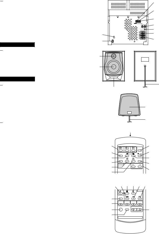

 Rear Panel
1.AC Voltage Selector
2.AC Power Input Socket
3.AM Aerial Terminal
4.Aerial Earth Terminal
5.FM 75 Ohms Aerial Socket
6.Video/Auxiliary (Audio Signal) Input Sockets
7.Span Selector Switch
8.Surround Speaker Terminals
9.Front Speaker Terminals
CP-C831

 Front Speaker
1.Tweeter
2.Woofer
3.Bass Reflex Ducts
4.Speaker Wire
GBOXS0025AWM1

 Surround Speaker
1.Full Range Speaker
2.Speaker Wire

 Remote Control
1. Remote Control Transmitter LED
 CD Control section
2.Disc Number Select Buttons
3.Memory Button
4.Pause Button
5.Clear Button
6.Track Down/Review Button
7.Track Up/Cue Button
8.Disc Skip Button
9.Play/Repeat Button
10.Stop Button
11.Random Button
 Tuner control section
12. Preset Up/Down Buttons
 Tape control section
13.(TAPE 1) Play Button
14.(TAPE 2) Record Pause Button
15.(TAPE 1/2) Stop Button
16.(TAPE 2) Play Button
17.(TAPE 2) Rewind Button
18.(TAPE 2) Fast Forward Button
 Common section
19.Equalizer Mode Selector Button
20.Function Selector Buttons
21.On/Stand-by Button
22.Extra Bass Button
23.Volume Up/Down Buttons
|
|
|
CD-C831W |
|
|
|
3 |
|
|
|
4 |
|
|
|
5 |
|
|
|
6 |
|
|
|
7 |
1 |
|
|
8 |
2 |
|
|
9 |
|
|
|
|
1 |
|
|
|
2 |
|
|
|
|
|
|
4 |
3 |
|
|
|
|
|
|
1 |
|
|
|
2 |
|
|
1 |
|
2 |
|
|
8 |
3 |
|
|
9 |
4 |
|
|
10 |
5 |
|
|
11 |
6 |
|
|
12 |
7 |
|
|
|
|
|
|
|
13 14 |
15 |
16 |
17 18 |
19 |
|
|
|
20 |
|
|
|
21 |
|
|
23 |
22 |
|
|
|
– 5 –

– 6 –
SETTING THE CLOCK
(Main unit operation)
In this example, the clock is set for the 24-hour (0:00) system.
CLOCK |
|
ON/ |
|
STAND-BY |
TUNING/ |
|
|
MEMORY/ |
TIME |
SET |
( ) |
|
2
3
4
0:00 AM 0:00 AM 12:00
5
6
7
8
9
1 |
Press the ON/STAND-BY button to enter the stand-by mode. |
||
2 |
Press the CLOCK button. |
|
|
3 |
Within 5 seconds, press the MEMORY/SET button. |
||
4 |
Press the TUNING/TIME ( |
or |
) button to select the time |
|
display mode. |
|
|
|
"0:00" → The 24-hour display will appear. |
||
|
(0:00 - 23:59) |
|
|
|
"AM 12:00" → The 12-hour display will appear. |
||
|
(AM or PM 12:00 - 11:59) |
||
|
"AM 0:00" → The 12-hour display will appear. |
||
|
(AM or PM 0:00 - 11:59) |
||
|
Note that this can only be set when the unit is first installed |
||
5 |
or it has been reset. |
|
|
Press the MEMORY/SET button. |
|
||
6 |
Press the TUNING/TIME ( |
or |
) button to adjust the hour. |
 Press the TUNING/TIME (
  or
or  ) button once to advance the time by 1 hour. Hold it down to advance continuously.
 When the 12-hour display is selected, "AM" will change automatically to "PM".
7 |
Press the MEMORY/SET button. |
8 |
Press the TUNING/TIME ( or ) button to adjust the |
|
minutes. |
 Press the TUNING/TIME (
  or
or  ) button once to advance the time by 1 minute. Hold it down to change the time in 5 minute intervals.
 The hour setting will not advance even if minutes advance from "59" to "00".
9 Press the MEMORY/SET button.
 The clock starts operating from "0" seconds. (Seconds are not displayed.)
To see the time display:
Press the CLOCK button.
 The time display will appear for about 5 seconds.
Note:
 The clock display will flash on and off at the push of the CLOCK button when the AC power supply is restored after a power failure occurs or after the AC power lead is disconnected.
If this happens, follow the procedure below to change the clock time.
To change the clock time:
1Press the CLOCK button.
2Within 5 seconds, press the MEMORY/SET button.
3Perform steps 6 - 9 above.
To change the time display mode:
1Perform steps 1 - 2 in the section "RESETTING THE MICROCOMPUTER".
2Perform steps 1 - 9 above.
PREPARATION FOR USE
0.2 m - 6 m (8" - 20')
15 |
15 |
 Remote control
Notes concerning use:
 Replace the batteries if the operating distance is reduced or if the operation becomes erratic.
 Periodically clean the transmitter LED on the remote control and the sensor on the main unit with a soft cloth.
 Exposing the sensor on the main unit to strong light may interfere with operation. Change the lighting or the direction of the unit.
 Keep the remote control away from moisture, excessive heat, shock, and vibrations.
C831W-CD
SPAN
RESETTING THE MICROCOMPUTER
2
1,2
 AM/FM interval (span)
The International Telecommunication Union (ITU) has established that member countries should maintain either a 10 kHz or a 9 kHz interval between broadcasting frequencies of any AM station. The illustration shows the 9 kHz interval zones (regions 1 and 3), and the 10 kHz interval zone (region 2).
Before using the unit, set the SPAN SELECTOR switch (on the rear panel) to AM tuning interval (span) of your area.
To change the tuning zone:
1 Press the ON/STAND-BY button to enter the stand-by mode.
2 Set the SPAN SELECTOR switch to "50/9" for 9 kHz AM interval (50 kHz FM interval), and "100/10" for 10 kHz AM interval (100 kHz FM interval).
3 Whilst pressing down the 

 button and the

 button, hold down the ON/STAND-BY button for at least 1 second.
Caution:
 The operation explained above will erase all data stored in memory including clock and timer settings, and tuner and CD presets.
Reset the microcomputer under the following conditions:
To erase all of the stored memory contents (clock and timer settings, and tuner and CD presets).
If the display is not correct.
If the operation is not correct.
1 Press the ON/STAND-BY button to enter the stand-by mode.
2 Whilst pressing down the 

 button and the

 button, hold down the ON/STAND-BY button for at least 1 second.
Caution:
The operation explained above will erase all data stored in memory including clock and timer settings, and tuner and CD presets.
MANUAL OPERATION

CD-C831W
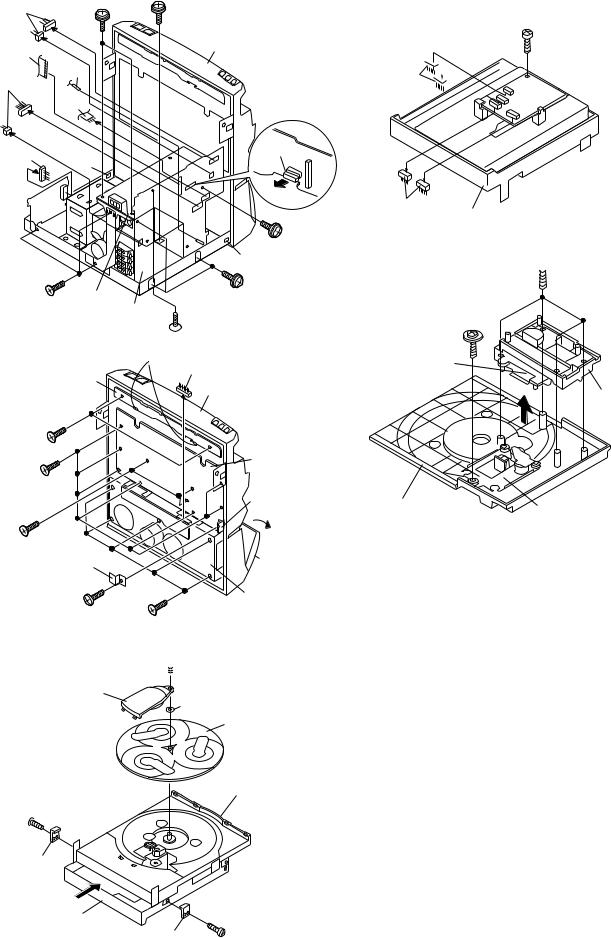
DISASSEMBLY
Caution on Disassembly
Follow the below-mentioned notes when disassembling the unit and reassembling it, to keep it safe and ensure excellent performance:
1.Take cassette tape and compact disc out of the unit.
2.Be sure to remove the power supply plug from the wall outlet before starting to disassemble the unit.
3.Take off nylon bands or wire holders where they need to be removed when disassembling the unit. After servicing the unit, be sure to rearrange the leads where they were before disassembling.
4.Take sufficient care on static electricity of integrated circuits and other circuits when servicing.
CD-C831W
STEP |
REMOVAL |
|
PROCEDURE |
|
FIGURE |
|
|
|
|
|
|
1 |
Top Cabinet |
1. |
Screw ..................... |
(A1) x4 |
7-1 |
|
|
|
|
|
|
2 |
Side Panel |
1. |
Screw ..................... |
(B1) x6 |
7-1 |
|
(Left/right) |
2. Hook ....................... |
(B2) x2 |
|
|
|
|
|
|
|
|
3 |
CD Player Unit/ |
1. |
Turn on the power supply, |
7-2 |
|
|
CD Tray Cover |
|
open the disc tray, take out |
|
|
|
|
|
the CD cover, and close. |
|
|
|
|
|
(Note 1) |
|
|
|
|
2. |
Hook ....................... |
(C1) x3 |
|
|
|
3. |
Hook ....................... |
(C2) x2 |
|
|
|
4. |
Socket .................... |
(C3) x2 |
|
|
|
|
|
|
|
4 |
Back Board |
1. |
Screw ..................... |
(D1) x6 |
7-2 |
|
|
|
|
|
|
5 |
Tuner PWB |
1. |
Screw ..................... |
(E1) x3 |
8-1 |
|
|
2. |
Socket .................... |
(E2) x1 |
|
|
|
|
|
|
|
6 |
Main PWB |
1. |
Screw ..................... |
(F1) x4 |
8-1 |
|
|
2. |
Socket .................... |
(F2) x4 |
|
|
|
3. |
Flat Wire ................. |
(F3) x1 |
|
|
|
4. |
Tip Wire .................. |
(F4) x1 |
|
|
|
5. |
Flat Cable ............... |
(F5) x1 |
|
|
|
|
|
|
|
7 |
Front Panel |
1. |
Screw ..................... |
(G1) x1 |
8-1 |
|
|
2. |
Socket .................... |
(G2) x1 |
|
|
|
3. |
Hook ....................... |
(G3) x2 |
|
|
|
|
|
|
|
8 |
Headphones PWB |
1. |
Screw ..................... |
(H1) x1 |
8-2 |
|
|
2. |
Support Bracket ..... |
(H2) x1 |
|
|
|
|
|
|
|
9 |
Display PWB/ |
1. Screw ..................... |
(J1) x12 |
8-2 |
|
|
Switch PWB |
2. |
Hook ....................... |
(J2) x2 |
|
|
|
3.Socket ..................... |
(J3) x1 |
|
|
|
|
|
|
|
|
10 |
Tape Mechanism |
1. |
Open the cassette holder. |
8-2 |
|
|
|
2. |
Screw...................... |
(K1) x5 |
|
|
|
|
|
|
|
11 |
Turntable |
1. |
Screw ..................... |
(L1) x1 |
8-3 |
|
|
2. |
Cover ..................... |
(L2) x1 |
|
|
|
|
|
|
|
12 |
Disc Tray |
1. Screw ..................... |
(M1) x2 |
8-3 |
|
|
|
2. |
Guide ..................... |
(M2) x2 |
|
|
|
|
|
|
|
13 |
CD Servo PWB |
1. |
Screw ..................... |
(N1) x1 |
8-4 |
|
(Note 2) |
2. |
Socket .................... |
(N2) x4 |
|
|
|
|
|
|
|
14 |
CD Changer |
1. |
Screw ..................... |
(P1) x4 |
8-5 |
|
Mechanism |
|
|
|
|
|
|
|
|
|
|
15 |
CD Mechanism |
1. |
Screw ..................... |
(Q1) x1 |
8-5 |
|
|
|
|
|
|
Note 1:
How to open the changer manually. (Fig. 7-3)
1.Turn fully the lock lever in the arrow direction through the hole on the loading chassis bottom in this state.
After that, push forward the CD player base.
Note 2:
1.After removing the connector for the optical pickup from the connector, wrap the conductive aluminium foil around the front end of connector to protect the optical pickup from electrostatic damage.
CD-C831W
Top Cabinet
(A1) x2 ø3x12mm
(B2) x1
(B1) x1 ø3x10mm
Side Panel (Right)
|
(A1) x2 |
|
|
ø3x12mm |
|
Back Board |
Side Panel |
|
|
(Left) |
|
(B1) x4 |
(B2) x1 |
|
|
||
ø3x8mm |
(B1) x1 |
|
|
ø3x10mm |
|
|
Figure 7-1 |
|
(C2) x1 |
CD Tray Cover |
|
(C1) x3 |
||
Pull |
||
1 |
||
(C3) x2 |
1
CD Player 
 2 Unit
(C2) x1
Back Board
Main PWB

 (D1) x6 ø3x10mm
Figure 7-2
LOCK
LEVER
Figure 7-3
– 7 –
CD-C831W
|
(E1) x2 |
|
(F2) x2 |
ø3x10mm |
(F1) x1 |
|
ø3x10mm
Front Panel
(F5) x1
 (F4) x1
(F2) x2
(F3)x1
(E2) x1
(G2) x1 |
(G3) x1 |
|
|
(E1) x1 |
|
|
|
ø3x10mm |
|
|
|
(G3) x1 |
|
|
|
(F1) x3 |
|
Tuner PWB |
ø3x10mm |
||
|
|||
|
Main PWB |
(G1) x1 |
|
|
|
ø3x10mm |
|
|
Figure 8-1 |
||
|
(J2)x2 |
|
|
Switch PWB |
|
(J3)x1 |
|
|
|
||
|
|
Front Panel |
|
(J1)x2 |
|
|
|
ø3x10mm |
|
|
|
|
|
Display PWB |
|
(J1)x7 |
|
|
|
ø3x10mm |
|
Headphones |
|
|
|
||
|
|
PWB |
|
|
|
Open |
|
(J1)x3 |
|
|
|
ø3x10mm |
|
Cassette |
|
(H2)x1 |
|
Holder |
|
|
|
||
(H1)x1 |
|
Tape Mechanism |
|
ø3x10mm |
|
||
(K1)x5 |
|||
|
|||
|
ø3x10mm |
||
Figure 8-2
 (L1) x1
  ø3 x10mm
(L2) x1
Washer
Turntable
Disc Tray
(M1) x1  ø3 x10mm
(M2) x1
|
(M1) x1 |
CD Player Unit |
ø3 x10mm |
(M2) x1
Figure 8-3
(N1) x1 ø3 x10mm
 CD Servo PWB (N2) x2

(N2) x2
CD Player Unit
Figure 8-4
 (P1) x4
ø3 x12mm
(Q1) x1 ø2.6 x10mm
Shift Lever
CD Changer
Mechanism
CD Player Base |
CD Mechanism |
Be Careful when installing the CD changer mechanism. Install the CD changer mechanism on the CD player base after the shift lever has been set in the highest position.
Figure 8-5
– 8 –
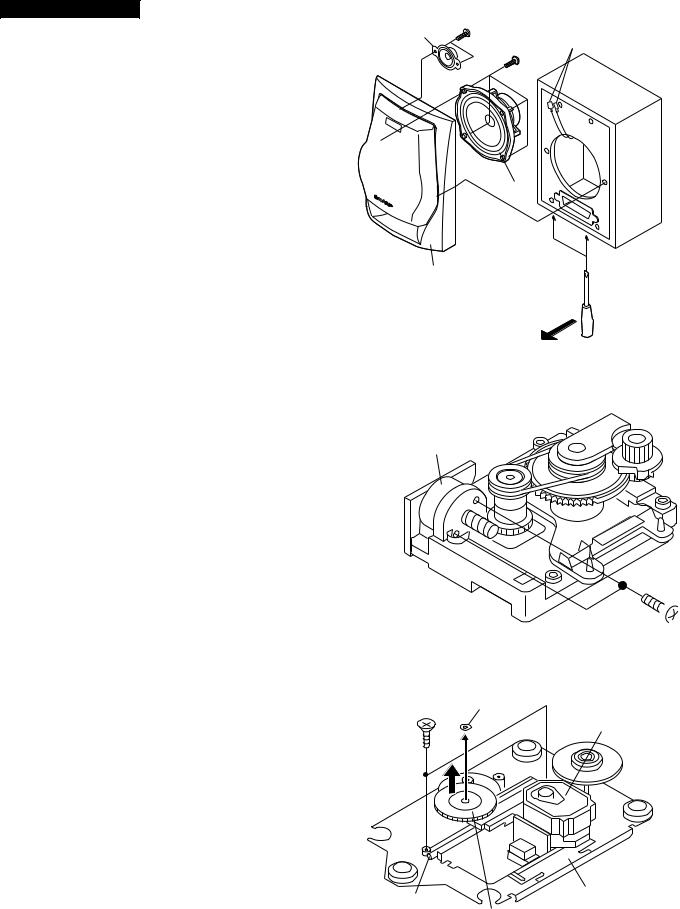
CD-C831W
CP-C831
STEP |
REMOVAL |
|
PROCEDURE |
|
FIGURE |
|
|
|
|
|
|
1 |
Front Speaker |
1. Front Panel ............ |
(A1) x1 |
9-1 |
|
|
|
2. |
Tip .......................... |
(A2) x2 |
|
|
|
3. |
Screw ..................... |
(A3) x6 |
|
|
|
|
|
|
|
Note:
The Surround speakers can be easily disassembled. Therefore the disassembling method is not described.
For details refer to the disassembling drawing in the Parts Guide.
(A3)x2
ø3x10mm
Tweeter |
(A3)x4 |
(A2)x2 |
|
ø4x12mm |
|
Woofer
Front Panel
(A1)x1
Screw Driver
Figure 9-1
REMOVING AND REINSTALLING THE MAIN PARTS
CD MECHANISM SECTION
Perform steps 1, 2, 3, 11, 12, 13, 14 and 15 of the disassembly method to remove the CD mechanism.
How to remove the loading motor (See Fig. 9-2)
1.Remove the screws (A1) x 2 pcs., to remove the loading motor.
How to remove the pickup (See Fig. 9-3)
1.Remove the screws (B1) x 2 pcs., to remove the shaft (B2).
2.Remove the stop washer (B3) x 1 pc., to remove the gear (B4).
3.Remove the pickup.
Note
After removing the connector for the optical pickup from the connector, wrap the conductive aluminium foil around the front end of connector to protect the optical pickup from electrostatic damage.
Loading Motor
Motor
PWB 
(A1) x2  ø2.6 x5mm
Figure 9-2
(B1) x2
Stop Washer
ø2.6 x6mm
(B3) x1
Pickup
Shaft |
CD Mechanism |
|
Gear |
||
(B2) x1 |
||
(B4) x1 |
||
|
||
|
Figure 9-3 |
– 9 –
CD-C831W
ADJUSTMENT
MECHANISM SECTION
∙ Driving Force Check
|
Torque Meter |
|
|
Specified Value |
|||||
|
|
|
|
|
|||||
Play: TW-2412 |
|
Tape 1: Over 80 g |
|
|
|||||
|
|
|
|
Tape 2: Over 80 g |
|
|
|||
|
|
|
|
|
|
|
|
|
|
∙ Torque Check |
|
|
|
|
|
|
|
||
|
|
|
|
|
|
|
|||
Torque Meter |
|
Specified Value |
|||||||
|
|
|
|
|
|
|
|
|
|
|
|
|
Tape 1 |
|
|
|
Tape 2 |
||
|
|
|
|
||||||
Play: TW-2111 |
30 to 60 g. cm |
|
30 to 100 g.cm |
||||||
|
|
|
|
|
|||||
Fast forward: TW-2231 |
— |
|
|
50 to 100 g.cm |
|||||
|
|
|
|
|
|||||
Rewind: TW-2231 |
— |
|
|
50 to 100 g.cm |
|||||
|
|
|
|
|
|
|
|
|
|
∙ Tape Speed |
|
|
|
|
|
|
|
||
|
|
|
|
|
|
|
|
|
|
|
|
Test Tape |
Adjusting |
Specified |
|
Instrument |
|||
|
|
|
Point |
|
Value |
|
Connection |
||
|
|
|
|
|
|
|
|||
Normal |
|
MTT-111 |
VRM1 |
3,000 ± |
|
Speaker |
|||
speed |
|
|
|
|
30 Hz |
|
terminal |
||
|
|
|
|
|
|
|
|
|
|
TUNER SECTION
fL: Low-range frequency fH: High-renge frequency
∙ AM IF/RF
Signal generator: 400 Hz, 30%, AM modulated
Test Stage |
Frequency |
Frequency |
Setting/ |
Instrument |
|
|
|
|
Display |
Adjusting |
Connection |
|
|
|
|
Parts |
|
|
|
|
|
|
|
IF |
450 kHz |
|
1,602 kHz |
T351 |
*1 |
|
|
|
|
|
|
AM Band |
— |
|
531 kHz |
(fL): T306 |
*2 |
Coverage |
|
|
|
1.1 ± 0.1 V |
|
|
|
|
|
|
|
AM |
990 kHz |
|
990 kHz |
(fH): T302 |
*1 |
Tracking |
|
|
|
|
|
|
|
|
|
|
|
*1. Input: Antenna, |
Output: TP302 |
|
|
||
*2. Input: Antenna, |
Output: TP301 |
|
|
||
•FM Notes:
1: Description of the "FM IF Adjustment" is not carried on this Manual. It is because the IF coil in the FM front end section has been best adjusted in the factory so that its further adjustment is not needed at the field. When replacing the FM front end assembly, no adjustment is needed either.
2: The parts in the FM front end section are prepared in a complete unit, so you can't obtain each part individually
•FM Mute Level
Signal generator: 1 kHz, 40 kHz dev., FM modulated
Frequency |
Frequency |
Adjusting |
Instrument |
|
Display |
Parts |
Connection |
98.00 MHz |
98.00 MHz |
VR351 |
Input: Antenna |
(25 dBμV) |
|
|
Output: Speaker |
|
|
|
Terminal |
CD ERROR CODE DESCRIPTION
When a malfunction occurs during CD operation, an error code will be displayed to identify the function in CD operation which failed.
Error |
State Code |
|
|
0001 |
Cannot detect pickup-in SW |
|
|
0101 |
Tray close operation error |
|
|
0105 |
Tray close operation error |
|
|
0201 |
Tray open operation error |
|
|
0203 |
Tray open operation error |
|
|
0304 |
Disc skip operation error |
|
|
0305 |
Disc skip operation error |
|
|
0307 |
Disc skip operation error |
|
|
TAPE MECHANISM PWB
VRM1
SWM1
TAPE
FAS SPEED
SW
|
|
|
|
TUNER PWB |
|
||
|
|
|
|
|
TP301 |
SO301 |
|
|
|
|
|
|
R336 |
|
|
|
|
|
VR351 |
|
|
ANTENNA |
|
|
|
T351 |
|
|
|
||
|
|
|
|
|
|
TERMINAL |
|
|
|
AM IF |
|
|
|
|
|
|
|
FM MUTE |
|
FE301 |
|
|
|
|
IC303 |
|
|
|
|
||
TP302 |
|
|
|
|
|
||
|
LEVEL |
|
|
|
|
||
R357 |
|
|
T306 |
T302 |
AM |
|
|
|
|
|
|
|
|||
|
|
|
AM BAND |
|
|||
|
|
|
TRACKING |
|
|||
|
|
|
COVERAGE |
|
|||
|
|
|
|
|
|||
|
Figure 10 ADJUSTMENT POINTS |
|
|
||||
|
|
|
– 10 – |
|
|
|
|
CD-C831W
TEST MODE
• Setting the test mode
Any one of test mode can be set by pressing several keys as follows. <REC. PAUSE> + <DISC. SKIP> + <POWER> TEST: CD operation test
• TEST mode
Function — CD test mode
Setting of TEST mode
Indication of CD TST mode (Fig. 11-1)
|
OPEN/CLOSE operation is manual operation. |
) or ( |
) key. |
|
IL is not performed. |
||||||
|
|||||||||||
|
|
|
|
|
|||||||
|
|
|
|
|
|
|
|||||
The pickup can be moved by using the ( |
|
|
|||||||||
|
|
|
|||||||||
|
|
<MEMORY> |
|
<MEMORY> |
|
<MEMORY> |
<STOP> |
||||
|
|
LASER ON |
|
Tracking on the spot. |
|
|
Tracking on the spot. |
|
STOP |
||
|
|
|
|
SERVO OFF PLAY |
|
|
SERVO ON PLAY |
|
|
||
|
|
<PLAY> key input |
|
TOC. IL is performed, and the ordinary PLAY is performed. |
|
Press <STOP> key. |
|
Stop |
||||
|
|
|
|
|
||||||||
|
|
|
|
If the following key is pressed during PLAY, it is possible |
|
|
|
|
||||
|
|
|
|
to specify directly any Track No. |
|
|
|
|
|
|
|
|
|
|
|
|
<Disc Number 1> key: Track 4 |
|
|
|
|
|
|
|
|
|
|
|
|
<Disc Number 2> key: Track 9 |
|
|
|
|
|
|
|
|
|
|
|
|
<Disc Number 3> key: Track 15 |
|
|
|
|
|
|
|
|
Note: |
|
|
|
|
|
|
|
|
|
|
||
Only in STOP state it is possible to slide the pickup with the ( |
) or ( |
) key. |
|
|
|
|
||||||
VOL. --- Last memory |
|
|
|
|
|
|
|
|
|
|
||
BAL. --- CENTER |
|
|
1 |
2 |
3 |
|
|
|
|
|
||
R.GEQ. --- FLAT |
|
|
|
|
|
|
||||||
X-BAS --- OFF |
|
|
|
|
|
|
|
|
|
|
||
Canceling method - POWER OFF |
|
|
|
|
|
|
|
|
||||
|
|
|
|
|
|
|
|
|
|
|
|
|
Figure 11-1
CD SECTION
Since this CD system incorporates the following automatic adjustment function, when the pickup is replaced, it is not necessary to readjust it.
Since this CD unit does not need adjustment, the combination of PWB and laser pickup unit is not restricted.
• Automatic adjustment item
1.Focus offset (Fig. 11-2)
2.Tracking offset (Fig. 11-3)
3.E/F balance (tracking error balance) (Fig. 11-4)
4.RF level AGC function (HF level: constant)
5.RF level automatic follow-up of the tracking gain
This automatic adjustment is performed each time a disc is changed. Therefore, each disc is played back using the optimal settings.
0.1s |
|
|
0.50 V |
|
|
IC1 20 |
FE |
|
|
|
FOCUS |
|
|
OFF-SET |
|
|
ADJUST |
0.1s |
|
|
0.50 V |
|
|
IC1 7 |
TE |
TRACKING |
|
|
|
|
|
OFF-SET |
|
|
1 ADJUST |
|
2 |
|
|
Figure 11-2 |
|
200 ms |
TRACKING/ |
|
1V/diV |
ERROR |
|
IC 1 15 |
BARANCE |
|
TO |
1 ADJUST |
|
|
||
200 ms |
|
|
1V/diV |
|
|
IC 1 7 |
2 |
|
TE |
||
|
||
|
Figure 11-4 |
10ms 0.50 V
IC1 20 FE
10ms 0.50 V IC1 7 TE
Figure 11-3
Enlarged
View
TRACKING
OFF-SET 1 ADJUST
2
– 11 –
CD-C831W
NOTES ON SCHEMATIC DIAGRAM
∙Resistor:
To differentiate the units of resistors, such symbol as K and M are used: the symbol K means 1000 ohm and the symbol M means 1000 kohm and the resistor without any symbol is ohm-type resistor. Besides, the one with “Fusible” is a fuse type.
∙Capacitor:
To indicate the unit of capacitor, a symbol P is used: this symbol P means micro-micro-farad and the unit of the capacitor without such a symbol is microfarad. As to electrolytic capacitor, the expression “capacitance/withstand voltage” is used.
(CH), (TH), (RH), (UJ): Temperature compensation (ML): Mylar type
(P.P.): Polypropylene type
∙Schematic diagram and Wiring Side of P.W.Board for this model are subject to change for improvement without prior notice.
∙The indicated voltage in each section is the one measured by Digital Multimeter between such a section and the chassis with no signal given.
1.In the tuner section, ( ) indicates AM
< > indicates FM stereo
2.In the main section, a tape is being played back.
3.In the deck section, a tape is being played back. ( ) indicates the record state.
4.In the power section, a tape is being played back.
5.In the CD section, the CD is stopped.
∙Parts marked with “ ” (
” ( 


 ) are important for maintaining the safety of the set. Be sure to replace these parts with specified ones for maintaining the safety and performance of the set.
REF. NO |
|
|
|
|
|
|
|
|
DESCRIPTION |
POSITION |
||||||
|
|
|
|
|
|
|
|
|
|
|
|
|
|
|
||
SW1 |
OPEN/CLOSE |
ON—OFF |
||||||||||||||
|
|
|
|
|
|
|
|
|
|
|
|
|
|
|
||
SW2 |
MECHA UP |
ON—OFF |
||||||||||||||
|
|
|
|
|
|
|
|
|
|
|
|
|
|
|
||
SW3 |
DISC NUMBER |
ON—OFF |
||||||||||||||
|
|
|
|
|
|
|
|
|
|
|
|
|
|
|
||
SW4 |
PICKUP IN |
ON—OFF |
||||||||||||||
|
|
|
|
|
|
|
|
|
|
|
|
|
|
|
||
SW601 |
SPAN SELECTOR |
100/10 –50/9 |
||||||||||||||
|
|
|
|
|
|
|
|
|
|
|
|
|
|
|
||
SW701 |
ON/STAND-BY |
ON—OFF |
||||||||||||||
|
|
|
|
|
|
|
|
|
|
|
|
|
|
|
|
|
SW703 |
CLOCK |
|
|
|
|
ON—OFF |
||||||||||
|
|
|
|
|
|
|
|
|
|
|
|
|
|
|
||
SW704 |
TIMER/SLEEP |
ON—OFF |
||||||||||||||
|
|
|
|
|
|
|
|
|
|
|
|
|
|
|
|
|
SW705 |
DISC 1 |
|
|
|
|
ON—OFF |
||||||||||
|
|
|
|
|
|
|
|
|
|
|
|
|
|
|
|
|
SW706 |
DISC 2 |
|
|
|
|
ON—OFF |
||||||||||
|
|
|
|
|
|
|
|
|
|
|
|
|
|
|
|
|
SW707 |
DISC 3 |
|
|
|
|
ON—OFF |
||||||||||
|
|
|
|
|
|
|
|
|
|
|
|
|
|
|
||
SW708 |
DISC SKIP |
ON—OFF |
||||||||||||||
|
|
|
|
|
|
|
|
|
|
|
|
|
|
|
||
SW709 |
OPEN/CLOSE |
ON—OFF |
||||||||||||||
|
|
|
|
|
|
|
|
|
|
|
|
|
|
|
|
|
SW710 |
REV |
|
|
|
|
|
|
|
ON—OFF |
|||||||
|
|
|
|
|
|
|
|
|
|
|
|
|
|
|
||
SW711 |
REC PAUSE |
ON—OFF |
||||||||||||||
|
|
|
|
|
|
|
|
|
|
|
|
|
|
|
||
SW712 |
MEMORY/SET |
ON—OFF |
||||||||||||||
|
|
|
|
|
|
|
|
|
|
|
|
|
|
|
|
|
SW713 |
STOP |
|
|
|
|
ON—OFF |
||||||||||
|
|
|
|
|
|
|
|
|
|
|
|
|
|
|
||
SW714 |
TUNER/BAND |
ON—OFF |
||||||||||||||
|
|
|
|
|
|
|
|
|
|
|
|
|
|
|
|
|
|
|
|
|
|
|
|
|
|
|
|
|
|
|
|
|
|
|
|
|
FRONT |
|
|
FRONT |
|
|||||||||
|
|
|
|
|
VIEW |
|
||||||||||
|
|
|
|
VIEW |
|
|
|
|
|
|
||||||
|
|
|
|
|
|
|
|
|
|
|
|
|
||||
|
|
|
|
|
|
|
|
|
|
|
|
|
|
|
|
|
|
|
|
|
|
|
|
|
|
|
|
|
|
|
|
|
|
|
|
|
|
|
|
|
|
|
|
|
|
|
|
|
|
|
|
|
|
|
|
|
|
|
|
|
|
|
|
B C E |
|||
|
|
|
|
|
|
|
|
|
|
|
|
|
(D)(G)(S) |
|||
|
|
E |
|
C |
|
B |
(3) (2) (1) |
|
||||||||
|
|
(S) |
(G) |
(D) |
|
|
|
|
|
|||||||
|
(1) |
(2) |
(3) |
|
|
|
|
|
|
|||||||
REF. NO |
DESCRIPTION |
POSITION |
|
|
|
SW715 |
VIDEO |
ON—OFF |
|
|
|
SW716 |
TAPE |
ON—OFF |
|
|
|
SW717 |
CD |
ON—OFF |
|
|
|
SW721 |
DISPLAY MODE |
ON—OFF |
SW722 |
FF |
ON—OFF |
|
|
|
SW723 |
TUNING UP |
ON—OFF |
|
|
|
SW724 |
TUNING DOWN |
ON—OFF |
|
|
|
SW725 |
PLAY |
ON—OFF |
|
|
|
SW726 |
VOLUME DOWN |
ON—OFF |
|
|
|
SW727 |
VOLUME UP |
ON—OFF |
|
|
|
SW728 |
X-BASS/DEMO |
ON—OFF |
|
|
|
SW729 |
EQUALIZER |
ON—OFF |
|
|
|
SW730 |
DIMMER |
ON—OFF |
|
|
|
SW801 |
VOLTAGE SELECTOR |
110/127/220/ |
|
|
230–240V |
|
|
|
SWM 3 |
FOOL PROOF |
ON—OFF |
|
|
|
SWM 4 |
F.A.S. |
ON—OFF |
|
|
|
SWM 5 |
CAM |
ON—OFF |
|
|
|
FRONT VIEW
1 2 3
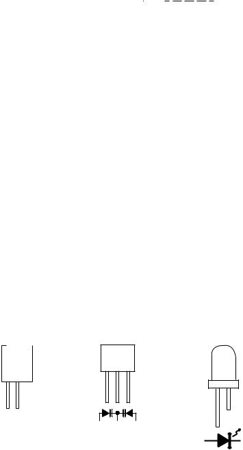
2SA1015 GR |
KTA1266 GR |
2SA1318 |
SVC348S |
L1154GT4 |
2SA1318 |
KTA1271 Y |
|
|
SLI342YCB |
2SC2389 SE |
KTA1273 Y |
|
|
SLI342DCB |
2SC3331 |
KTA1274 Y |
|
|
SLI342UCB |
KRC102 M |
KTD2058 Y |
|
|
SLI342UCB |
KRC104 M |
KTC3199 GR |
|
|
SLI342YCJ |
KRC107 M |
KTC3203 Y |
|
|
|
Figure 12 TYPES OF TRANSISTOR AND LED
– 12 –
|
|
|
|
|
|
|
|
|
|
|
|
|
|
|
|
CD-C831W |
|
|
|
|
|
|
|
|
|
SW2 |
MECHA UP SW3 |
DISC No. |
SW1 OPEN/CLOSE M3 |
LOADING |
SOLM1 |
|
|
|
|
|
|
|
|
|
|
|
|
|
|
M |
|
|
|
|
|
|
|
|
|
|
|
|
|
|
|
|
|
|
|
|
TO MAIN |
|
|
|
|
|
|
|
|
|
|
|
|
|
|
|
CNS10 |
SECTION |
|
|
|
|
|
|
|
|
|
10 9 8 |
7 6 5 4 3 |
2 1 |
|
||||
|
|
TO MAIN SECTION |
|
|
|
|
|
OPEN/CLOSE GND (D) M– |
|
|
|
|||||
|
|
|
|
|
|
|
|
|
|
|
||||||
|
|
(TO IC601) |
|
|
|
GND (D) |
MECHA UP GND (D) |
DISK NO. |
|
GND (M) |
|
+7.3V (B1) |
||||
|
|
|
|
CNP11 |
|
|
|
M+ |
CNP10 |
|
||||||
|
|
1 2 3 4 5 6 |
|
|
|
|
10 9 8 |
7 6 5 4 3 |
2 1 |
|
||||||
|
|
|
|
|
|
|
|
|
|
|
|
|
|
|
REGULATOR |
|
|
|
|
|
|
|
|
|
|
|
|
|
|
|
|
|
|
|
|
|
|
|
|
|
|
|
|
|
|
|
|
|
|
Q81 |
|
|
|
|
|
|
|
|
|
|
|
|
|
|
|
|
+4.3V |
|
|
|
|
|
Q51 |
|
|
|
|
|
|
|
|
|
|
|
|
|
33 38 39 46 |
37 38 39 40 |
27 |
24 |
25 |
|
|
|
|
|
|
|
|
|
|
|
43 XVDD |
LCHO LVSS RVSS |
RCHO |
|
CONT1 |
CONT2 |
|
|
|
|
|
|
|
|
|
|
|
41 RVDD |
|
|
|
|
|
|
|
|
|
|
|||||
+5V |
36 LVDD |
|
|
|
|
|
|
|
|
|
|
|
|
|
|
|
|
23 VDD |
IC2 |
|
|
RES. CQCK. COIN SQOUT. RWC. WRQ |
26 |
|
|
|
|
|
|
|
|
||
|
6 VVDD |
|
|
|
|
|
|
|
|
|
|
|
||||
|
LC78622NE |
|
|
|
|
|
|
|
|
|
|
|||||
|
|
|
|
58 |
|
|
|
|
|
|
|
|
||||
|
|
SERVO/SIGNAL |
|
|
|
|
|
|
|
|
||||||
|
|
~ |
|
|
|
|
|
|
|
|
||||||
|
44 |
|
CONTROL |
|
53 |
|
|
|
|
|
|
|
|
|||
|
|
|
|
|
|
|
|
|
|
|
|
|||||
XL1 |
|
|
|
|
|
|
64 |
|
|
|
|
|
|
|
|
|
|
45 |
|
|
EFMO EFMIN |
CLV+ |
|
~ |
CONTROL/CE |
|
|
|
|
|
|
|
|
|
|
|
JP– |
62 |
|
|
|
|
|
|
|
|||||
|
|
|
|
|
|
|
|
|
|
|
||||||
|
|
|
|
51 |
|
|
|
|
|
|
|
|||||
|
|
2 |
4 8 11 |
9 10 12 ~ |
20 |
|
|
|
|
|
|
|
|
|||
|
|
XOUTXIN |
|
|
|
|
|
|
|
|
|
|
|
|
||
+B1 |
|
|
|
|
|
|
|
|
CL, DAT, SELIAL |
|
|
|
|
|
|
PU-IN SW |
|
|
22 |
32 ~ |
40 43 44 |
|
|
|
|
+B1 |
|
|
|
||||
|
|
|
|
JP– |
CV+ SLC |
SL1 |
CE 53 |
|
|
+B5 |
|
|||||
Q52 |
|
|
|
|
|
|
|
|||||||||
|
|
|
DAT 52 |
|
|
|
|
|
|
|||||||
|
|
|
|
|
|
|
|
|
|
|
|
|
|
|
||
|
|
|
|
|
|
|
CL 51 |
|
|
|
|
|
|
|
|
|
|
|
|
|
IC1 |
|
|
DRF 54 |
SL+. SL–. DRF |
42 41 |
20 40 24 18 |
28 39 38 37 36 |
|
||||
|
|
VCC1 |
|
|
|
|
|
|
|
|
|
|
||||
+5V |
64 |
|
|
|
SL+ 31 |
|
|
|
|
|
|
|
|
|||
LA9241M |
|
SL– 30 |
|
|
|
IC3 |
|
|
35 |
|||||||
|
|
|
|
|
|
|
|
|||||||||
|
|
SERVO AMP. |
|
|
|
|
|
M63001FP |
|
~ |
||||||
|
|
|
SLD 29 |
|
|
|
|
29 |
||||||||
|
|
|
|
|
|
|
25 |
|
|
FOCUS/ |
|
22 |
||||
|
|
|
|
|
|
|
NC 23 |
20 |
|
|
TRACKING/ |
|
||||
|
|
LD0 |
|
|
|
|
|
|
|
|
||||||
|
|
|
|
|
|
7 |
|
|
|
21 |
||||||
Q1 |
62 |
|
|
|
|
SPO 27 |
|
|
SPIN/SLED |
|
||||||
|
|
|
|
|
|
|
14 |
|||||||||
|
|
|
|
FIN2 |
FIN1 E |
|
FD 16 |
2 |
|
|
DRIVER |
|
||||
|
|
|
|
F |
|
15 |
1 |
|
|
|
~ |
|||||
|
|
|
|
1 2 3 4 |
|
|
|
|
|
|
|
|
|
8 |
||
|
|
|
|
|
|
|
23 |
|
6 7 4 5 |
15 16 26 27 |
|
|||||
M1
SPINDLE
MOTOR
UNIT |
|
|
M |
COILFOCUS |
COILTRACKING |
|
|
PICKUP |
M2 |
||
|
|
|
SLED |
|
|
|
MOTOR |
|
|
|
M |
PICKUP IN
SW4
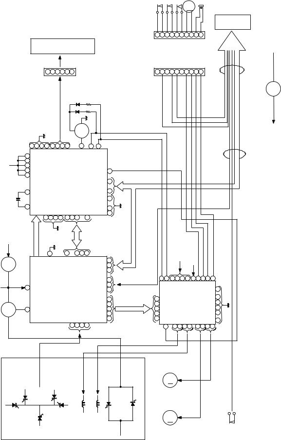
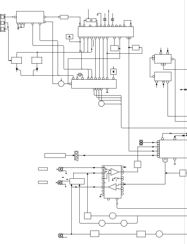
Figure 13 BLOCK DIAGRAM (1/3)
– 13 –
CD-C831W
SO301 |
|
|
|
|
|
|
|
|
|
|
|
+B4 |
|
|
|
|
|
DETFM |
CF351 |
+B4 |
X351 456kHz |
|
|
|
|
||
|
|
|
|
|
|
|
|
|
|
|
|
|
|
|
|
|
|
|
|
|
|
|
|
|
|
|
|
ANTENNA |
|
|
|
|
|
|
|
|
|
|
|
|
|
|
|
|
|
|
|
|
|
|
|
|
|
|
|
TERMINAL |
|
|
|
|
|
|
FM IF |
|
|
|
|
|
|
|
|
|
|
|
|
|
|
|
|
|
|
|
|
FM |
|
|
|
FE301 |
|
|
|
|
|
|
|
|
|
|
|
|
|
|
|
|
|
|
|
|
|
|
|
8 |
|
|
|
1 |
CF302 |
|
|
|
AM IF |
|
|
|
|
|
|
|
|
|
|
|
|
|
|
|
|||
75 ohms |
FM FRONT END |
|
|
|
|
|
|
|
|
|
|
|
|
|
|
|
|
|
|
||||||||
|
|
|
|
|
|
|
|
T351 |
CF352 |
|
|
|
|
|
|
|
|
|
|
|
|||||||
|
|
|
|
|
|
5 |
|
FM IF IN |
|
|
|
|
|
|
|
|
|
|
|
|
|||||||
GND |
2 |
6 |
7 |
3 |
4 |
|
|
|
|
|
|
|
|
|
|
|
|
|
|
|
|
|
|
||||
|
|
|
|
|
|
|
|
|
|
|
|
|
|
|
|
|
|
|
|
|
|
||||||
|
|
|
|
|
|
|
|
|
|
|
|
|
|
|
|
|
|
|
|
|
|
|
|||||
|
|
|
|
OUT OSC |
VT |
|
|
|
|
1 |
2 |
|
3 |
|
|
4 |
|
5 |
8 |
|
9 |
17 |
19 |
20 |
18 |
16 |
|
AM |
|
|
|
|
|
|
|
|
OUT |
|
REG |
|
IN GND |
|
|
VCC |
|
|
|
FM/AM |
MPX |
||||||
|
|
|
|
F |
|
|
|
|
|
|
|
|
|
IC303 |
|
|
|
|
|
|
|
OUT |
IN |
||||
|
|
|
|
|
|
|
VR351 |
|
|
|
|
|
|
|
|
|
|
|
|
||||||||
|
|
|
|
|
|
|
|
|
|
|
|
LA1832 |
|
|
|
|
|
|
|
|
|
||||||
|
|
|
|
|
|
|
FM MUTE LEVEL |
|
|
|
|
|
|
|
|
|
|
|
|
|
|
||||||
|
|
|
|
|
|
|
|
|
|
AM OSC FM/AM IF MPX. OUTIF |
|
|
|
|
|
||||||||||||
|
|
|
|
|
|
|
|
|
|
24 |
23 |
22 |
|
21 |
|
7 |
13 |
6 |
|
|
10 |
11 |
|
12 |
MPX |
14 15 |
|
|
|
|
|
|
|
|
|
|
|
OUT |
IN |
AFC |
RFAMIN |
STEREO |
MONO/ST |
|
SD |
|
|
|
Q361 |
|
Q353 |
||||
|
|
|
|
|
|
|
|
|
|
|
|
|
|
|
|
|
|
|
|
|
|
|
|
|
|
|
L R |
|
|
|
|
|
|
|
FMOSC |
|
|
|
|
|
|
|
|
|
|
|
|
|
|
|
|
|
|
|
MUTING |
|
|
|
|
|
|
|
|
|
|
|
|
|
|
|
|
|
|
|
|
|
|
|
MPX |
|
VCO |
Q354 |
|
|
AM RF |
|
|
|
|
|
|
|
|
|
|
|
|
|
|
|
|
|
|
|
|
PHASE |
|
CUT |
TUNER MUTE |
||
|
|
|
|
|
|
|
|
|
|
|
|
|
|
|
|
|
|
|
|
|
|
|
|
||||
|
|
|
|
|
|
|
|
|
|
|
|
|
|
|
|
|
|
|
|
|
|
|
|
|
|
|
|
|
AM ANT |
|
AM OSC |
|
|
|
|
|
|
|
|
|
|
|
|
|
|
|
|
|
|
|
|
|
|||
|
T302 |
|
|
|
T306 |
|
|
|
|
|
|
|
|
|
|
|
|
|
|
|
|
VOLTAGE |
|
|
|
||
|
|
|
|
|
|
|
|
|
|
|
|
|
|
|
|
|
|
|
|
|
|
REGURATER |
|
|
|
||
|
|
|
|
|
|
|
|
|
|
|
|
|
|
|
|
|
MONO/STFM |
|
|
|
|
|
+B4 |
|
|
|
|
|
|
|
|
|
|
|
|
|
|
X352 |
|
|
INAM |
|
INFM |
|
|
|
|
INIF |
+5V |
|
|
|
|||
|
|
|
|
|
|
|
|
|
4.5MHz |
|
|
|
|
|
|
|
|
|
|
|
|
|
|
|
|
||
|
|
|
|
|
|
+B |
+B4 |
20 |
1 |
22 |
15 |
16 |
|
11 |
10 |
13 |
|
|
12 |
17 |
|
|
|
|
|||
|
|
|
|
|
|
|
|
OSC |
|
IC302 |
|
|
|
|
|
|
|
|
|
|
|
|
|||||
|
|
|
|
|
|
FM |
|
|
|
|
|
|
|
|
|
|
|
|
|
|
|
|
|||||
|
|
|
|
|
|
Q360 |
7 |
|
|
LC72131 |
|
|
|
|
|
|
|
|
|
|
|
||||||
|
|
|
|
|
|
|
|
|
|
|
|
|
|
|
|
|
|
|
|
||||||||
|
|
|
|
|
|
|
FM |
|
|
|
PLL (TUNER) |
|
|
|
|
|
|
|
|
|
|
||||||
|
|
|
|
|
|
|
VOLTAGE |
|
|
|
|
|
|
|
|
|
|
|
|
|
|||||||
|
|
|
|
|
|
|
|
|
|
|
|
|
|
3 |
4 |
5 |
6 |
|
|
21 |
|
|
|
|
|
||
|
|
|
|
|
|
|
REGULATOR |
|
|
|
|
|
|
|
|
|
|
|
|
|
|
||||||
|
|
|
|
|
|
|
|
|
|
|
|
|
|
|
|
|
|
|
|
|
|
|
|
|
|
|
|
|
|
|
|
|
|
|
|
|
|
|
|
|
|
|
CE |
DI |
CL |
DO |
|
|
|
|
|
|
|
|
|
|
|
|
|
|
|
|
|
|
|
|
|
|
|
|
|
|
|
Q371 |
|
|
|
|
|
|
|
|
|
|
|
|
|
|
|
|
|
|
JK601 |
|
|
|
|
|
|
|
|
|
|
VIDEO/AUX |
|
|
|
|
|
|
|
|
|
|
L |
AUX |
|
|
|
|
|
|
|
|
|
R |
|
|
|
|
|
|
|
|
|
|
|
TAPE |
|
|
CNS11 |
|
|
|
|
|
|
|
TUNER |
FROM CD SECTION |
1 |
|
|
|
|
|
|
|
CD |
|
2 |
|
|
|
|
|
|
|
|||
CNP11 |
|
|
IC101 |
|
|
|
|
|||
3 |
|
|
|
|
|
|
||||
|
|
|
|
|
|
|
|
|||
|
|
|
|
|
AN7345K |
|
|
|
|
|
|
|
|
|
PLAYBACK AND RECORD |
Q113 |
|
||||
|
|
|
|
/PLAYBACK AMP. |
|
|
||||
|
|
|
|
|
Q114 |
|
||||
|
L-CH |
|
|
L(T1) 1 |
|
|
13 |
+B4 |
|
|
TAPE 1 |
|
|
R(T1) 24 |
|
P.B. |
|
|
|||
|
|
|
|
|
|
|
||||
PB HEAD |
R-CH |
|
|
L(T2) 2 |
|
|
4 L |
PB |
|
|
|
|
|
|
|
21 R |
|
|
|
||
|
|
|
|
R(T2) 23 |
|
|
|
|
|
|
|
REC |
SWITCHING |
L NF 3 |
|
|
5 |
|
|
|
|
|
P.B |
|
|
R NF 4 |
|
|
20 |
|
|
|
TAPE 2 |
L-CH |
Q103~Q106 |
POP REDUCE 6 |
T1/T2 |
H/N |
7 |
L REC |
|
|
|
R-CH |
|
|
|
|||||||
REC PB HEAD |
|
|
L REC 9 |
REC |
|
18 |
R |
|
|
|
|
|
|
|
R REC 16 |
|
|
8 L NF |
|
|
|
|
AC BIAS |
|
|
REF 14 |
|
|
17 R NF |
|
|
|
|
|
|
|
|
|
10 ALC |
|
|
||
|
|
|
|
12 |
NOR/ |
|
|
|
||
|
|
|
|
|
|
|
|
|
||
|
|
|
|
|
T1/T2 |
|
|
|
|
|
|
|
|
|
|
HIGH |
|
|
|
|
|
|
|
|
|
|
15 |
19 |
|
|
|
|
|
|
|
SWITCHING |
SWITCHING |
|
|
|
|
||
|
|
|
Q107 |
|
Q111 |
|
|
|
|
|
|
|
|
Q108 |
|
|
|
|
|
||
|
|
|
|
|
|
|
|
|
|
|
|
|
|
|
Q109 |
SWITCHING |
Q110 |
|
|
||
|
|
|
|
|
|
|
|
|
||
|
|
|
BIAS |
|
|
|
|
|
SWITCHING |
|
|
|
|
|
|
|
|
|
|
|
|
|
|
|
OCS |
Q128 |
|
|
|
|
Q124 |
|
|
ERASE |
|
|
L104 |
|
|
|
|
L103 |
|
|
HEAD |
|
|
|
|
|
|
|
|
|
SWM3
FOOL PROOF
SWM4
F.A.S
SOLM1
SOLENOID
SWM5
CAM
|
+B5 |
–B1 |
|
|
|
8 |
4 |
|
|
3 |
IC563 |
|
||
5 |
KIA4558P |
1 |
||
OPE AMP. |
||||
|
|
|||
|
6 |
7 |
|
|
IC562
3KIA4558P OPE AMP.
8 |
4 |
1 |
|
|
FM |
|
|
SW |
+B5 |
–B1 |
+B7 |
|
|
|
|
|
KIA7 |
|
|
RE |
11 |
|
10 |
L 5 |
|
|
R 16 |
|
IC601 |
L 4 |
|
|
R 17 |
|
M62439SP |
L 3 |
|
|
R 18 AUDIO PROCESSO |
||
L 2 |
|
|
R 19 |
|
|
1 |
20 |
9 |
|
|
Q121 |
|
|
Q122 |
|
|
MUTING |
BAIS
Q126
Figure 14 BLOCK DIAGRAM (2/3)
– 14 –
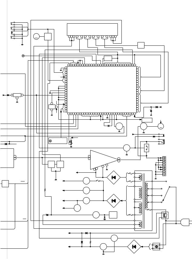
|
|
|
|
|
|
|
|
|
|
|
|
|
|
|
|
|
|
|
|
|
|
|
CD-C831W |
|
SWM3 |
|
|
|
|
|
|
|
|
|
|
|
|
|
|
|
|
|
|
|
|
|
|
L PROOF |
|
|
|
|
|
|
|
FL701 |
|
|
|
|
|
|
|
|
|
|
|
|
|
||
|
SWM4 |
|
|
|
|
|
|
|
|
|
|
|
|
|
|
|
|
|
|
|
|
||
|
F.A.S |
|
|
|
|
|
|
|
DISPLAY |
|
|
|
|
|
|
|
|
|
|
|
|
|
|
|
SOLM1 |
|
|
|
|
|
|
|
|
|
|
|
|
|
|
|
|
|
|
|
|
||
OLENOID |
|
M |
Q702 |
|
|
|
|
|
|
|
|
|
|
|
|
|
|
|
|
|
|
|
|
|
SWM5 |
|
|
|
1 2 3 |
4 ~ 15 |
16 ~ 25 |
26 ~ 28 |
29 ~ 36 37 38 39 |
|
|
|
|
|
|
|
|
|
|
|
|||
|
|
Q703 |
|
|
|
|
|
|
|
|
|
|
|
|
|
||||||||
|
CAM |
|
|
|
|
|
|
|
|
|
|
|
|
|
|
|
|
|
|
|
|
|
|
|
|
|
MM1 |
|
|
|
|
|
|
|
|
|
|
|
|
|
|
|
|
|
|
|
|
|
|
|
TAPE MOTOR |
|
|
|
|
|
|
|
|
|
|
|
|
|
|
|
Q705 |
|
|
|
|
|
|
|
|
|
|
|
|
|
|
|
|
|
|
|
|
|
|
|
Q706 |
|
|
|
|
|
|
|
|
|
|
|
|
|
|
|
|
|
|
|
|
|
|
|
Q707 |
|
|
|
|
|
|
|
SW601 |
|
|
|
|
|
|
|
|
|
|
|
|
|
|
|
|
|
|
|
|
|
|
|
SPAN |
|
|
|
|
|
|
|
|
|
|
|
|
|
|
|
|
|
|
|
|
|
|
SELECTOR |
|
|
|
|
|
|
|
|
|
|
|
|
|
|
|
|
|
|
|
|
|
|
|
|
|
|
|
|
|
|
|
|
|
D701 |
|
|
|
|
|
|
|
|
|
|
|
|
|
|
|
|
|
|
|
|
|
|
|
~D704 |
|
|
|
|
|
|
|
|
|
|
|
|
|
|
|
|
|
|
51 52 53 5455 5657 58 59 60 6162 63 64 65 66 67 68 69 70 71 72 73 7475 76 77 78 79 80 |
|
|
|
|
|
|||||||||||
|
|
|
|
|
|
50 |
|
|
|
|
|
|
|
|
|
|
|
|
81 |
|
|
|
|
|
|
|
|
|
|
49 |
|
|
|
|
|
|
|
|
|
|
|
|
82 |
|
|
|
|
|
|
|
|
|
|
48 |
|
|
|
|
|
|
|
|
|
|
|
|
83 |
|
|
|
|
|
|
|
|
|
+B7 |
47 |
|
|
|
|
|
|
|
|
|
|
|
|
84 |
|
|
|
|
|
|
|
|
|
46 VDD |
|
|
|
|
|
|
|
|
|
|
|
85 |
|
|
|
|
||
|
|
|
|
|
|
45 |
|
|
|
|
|
|
|
|
|
|
|
|
86 |
|
|
|
|
|
|
|
|
|
|
44 |
|
|
|
IC701 |
|
|
|
|
|
|
|
87 |
|
|
|
|
|
|
|
|
|
|
|
43 |
|
|
|
|
|
|
|
|
|
|
88 |
|
|
|
|
||
|
|
|
|
|
|
42 |
|
IX0281AW OR IX0310AW |
|
|
|
|
|
89 |
|
|
|
|
|||||
|
|
|
|
|
|
41 |
|
|
|
|
|
|
90 |
|
|
|
|
||||||
|
FM/AM |
|
|
|
|
|
|
SYSTEM CONTROL |
|
|
|
|
|
|
|
|
|
|
|||||
|
|
|
|
|
40 |
|
|
|
|
|
|
|
|
91 |
|
|
|
|
|||||
|
SWITCHING |
|
|
|
39 |
|
|
MICROCOMPUTER |
|
|
|
|
|
|
92 |
|
|
|
|
||||
7 |
|
IC704 |
|
|
|
|
|
|
|
|
|
|
|
|
|
|
|
||||||
1 |
3 |
|
|
38 |
|
|
|
|
|
|
|
|
|
|
|
|
93 |
|
|
|
|
||
|
KIA7042AP 2 |
|
|
|
37 |
|
|
|
|
|
|
|
|
|
|
|
|
94 |
|
|
|
|
|
|
|
|
+B7 |
36 |
|
|
|
|
|
|
|
|
|
|
|
|
95 |
|
|
|
|
||
|
RESET |
|
|
|
|
|
|
|
|
|
|
|
|
|
|
|
|
|
|
|
|||
|
|
|
|
1 |
|
35 |
|
|
|
|
|
|
|
|
|
|
|
|
96 |
|
|
|
|
|
|
|
|
|
34 |
AVDD |
|
|
|
|
|
|
|
|
|
|
|
97 |
|
|
|
|
|
|
|
|
|
|
|
|
|
|
|
|
|
|
|
|
|
|
|
|
|
|
|||
|
|
|
|
RX701 3 |
33 |
|
|
|
|
|
|
|
|
|
|
VDD |
98 |
|
UNSWITCH |
|
|||
|
|
|
|
2 |
|
32 |
|
|
|
|
|
|
|
|
|
|
99 |
|
+B7 |
|
|
||
|
|
|
|
|
31 |
|
|
|
VDD |
|
|
|
|
|
100 |
|
MEMORY |
|
|
||||
|
|
|
|
|
|
|
|
|
|
|
|
|
|
|
|
|
|||||||
|
|
|
|
|
+B7 |
|
30 29 28 2726 2524 23 22 21 2019 18 17 16 15 14 13 12 11 10 9 8 |
7 6 |
5 4 |
3 |
2 |
1 |
|
|
BACK UP |
|
|
||||||
|
|
|
|
|
|
|
|
|
|
|
|||||||||||||
|
|
|
|
|
|
|
|
|
|
|
|
|
|
|
|
|
|
|
TO CD |
+B5 |
|
|
|
|
|
|
|
|
|
|
|
|
|
+B7 |
|
|
|
|
|
|
|
SECTION |
|
|
|
||
|
|
|
|
|
|
|
|
|
|
|
|
|
|
|
|
|
|
|
|
|
|
||
|
|
|
|
|
|
|
|
|
|
|
|
XL701 |
Q704 |
|
|
|
|
Q960 |
|
M FANM901MOTOR |
|
||
|
|
|
|
|
|
|
|
|
|
|
|
4.19MHz |
|
|
|
|
|
|
|
|
|
|
|
|
|
|
|
|
|
|
|
|
|
|
|
|
|
|
+B5 |
|
|
|
|
|
|
||
|
|
|
|
KEY |
|
|
+B5 |
|
|
|
|
|
|
|
|
|
|
|
|
|
|
|
|
|
|
|
|
|
|
|
|
|
|
|
|
|
|
|
|
|
|
|
|
|
|
||
|
|
|
|
SW701~SW717 |
PHM1 |
|
|
|
|
|
|
|
|
|
|
|
|
|
|
|
|||
|
|
+B4 |
SW721~SW730 |
|
|
|
|
|
|
|
|
|
|
|
|
|
|
|
|||||
|
|
|
|
|
|
|
|
|
|
|
|
|
|
|
|
|
|
|
|||||
|
|
|
|
|
|
|
|
|
|
|
|
|
|
|
|
|
|
|
JK970 |
|
|
||
|
|
|
|
|
|
|
|
|
|
|
|
|
|
|
|
|
|
|
|
|
|
|
|
|
|
|
|
|
|
|
|
|
|
|
|
|
|
|
Q908 |
|
|
|
|
HEADPHONES |
|
||
|
|
|
|
|
|
|
|
|
|
|
|
|
|
|
|
|
|
RL901 |
|
|
|||
|
|
|
|
|
|
|
|
|
|
|
|
|
|
|
|
|
|
|
|
|
|
||
|
|
|
|
|
|
|
|
|
|
|
|
|
|
|
|
|
|
|
|
|
SO901 |
|
|
1 |
|
|
|
|
|
|
|
|
|
IC901 |
|
|
|
|
|
|
|
|
|
|
SPEAKER |
|
|
13 R |
|
|
|
|
|
|
14 |
|
|
|
FRONT |
|
|
|
|
|
TERMINAL |
|
|||||
|
|
|
|
|
|
|
|
|
|
|
|
|
|
|
|
|
|||||||
SP |
8 L |
|
|
|
|
|
|
10 |
STK407040B |
6 |
L-OUT |
|
|
|
|
|
|
SURROUND |
|
||||
CESSOR |
|
|
|
|
|
|
|
|
POWER AMP. |
7 R-OUT |
|
|
|
|
|
|
|
||||||
|
|
Q601 |
Q603 |
|
|
|
|
|
|
|
|
|
|
SPEAKER |
|
||||||||
|
|
|
|
|
|
|
|
+B |
|
|
|
|
|
|
|
|
|
|
|
|
|||
|
|
|
|
Q602 |
Q604 |
|
|
|
|
–B |
3 |
15 |
|
|
|
|
|
|
T801 |
|
|
|
|
|
|
|
|
|
|
|
|
|
|
|
|
|
|
|
|
|
POWER |
|
|
|
|
||
|
|
|
|
|
|
|
|
|
|
1 2 |
|
|
|
|
|
|
|
|
|
|
|
|
|
|
|
|
|
|
|
|
|
–15V |
|
|
D801 |
|
|
F802 |
|
TRANSFORMER |
|
FRONT |
|
||||
|
|
|
|
|
|
|
|
|
|
|
|
|
T4A L 250V |
|
|
|
SPEAKER |
|
|||||
|
|
|
|
|
|
|
–B1 |
|
|
|
|
|
|
|
|
|
|
|
|
|
|
|
|
|
|
|
|
|
|
|
|
VOLTAGE |
|
|
|
|
|
|
|
|
|
|
|
|
|
|
|
|
|
|
|
|
|
|
|
REGULATOR |
|
|
|
|
|
|
|
|
|
|
|
|
|
||
|
|
|
|
|
+B1 |
+7.3V |
|
Q822 |
|
|
|
|
|
|
|
|
|
|
|
230-240V |
SW801 |
|
|
|
Q121 |
|
REC |
|
|
|
|
F832 |
|
|
|
|
|
|
|
|
|
|
|
|
|||
|
|
|
|
|
|
|
|
|
|
|
|
F803 |
|
|
|
|
|
VOLTAGE |
|||||
|
Q122 |
|
|
|
|
|
|
|
|
T500mA L 250V |
|
|
T4A L 250V |
|
|
|
|
SELECTOR |
|||||
MUTING |
|
|
|
|
|
|
|
|
VOLTAGE |
|
|
|
|
|
|
|
|
|
|
220V |
|
|
|
|
|
|
+B4 |
+12V(ANALOG) |
REGULATOR |
|
|
|
|
|
|
|
|
|
|
|
|
||||||
|
|
|
|
|
|
|
|
|
|
|
|
|
|
|
|
|
|||||||
|
|
|
|
|
|
|
|
Q824 |
|
|
D803~D806 |
|
|
|
|
|
|
|
|
|
|
||
|
|
|
|
|
|
|
|
|
|
|
|
|
|
|
|
|
|
|
127V |
|
|
||
|
|
|
|
|
|
|
|
|
|
|
|
|
|
|
|
|
|
|
|
|
|
|
|
|
|
|
|
|
|
|
|
|
|
VOLTAGE |
|
|
|
|
|
|
|
|
|
|
|
|
|
|
|
|
|
|
+B5 |
+12V(MOTOR) |
Q823 REGULATOR |
|
|
|
|
|
|
|
|
|
110V |
|
|
||||
|
|
|
|
|
+B2 |
+5.6V |
Q821 |
|
VOLTAGE |
|
|
|
|
|
|
|
|
|
T.F |
|
|
|
|
|
|
|
|
|
|
|
|
|
|
|
|
|
|
|
|
|
|
|
|
||||
|
|
|
|
|
|
|
|
|
REGULATOR |
|
|
|
|
|
|
|
|
|
|
|
|
||
|
|
|
|
ZD801 |
|
|
|
|
|
Q801 |
|
D807 |
|
|
|
|
|
|
|
|
|
|
|
|
|
|
|
|
|
|
|
|
|
|
|
|
|
|
|
|
|
|
|
RL801 |
AC POWER |
||
|
|
|
|
|
|
|
|
|
|
|
~D809 |
|
|
F805 |
|
|
|
|
|
||||
|
|
|
|
|
|
|
|
|
|
|
|
|
|
|
|
|
|
|
|||||
|
|
|
|
|
|
|
|
|
|
|
|
|
|
|
|
|
|
|
|
|
SUPPLY CORD |
||
|
|
|
T1/T2 |
|
|
|
|
|
|
|
|
ZD802 |
|
T2A L 250V |
|
|
|
|
|
|
|||
|
|
|
|
|
|
|
|
|
|
|
|
|
|
|
|
|
|
|
|
|
|
|
|
|
|
|
|
|
|
|
|
|
|
|
|
|
|
|
|
|
|
|
|
|
|
AC 110/127/220/230-240V |
|
|
|
|
|
|
|
|
|
|
|
|
|
|
|
|
|
|
|
|
|
|
|
|
50/60Hz |
|
|
|
|
|
|
+B6 |
+5V |
|
|
|
|
|
|
|
|
|
|
|
|
|
|
|
|
|
|
|
|
|
|
|
|
|
|
|
|
|
|
|
|
|
|
|
|
|
|
|
|
|
|
|
|
|
|
|
|
|
|
|
|
Q802 |
|
|
|
|
|
|
|
|
|
|
|
|
|
|
|
|
|
+B7 |
UNSWITCH |
|
Q803 |
|
|
|
|
|
|
|
|
|
|
|
|||
|
|
|
BAIS |
|
|
|
|
|
|
|
|
|
|
|
|
|
|
|
|
||||
|
|
|
|
|
|
|
|
|
|
|
|
|
|
|
|
|
|
|
|
|
T802 |
|
|
|
|
|
|
|
|
|
|
|
|
|
|
|
|
|
|
|
|
|
|
|
POWER |
|
|
|
|
|
|
|
|
|
|
|
|
|
|
|
|
|
|
D810~D813 |
TRANSFORMER |
|
|
||||
Figure 15 BLOCK DIAGRAM (3/3)
– 15 –

CD-C831W
A
B
C
D
E
F
G
H
|
|
|
|
|
|
|
|
|
|
FM SIGNAL |
|
|
PLAYBACK SIGNAL |
|
|
|
|
RECORD SIGNAL |
|
|
|||||||||||||||||||||||||
|
|
|
|
|
|
|
|
|
+B |
|
|
|
|
|
|
|
|
|
|
|
|
|
|
|
|
|
|
|
|
|
|
|
|
|
|
|
|
|
|
|
|
|
|
|
|
|
PWB |
|
1 |
|
|
|
BI6011 |
|
|
|
|
|
|
|
|
|
|
|
|
|
|
|
|
|
|
|
|
|
|
|
|
|
|
|
|
|
|
|
|
|
|
|
|
|
|
|
|
|
CNS11 |
|
|
|
|
|
|
|
|
|
|
|
|
|
|
|
|
|
|
|
|
|
|
|
|
|
|
|
|
|
|
|
|
|
|
|
|
|
|
|
|
|
|
|
|
|
|
R-CH |
|
|
|
|
|
|
|
|
|
|
|
|
|
|
|
|
|
|
|
|
|
|
|
|
|
|
|
|
|
|
|
|
|
|
|
|
|
|
|
|
|
12P23- C |
SERVOCDTO |
|
2 |
A_GND |
|
|
|
2 |
|
|
|
|
|
|
|
|
|
|
|
|
|
|
|
|
|
|
|
|
|
|
|
|
|
|
|
|
|
|
|
|
|
|
|
|
|
CNP11 |
L-CH |
|
|
|
|
|
R615 3.9K |
0.001 |
R645 100K |
|
|
|
|
2.2K |
|
|
|
|
R609 2.2K |
|
|
|
|
|
IC601 |
M62439SP |
|
PROCESSORAUDIO |
|
10K |
|
R612 22K |
|||||||||||||
3 |
|
|
|
3 |
|
|
|
|
|
|
|
|
|
|
|
|
|
|
|
|
|
|
|||||||||||||||||||||||
|
|
|
|
|
|
|
|
|
|
|
|
|
|
|
|
|
|
|
|
|
|
|
|
|
|
|
|
|
|
|
|
|
|
|
|
|
|
|
|
|
|
|
|||
|
|
|
CD_GND |
|
|
|
|
|
|
|
|
|
|
|
|
|
|
|
|
|
|
|
C601 |
|
|
R639 |
|
|
|
|
|
|
|
|
|
|
|
|
|
|
|
|
|||
|
|
|
4 |
|
|
|
4 |
|
|
|
|
|
|
|
|
|
|
|
|
|
|
|
|
|
|
|
|
|
|
|
|
|
|
|
|
|
|
|
|
|
|
||||
|
|
|
+7V |
|
|
|
+B |
|
|
|
|
|
|
|
|
|
|
|
|
|
|
|
4.7/50 |
|
|
47K |
|
|
|
|
|
|
|
|
|
|
|
|
|
|
|
|
|
||
|
|
|
5 |
|
|
|
5 |
|
|
|
|
|
|
|
|
|
|
|
|
|
|
|
|
|
|
|
1 |
|
|
|
|
|
|
|
|
20 |
|
|
|
|
|
||||
|
|
|
|
|
|
|
|
|
|
|
|
|
|
|
|
|
|
|
|
|
|
|
|
|
|
|
|
|
|
|
|
|
|
|
|
|
|
|
|
||||||
|
|
|
|
|
|
|
|
|
|
|
|
|
|
|
|
|
|
|
|
|
|
|
|
|
|
|
|
|
|
|
|
|
|
|
|
|
|
|
|
|
|
||||
|
|
|
6 |
+12V |
|
|
|
6 |
+B |
|
|
|
|
|
|
|
|
|
|
|
|
|
|
|
C605 |
R607 |
1.5K |
|
2 |
|
|
|
|
|
|
|
|
19 R608 |
|
1. |
|||||
|
|
|
|
|
|
|
|
|
|
|
|
|
|
|
|
|
|
|
|
|
|
|
|
R605 |
1.5K |
|
3 |
|
|
|
|
|
|
|
|
18 R606 |
|
1. |
|||||||
|
|
|
|
|
|
|
|
|
|
|
|
|
|
|
|
|
|
|
|
|
|
|
|
|
|
|
|
|
|
|
|
|
|
|
|||||||||||
|
|
|
|
|
|
|
|
|
|
|
|
|
|
|
|
|
|
|
|
|
|
|
|
|
4.7/50 |
R603 |
1.5K |
|
4 |
|
|
|
|
|
|
|
|
17 |
R604 |
|
1. |
||||
|
|
|
|
|
|
|
|
|
|
|
|
|
|
|
|
|
|
|
|
|
|
|
|
|
|
|
|
|
|
|
|
|
|
|
|
|
|
|
|
|
|
|
|
||
|
|
|
|
|
|
|
|
|
|
|
|
|
|
|
|
|
|
|
|
|
|
|
|
C603 |
R601 |
1.5K |
|
5 |
|
|
|
|
|
|
|
|
16 R602 |
|
1. |
||||||
|
|
|
|
|
|
|
|
|
|
|
|
|
|
|
|
|
|
|
|
|
|
|
|
4.7/50 |
C611 |
0.033 6 |
|
|
|
|
|
|
|
|
15 |
|
C612 |
|
0 |
||||||
|
|
|
|
|
|
|
|
|
|
|
|
|
|
|
|
|
|
|
|
|
|
|
|
|
|
|
|
|
|
|
|
|
|
|
|
||||||||||
|
|
|
|
|
|
|
|
|
|
|
|
|
|
|
|
|
|
|
|
|
|
|
|
|
|
C615 |
|
C613 |
7 |
|
|
|
|
|
|
|
|
14 |
|
C614 |
|
0 |
|||
|
|
|
|
|
|
|
|
|
|
R635 |
|
R621 |
C635 |
|
|
R613 |
|
R611 |
0.22 |
|
0.22 |
|
|
|
|
|
|
|
|
|
|
|
|
|
|
||||||||||
|
|
|
|
|
|
|
|
|
|
|
|
|
|
|
|
|
|
|
8 |
|
|
|
|
|
|
|
|
13 |
|
|
|
|
|
||||||||||||
|
|
|
|
|
|
|
|
|
|
330 |
|
10K |
|
0.0047 |
|
|
10K |
|
|
330 |
|
|
|
|
|
|
|
|
|
|
|
|
|
|
|
|
|
|
|
||||||
|
|
|
|
|
|
|
|
|
|
|
|
|
|
|
|
|
|
|
|
|
C621 |
|
|
|
|
|
|
|
9 |
|
|
|
|
|
|
|
|
12 |
|
|
|
|
|
||
|
|
|
|
|
|
|
|
|
|
|
|
Q603 |
|
|
|
|
|
|
|
|
|
|
|
|
|
|
|
10 |
|
|
|
|
|
|
|
|
11 |
|
|
|
|
|
|||
|
|
|
|
|
|
|
|
|
|
|
|
|
|
|
Q601 |
|
|
0.1/50 |
|
|
|
|
|
|
|
|
|
|
|
|
|
|
|
|
|
|
|
|
|||||||
|
|
|
|
|
|
|
|
|
|
|
|
2SC3331 |
|
|
|
|
|
|
|
|
C617 |
|
|
|
|
|
|
|
|
|
|
R610 |
|
|
|
||||||||||
|
|
|
|
|
|
|
|
|
|
|
|
|
|
|
2SC3331 R617 |
|
|
|
|
|
|
|
|
|
|
|
|
|
|
|
|
|
|
|
|||||||||||
|
|
|
|
|
|
|
|
|
|
|
|
C625 |
|
|
|
|
|
|
|
|
|
10/50 |
|
|
|
|
|
|
|
|
|
|
|
|
|
||||||||||
|
|
|
|
|
|
|
|
|
|
|
|
R619 |
|
|
|
|
C623 |
|
|
|
|
|
|
|
C619 |
|
|
|
|
|
R623 |
|
|
|
|
|
|
|
|
||||||
|
|
|
|
|
|
|
|
|
|
|
|
2.2K |
|
|
|
|
0.001 |
|
|
|
|
|
|
|
|
|
|
|
|
|
|
|
|
|
|
|
|
||||||||
|
|
|
|
|
|
|
|
|
|
|
|
|
|
|
|
|
|
|
|
|
|
|
|
|
|
|
|
10K |
|
|
|
|
|
|
|
|
|||||||||
|
|
|
|
|
|
|
|
|
|
|
|
R620 |
100K |
|
|
|
C624 |
|
|
|
|
|
|
|
0.022 |
|
|
ZD601 |
|
|
|
|
|
|
|
|
|||||||||
|
|
|
|
|
|
|
|
|
|
|
|
2.2K |
|
|
|
0.001 |
R618 |
|
|
|
|
|
|
|
|
|
|
|
|
|
|
|
|
|
|
|
|
||||||||
|
|
|
|
|
|
|
|
|
|
|
|
C626 |
|
|
|
|
|
|
|
|
|
|
|
|
|
|
MTZJ2.4B |
|
|
|
|
|
|
|
|
|
|||||||||
|
|
|
|
|
|
|
|
|
|
|
R616 3.9K |
|
|
|
|
Q602 |
|
2.2K |
|
|
|
|
|
|
|
|
|
|
|
|
|
|
|
|
|
|
|
|
|
|
|
||||
|
|
|
|
|
|
|
|
|
|
|
0.001 |
|
R646 |
|
|
|
|
|
|
|
|
|
|
|
|
|
|
|
|
|
|
|
|
|
|
|
|
|
|
|
|
|
|||
|
|
|
|
|
|
|
|
|
CD_+B |
R636 |
|
|
C634 |
|
|
|
R614 |
0.1/50 |
|
|
|
|
|
|
|
|
|
|
|
|
|
|
|
|
|
|
|
|
|||||||
|
|
|
|
|
|
|
|
|
2SC3331 |
|
|
|
|
|
|
|
|
|
|
|
|
|
|
|
|
|
|
|
|
|
|
|
|
|
|||||||||||
|
|
|
|
|
|
|
|
|
|
|
|
Q604 |
|
|
|
2SC3331 |
|
|
|
|
|
|
C622 |
|
|
|
|
|
R629 |
|
|
|
|
|
|
|
|
|
|
|
|
|
|||
|
|
|
|
|
|
|
|
12 |
|
330 |
|
|
|
|
|
0.0047 |
|
|
|
10K |
|
|
|
|
|
|
|
330(1/2W) |
|
|
|
|
|
|
|
|
|
||||||||
|
|
|
|
|
|
|
|
|
CD_GND |
|
|
R622 |
|
|
|
|
|
|
|
|
|
|
|
|
|
|
|
|
|
|
|
|
|
|
|
|
|
|
|
|
|
|
|
|
|
|
|
|
|
|
|
|
SECTION |
13 |
|
|
10K |
|
|
|
|
|
|
|
|
|
|
|
|
|
|
|
|
|
|
|
|
|
|
|
|
|
|
|
|
|
|
|
|
|
|
|
|
|
|
|
|
E- |
|
|
|
|
|
|
|
|
|
|
|
|
R628 22K |
|
|
|
|
|
|
|
|
|
|
|
|
|
|
|
|
|
|
|
|
|
|
||||
|
|
|
|
|
|
1 |
L |
|
|
C627 |
|
R625 |
|
C629 |
|
|
|
|
|
|
|
|
+B |
|
|
|
|
|
|
|
|
|
|
|
|
|
|||||||||
|
|
|
|
|
|
|
|
|
|
|
|
|
|
|
|
|
|
|
|
|
|
|
|
|
|
|
|
|
|
|
|
|
|
|
|||||||||||
|
|
|
|
|
|
|
|
|
|
|
|
|
|
|
|
|
|
|
|
|
|
|
|
|
|
|
|
|
|
|
|
|
|
|
|
|
|
||||||||
|
|
|
|
|
|
|
|
|
A_GND |
|
|
22/25 |
|
22K |
|
|
22/25 |
|
|
|
|
|
|
|
|
|
|
|
|
|
|
|
|
|
|
|
|
|
|
|
|
|
|||
|
|
|
|
|
|
|
|
2 |
|
|
|
|
|
|
|
|
|
|
|
|
|
|
|
|
|
|
|
|
|
|
|
|
|
|
|
|
|
|
|
|
|
|
|
|
|
|
|
|
|
|
|
P181 |
POWER |
|
|
|
|
|
|
|
|
|
|
|
|
|
|
|
|
|
|
|
|
|
|
|
|
|
|
|
|
|
|
|
|
|
|
|
|
|
|
|
|
|
|
|
|
3 |
R |
|
|
|
|
|
|
|
|
|
|
|
|
|
|
|
|
|
|
|
|
|
|
|
|
|
|
|
|
|
|
|
|
|
|
|
|
||
|
|
|
|
|
|
|
|
|
|
|
|
|
|
|
|
|
|
|
|
|
|
|
|
|
|
|
|
|
|
|
|
|
|
|
|
|
|
|
|
|
|
|
|
|
|
|
|
|
|
|
|
|
|
10 |
A_12V |
+B |
|
|
|
|
|
|
|
|
|
|
|
|
|
|
|
|
|
+B |
|
|
|
|
|
|
|
|
|
|
|
|
|
|
|
|
|
|
|
|
|
|
|
|
|
|
|
|
|
|
|
|
|
|
|
|
|
|
|
|
|
R155 |
|
|
|
|
|
|
|
|
|
|
R175 |
|
|
|
|
|
|||||
|
|
|
|
|
|
|
TO |
|
|
|
|
|
|
|
|
|
|
|
|
|
|
|
|
|
|
|
|
|
|
|
|
|
|
|
|
|
|
|
|
||||||
|
|
|
|
|
|
|
2 |
A_GND |
|
|
|
|
|
|
|
|
|
|
|
|
|
|
|
150 |
|
|
|
|
|
|
|
|
|
|
|
1K |
|
|
|
|
|
|
|
||
|
|
|
|
|
|
|
|
|
|
|
|
|
|
|
|
|
|
|
|
|
|
|
|
|
|
|
|
|
|
|
|
|
|
|
|
|
|
|
|
|
|||||
|
|
|
|
|
|
|
|
|
|
|
|
|
|
|
|
|
|
|
|
|
|
|
|
|
|
|
|
|
|
|
|
|
|
|
|
|
|
|
|
|
|
|
|
|
|
|
|
|
|
|
|
|
|
14 |
M_GND |
|
Q109 ~ Q111: SWITCHING |
|
|
|
|
|
|
|
|
|
|
|
|
|
|
|
|
|
|
|
|
|
|
|
|
|
|
|
|
|
|
|
|||
|
|
|
|
|
|
|
|
|
|
|
|
|
|
|
|
Q110 |
|
|
|
|
|
|
|
|
|
|
|
|
|
|
|
|
|
|
|
|
|
|
|||||||
|
|
|
|
|
|
|
|
|
|
|
|
|
|
C109 |
|
R114 |
|
KRC104 M |
|
|
|
|
R173 |
|
|
|
|
|
|
|
R174 |
|
|
|
|
|
|||||||||
|
|
|
|
|
|
|
|
|
|
|
|
|
|
0.047 |
|
10K |
|
0V |
|
3.4V |
|
|
|
5.6K |
|
|
|
|
|
|
|
|
5.6K |
|
|
|
|
|
|||||||
|
|
|
|
|
|
|
|
|
|
|
|
|
|
R113 |
|
|
|
|
2 |
|
|
3 |
|
C153 |
|
|
|
|
|
|
|
|
|
|
|
|
|
|
|
|
|
|
|
||
|
|
|
|
|
|
|
|
|
|
|
|
|
|
|
|
|
|
|
1 |
|
|
|
|
|
|
|
|
|
|
|
|
|
|
|
|
|
|
|
|
|
|
||||
|
|
|
|
|
|
|
|
|
|
|
|
|
|
10K |
|
|
R115 |
|
|
|
|
|
100/16 |
|
R171 |
|
|
Q114 |
2SC3331 |
|
|
R172 |
|
|
|
|
|
||||||||
|
|
|
|
|
|
|
|
|
|
|
|
|
|
8.6V |
|
|
0V |
|
|
3.4V |
|
|
|
|
|
|
|
|
|
|
|||||||||||||||
|
|
|
|
|
|
|
|
|
|
|
|
9.3V |
|
|
|
4.7K |
|
|
1 |
|
Q113 |
|
220K |
|
|
|
|
|
220K |
|
|
|
|
|
|||||||||||
|
|
|
|
|
|
|
|
|
|
|
|
|
|
|
|
|
|
|
|
|
|
|
|
|
|
|
|
|
|
|
|
|
|
|
|
||||||||||
|
|
|
|
|
|
|
|
|
|
|
|
|
|
|
|
|
|
|
|
|
|
|
|
|
|
|
|
|
|
|
|
|
|
|
|
|
|
|
|
|
|
||||
|
|
|
|
|
|
|
CNP101 |
|
|
|
|
|
|
|
|
|
|
|
|
|
3 |
|
|
|
C155 3.3/50 |
|
|
|
R132 |
33K |
3.3/50 |
|
|
R136 |
8.2K |
C154 |
|||||||||
|
|
|
|
|
|
|
|
|
|
|
|
|
|
|
|
|
|
0V |
|
|
2SC3331 |
|
|
|
|
|
|
|
|||||||||||||||||
|
R-CH |
|
|
CNS101 |
|
|
|
|
|
|
|
|
Q109 |
|
|
|
|
2 |
|
|
Q111 |
|
R169 |
|
R120 |
|
|
R170 |
|
C156 |
|
|
|
|
|
|
|
|
|||||||
|
|
|
|
|
|
|
|
|
|
|
|
9.3V |
|
2SA1318 |
|
|
|
|
|
KRC104 M |
|
|
|
|
|
|
|
|
|
|
|
|
|
|
|
||||||||||
|
|
|
|
|
|
|
|
|
|
|
|
|
|
|
|
|
|
680 |
|
|
|
|
|
680 |
|
|
|
|
|
|
|
|
|
|
|
||||||||||
|
|
TAPE1 |
|
|
|
|
|
|
|
|
|
|
|
|
|
|
|
|
|
|
|
|
|
|
|
|
|
|
|
|
|
|
|
|
|
|
|
|
|
|
|||||
|
|
|
|
|
|
|
|
|
|
|
|
|
|
|
|
|
|
|
R112 |
|
|
|
|
|
|
|
|
|
|
|
|
|
|
|
|
|
|
|
|
|
|
|
|||
|
PLAYBACK HEAD |
|
|
|
|
|
|
|
|
|
|
|
|
|
|
|
|
|
|
|
|
|
|
|
|
|
|
|
|
|
|
|
|
|
|
|
|
|
|
|
|||||
|
|
|
|
|
|
|
|
|
|
|
|
|
|
|
|
|
10K |
|
|
|
|
|
|
|
|
|
|
|
|
|
|
|
|
|
|
|
|
|
|
|
|||||
|
|
|
|
|
1 |
TAPE1_R |
1 |
|
|
C102 |
|
|
|
|
|
|
|
|
|
R102 |
|
|
|
|
|
56 |
|
|
|
C120 |
|
|
|
|
|
|
|
|
|
|
|
||||
|
|
|
|
|
|
|
0.001 |
|
|
|
|
|
|
|
|
|
1K |
|
|
|
|
|
|
C118 |
|
|
|
560P |
|
|
|
|
|
|
|
|
|
|
|
||||||
|
|
|
|
|
2 |
A_GND |
2 |
|
|
|
|
|
|
|
|
|
|
|
|
|
|
|
|
|
|
|
|
|
|
|
|
|
|
|
|
|
|
|
|||||||
|
|
|
|
|
|
|
C101 |
|
|
|
|
|
|
|
|
|
|
|
|
|
|
|
|
0.033 |
|
|
|
|
|
|
R126 |
|
|
|
|
|
|||||||||
|
|
|
|
|
3 |
TAPE1_L |
3 |
|
|
|
|
|
|
|
|
|
|
|
|
|
|
|
|
|
|
R122 |
|
|
|
|
|
|
|
|
|
|
|
||||||||
|
|
|
|
|
|
|
0.001 |
|
|
|
|
|
|
|
|
|
1K |
|
|
|
|
|
|
100K |
|
|
R124 3.9K |
|
5.6K |
|
|
|
R134 |
68K |
|
R138 |
|||||||||
|
L-CH |
|
|
|
|
|
|
|
|
|
|
|
|
|
|
|
|
|
|
|
|
|
|
|
C116 |
|
|
|
|
|
|
|
|
|
|
|
|||||||||
|
|
|
|
|
|
|
|
|
|
|
|
|
|
|
|
|
|
|
|
|
R101 |
|
|
|
|
47/25 |
|
|
|
|
|
|
|
|
|
|
|
|
|
|
|
|
|
||
|
|
|
|
|
|
|
|
|
|
|
|
Q104 2SC2389SE |
|
|
|
|
|
|
|
|
|
|
|
|
|
R118 |
|
|
|
|
|
|
|
|
|
|
|
|
|
|
|
|
|
|
|
|
PLAYBACK HEAD |
CNS102 |
|
CNP102 |
|
|
|
0V |
2.2K |
|
|
R108 |
47K |
0V |
|
|
0.001 |
|
|
1K |
|
23 |
C114 |
|
21 |
C122 |
|
19 |
|
|
|||||||||||||||
|
|
|
|
|
0V |
|
|
|
|
|
330P 24 |
|
22 |
|
|
|
|
|
20 |
|
|
|
|
|
|||||||||||||||||||||
|
|
|
TAPE2 |
|
|
|
|
|
|
|
C106 |
|
|
0.7V |
|
|
|
|
|
|
|
|
|
|
|
|
|
330P |
|
|
|
1/50 |
|
|
|
|
|
|
|
||||||
|
|
RECORD/ |
|
|
|
|
|
|
|
180P |
|
|
|
R104 |
|
|
|
|
|
0V |
|
|
|
C112 |
|
|
|
|
|
|
|
|
|
|
|
|
|
|
|
|
|
|
|
||
|
|
|
|
|
|
|
|
|
|
|
|
|
|
|
|
|
|
|
|
|
|
|
|
|
|
|
|
|
|
|
|
|
|
|
|
|
|
|
|
|
|
|
|
|
|
ERASE |
|
|
1 |
M_GND |
1 |
|
|
|
|
|
|
R106 |
|
|
|
|
|
|
|
|
|
|
|
|
|
|
– |
|
|
|
|
|
|
|
|
|
|
|
|
|
|
||||
|
|
|
|
|
|
|
|
3.3K |
|
|
|
|
|
|
|
|
|
|
|
|
|
|
|
112K |
|
|
|
|
|
|
|
|
|
|
|
||||||||||
|
|
|
|
|
|
|
|
|
|
|
|
|
|
|
|
|
|
|
C108 |
|
|
|
|
|
|
|
+ |
|
|
|
|
|
|
|
|
|
|
|
|||||||
HEAD |
|
|
2 |
ERASE |
2 |
|
|
|
0V |
|
0.7V |
|
|
R110 |
4.7K |
|
0V |
2SC3331 |
|
|
|
|
|
|
|
Hich=T1 |
|
|
|
|
|
|
|
|
|
|
|
|
|
||||||
|
|
|
|
|
3 |
TAPE2_R2 |
3 |
|
|
|
|
|
|
|
Q108 |
|
|
|
|
|
|
+ |
112K |
|
|
|
|
|
|
|
|
|
|
|
|||||||||||
|
R-CH |
|
|
|
|
|
|
|
Q106 |
|
|
|
|
|
|
|
|
|
|
|
|
|
|
– |
|
|
|
|
|
|
|
|
|
|
|
|
|
|
|||||||
|
|
|
4 |
A_GND |
4 |
|
|
|
2SC2389 SE |
|
|
|
|
|
|
|
|
|
1 |
|
2 |
3 |
|
|
|
|
4 |
|
5 |
|
|
|
6 |
|
|
||||||||||
|
|
|
|
|
|
|
|
|
|
|
|
|
|
|
|
|
|
|
|
|
|
|
|
|
|
|
|
|
|
|
|
|
|||||||||||||
|
|
|
|
|
5 |
TAPE2_R1 |
5 |
|
|
|
|
|
|
|
|
|
|
|
|
|
|
|
|
C111 |
|
|
|
|
|
|
|
|
|
|
|
|
|
|
|
|
C128 3.3/50 R137 |
||||
|
|
|
|
|
|
|
|
0V 2SC2389 SE |
|
R107R109 47K4.7K |
|
Q107 |
2SC3331 |
C107 0.001 |
|
330P |
|
|
|
|
|
|
|
33K |
|
|
C127 0.022 |
||||||||||||||||||
|
|
|
|
|
6 |
TAPE2_L1 6 |
|
|
|
|
|
|
|
|
|
|
|
|
|
|
|
||||||||||||||||||||||||
|
|
|
|
|
|
|
|
|
|
|
|
|
|
|
|
|
|
|
|
|
|
|
|
|
|
|
|
|
|
|
|
|
|
|
|
|
|
|
|
||||||
|
L-CH |
|
|
|
|
|
|
|
|
|
|
|
|
|
|
|
|
|
|
|
R117 |
|
C113 |
|
|
|
|
|
|
|
|
|
|
|
|
|
|
|
|
||||||
|
|
|
7 |
TAPE2_L2 |
7 |
|
|
|
|
|
Q105 |
|
|
|
|
|
|
|
|
|
|
|
|
|
|
|
|
|
|
|
|
|
|
|
|
|
|
|
|||||||
|
|
|
|
|
|
|
|
0V |
|
|
|
|
|
|
|
|
|
|
|
1K |
|
330P |
|
|
|
|
|
C121 |
|
|
|
|
|
|
|||||||||||
|
|
|
|
|
|
|
|
|
|
|
|
2SC2389 SE |
|
|
|
|
|
|
|
|
|
|
|
C115 |
|
|
|
R123 3.9K |
|
|
|
|
|
|
|
||||||||||
|
|
|
|
|
|
|
|
|
|
|
|
|
|
|
0.7V |
|
|
|
|
0V |
|
|
|
|
|
|
|
|
|
|
1/50 |
|
|
|
|
|
|
|
|||||||
|
|
|
|
|
|
|
|
|
|
|
|
|
|
|
|
|
|
|
|
|
|
|
|
|
|
47/25 |
|
|
|
|
|
|
|
|
|
|
|
|
|
|
|
|
|
||
|
|
|
|
|
|
|
|
|
|
|
C105 |
|
|
|
R105 |
|
|
|
0V |
|
|
|
|
|
|
|
|
R121 |
|
|
|
|
|
|
R125 |
|
|
|
|
|
|
|
|||
|
|
|
|
|
|
|
|
|
|
|
180P |
0V |
|
|
3.3K |
0.7V |
|
|
|
|
|
|
|
|
|
|
100K |
|
|
|
|
|
|
5.6K |
|
|
|
|
|
|
|
|
|||
|
|
|
|
|
|
|
|
|
|
|
|
|
|
|
|
|
|
|
|
|
|
C117 |
|
|
|
|
|
|
|
|
|
|
|
|
|
|
|||||||||
|
|
|
|
|
|
|
|
|
|
|
|
|
|
|
R103 |
|
|
0V |
|
|
|
|
|
|
|
|
|
|
|
|
|
|
|
|
|
|
|
|
|
|
|
||||
|
|
|
|
|
|
|
|
|
|
|
|
|
|
|
2.2K |
|
|
|
|
|
|
|
|
|
|
0.033 |
|
|
|
C119 |
|
|
|
|
|
|
|
|
|
|
|
||||
|
|
|
|
|
|
|
|
|
|
|
|
|
|
|
|
|
|
|
|
|
|
|
|
|
|
|
|
R119 |
|
|
|
|
|
|
|
|
|
|
|
|
|
||||
|
|
|
|
|
|
|
|
|
|
|
|
|
|
|
|
|
|
|
|
|
|
|
|
|
|
|
|
|
|
560PR131 |
|
|
|
|
|
|
|
|
|||||||
|
|
|
|
|
|
|
|
|
|
|
|
|
|
Q103 |
|
|
|
|
|
|
|
|
|
|
|
|
56 |
|
|
|
|
|
|
|
|
|
|
|
|||||||
|
|
|
|
|
|
|
|
|
|
|
|
|
Q103 ~ Q108: SWITCHING |
|
|
|
|
|
|
|
|
|
|
|
|
|
|
|
|
|
|
|
|
|
|
|
R135 |
||||||||
|
|
|
|
|
|
|
|
|
|
|
|
|
|
|
|
|
|
R111 |
|
|
|
|
|
|
|
|
|
|
|
|
|
|
|
|
8.2K |
||||||||||
|
|
|
|
|
|
|
|
|
|
|
|
|
|
|
|
|
|
|
|
|
|
|
|
|
|
|
|
|
|
|
|
|
|
|
|
|
|
|
|
|
|
|
|
||
|
|
|
|
|
|
|
|
|
|
|
|
|
|
|
|
|
|
|
|
|
|
|
|
|
10K |
|
|
|
|
|
|
|
|
|
|
|
|
|
|
|
|
|
|
|
|
• NOTES ON SCHEMATIC DIAGRAM can be found on page 12.
1 |
2 |
3 |
4 |
5 |
6 |
Figure 16 SCHEMATIC DIAGRAM (1/9)
– 16 –

CD-C831W
L |
CD SIGNAL |
|
|
C602 |
|
|
R642 |
|
|
|
|
|
608 |
1.5K |
4.7/50 |
|
|
|
|
|
|
|
|
|
|
|
47K |
|
|
|
|
|
||
606 |
1.5K |
C606 |
|
|
|
|
|
C654 |
|
|
|
|
|
|
|
|
|
||||
604 |
1.5K |
4.7/50 |
|
R640 47K |
|
|
|
4.7/50 |
|
|
|
|
|
|
|
|
|
||||
602 |
1.5K |
|
|
|
|
|
|
|
|
|
612 |
0.033 |
C604 |
(1/2W)330 |
330 |
|
|
C653 |
4.7/50 |
|
C652 |
R612 |
22K |
R630 |
|
|
|
|||||
614 |
0.22 |
4.7/50 |
|
R626 |
2.2K |
R641 |
|
|
|
|
|
|
|
|
|
|
47K |
|
|
|
|
|
|
–B |
|
C628 |
|
|
Q651 |
|
||
|
|
|
|
0.22 |
|
|
2SC3331 |
|
||
|
|
|
|
|
|
|
|
|
||
|
|
|
|
R624 |
|
|
|
|
R651 |
|
|
|
|
|
|
|
|
|
680 |
|
|
|
|
|
|
|
|
|
|
|
|
|
|
|
|
|
|
|
|
R653 |
C651 |
1/50 |
|
|
C616 10P |
C620 10/50 C618 0.022 ZD602 MTZJ2.4B |
|
|
|
R638 |
220K |
R656 1K |
|
|
|
|
|
|
|
|
|
|
3.3/50 |
|
|
|
|
|
|
|
|
220K |
R655 |
|
|
|
|
|
|
|
|
|
|
5.6K |
|
|
|
|
|
|
|
|
|
R637 |
|
|
|
|
|
|
|
|
|
|
220K |
|
|
|
|
|
|
–B |
|
|
|
|
|
|
|
|
|
|
|
|
|
+B |
|
|
|
+B |
|
|
|
|
|
MUTING |
|
|
|
|
|
REC_R |
|
L |
|
|
|
|
|
||||
|
|
|
|
|
Q122 |
R156 |
|
|
|
|
|
|
REC |
|
|
|
|
|
|||
|
|
|
|
|
220K |
|
|
|
|
|
|
|
|
|
|
|
|||||
|
|
|
|
2SC3331 |
|
|
R153 |
|
|
|
|
|
|
|
|||||||
|
|
|
|
0V |
|
|
R154 |
|
|
|
0V |
R157 |
|
|
|
|
|
||||
|
|
C154 47/16 |
|
|
|
|
10K |
|
|
10K |
|
|
220K |
|
|
|
|
|
|||
|
|
|
|
|
0.7V |
R146 10K |
|
|
0.7V |
|
|
|
|
|
|
|
|||||
|
|
|
|
0V |
|
|
|
|
|
|
|
Q121 |
0V |
|
|
|
|
|
|
||
|
|
|
|
|
|
|
|
|
|
|
|
|
2SC3331 |
|
|
|
|
|
|
|
|
|
|
|
|
|
|
|
|
|
|
|
|
|
MUTING |
|
|
|
|
|
|
|
|
|
R136 8.2K |
|
|
C130 |
470P |
560 |
R142 56 |
C140 |
0.0033 |
|
|
|
|
|
|
|
|
|
|
|
|
R134 |
68K |
R138 |
6.8K |
C132 0.001 |
R140 |
C136 |
0.068 |
C142 |
1/50 |
C145 |
22/25 |
C146 |
220/10 |
|
|
|
|
|
|
|
|
|
|
|
|
|
|
|
C134 |
|
|
|
|
|
|
|
|
R158 |
|
+B |
|
|
|
|
|
|
|
|
|
|
22/25 |
|
|
|
|
|
|
|
|
220 |
|
|
|
||
6 |
|
|
7 |
|
8 |
|
9 |
10 |
11 |
|
12 |
|
ANDPLAYBACK RECORD/PLAYBACKAMP. |
SWITCHING Q124 2SA1015GR |
|
R164 4.7K |
R162 |
3 |
|||
|
|
|
|
|
|
|
2 |
||||||||||||||
19 |
|
18 |
|
17 |
|
16 |
15 |
14 |
|
13 |
|
|
11.7V |
47K |
|
||||||
|
|
|
|
|
|
|
– |
56K |
|
Nor/CrO2 |
RIPPLE |
|
Vcc |
|
|
|
|
|
|
||
|
|
|
|
|
|
|
+ |
|
|
|
|
|
|
|
|
|
11.6V |
|
|||
|
C128 3.3/50 R137 6.8K |
C131 470P 0.001 |
560 |
0.068 |
56 |
0.0033 |
|
|
|
|
|
IC101 AN7345K |
|
|
|
|
|
||||
|
|
|
|
|
|
Hich=CHROME |
|
|
|
|
|
|
|
|
|
|
|
|
|||
|
|
|
|
|
|
|
+ |
56K |
ALC |
ALC |
GND |
|
|
|
0V |
|
0V 1 |
|
|||
|
|
|
|
|
|
|
– |
|
|
|
|
|
|
|
|||||||
|
|
|
|
|
|
|
|
|
|
|
|
|
|
|
|
|
L103 |
|
|
11.6V |
0V |
|
|
|
|
|
|
|
|
|
|
|
|
|
|
|
|
|
|
|
|
||
|
|
|
|
|
|
|
C133 |
|
|
|
|
|
|
|
|
100 H |
|
|
Q126 |
||
|
|
|
|
|
|
|
22/25 |
|
|
|
|
|
|
|
|
|
|
|
|||
|
|
|
|
|
|
|
|
|
|
|
|
|
|
|
|
|
|
KRC104 M |
|||
|
|
|
|
|
|
|
|
|
|
|
|
|
|
|
|
|
|
|
|
||
|
|
|
|
|
|
|
R141 |
|
1/50 |
|
|
|
|
|
|
R160 |
BIAS |
||||
|
|
|
|
|
|
|
|
|
|
|
|
|
|
150 |
|
|
|||||
|
|
|
|
|
|
|
|
|
C141 |
|
|
|
|
|
|
|
|
||||
|
|
|
|
|
|
|
|
|
|
|
|
|
|
|
|
|
|
|
|||
|
|
|
|
|
|
|
|
|
|
|
|
|
|
|
|
|
R167 |
|
|
|
0V |
|
|
|
|
|
|
|
|
|
|
|
|
|
|
|
|
|
100K |
BIAS OSC 0V |
|||
|
|
|
|
|
|
|
|
|
|
|
|
|
|
|
|
|
|
||||
|
|
|
|
|
|
R139 |
C135 |
|
C139 |
R145 |
|
|
|
|
|
|
|
Q128 |
|
||
|
|
|
|
C129 |
|
|
10K |
|
|
|
|
|
47K |
C150 |
R168 |
||||||
|
|
|
|
|
|
|
|
|
|
|
|
|
|
|
R166 |
|
KTC3203 Y |
0V |
|||
|
R135 |
|
|
|
|
|
|
|
|
|
|
|
|
|
|
|
0.0039 |
|
12 |
||
|
8.2K |
|
|
|
|
|
|
|
|
|
|
|
|
|
|
|
|
|
|
|
|
|
|
|
|
|
|
|
|
|
|
|
|
|
|
|
|
|
|
C151 |
|
|
|
|
|
|
|
|
|
|
|
|
|
|
|
|
|
|
|
|
|
0.027 |
L104 |
|
|
|
|
|
|
|
|
|
|
|
|
|
|
|
|
|
|
|
|
(ML) |
|
||
|
|
|
|
|
|
|
|
|
|
|
|
|
|
|
|
|
|
330 H |
|
||
+B
R654 5.6K |
R652 220K |
Q650 |
||
|
|
|
||
|
|
|
2SC3331 |
|
|
R650 |
680 |
C650 |
3.3/50 |
+B |
|
|
+B |
+B |
|
C152 |
+B |
47/25 |
|
|
|
R633 |
|
|
|
|
22K |
L-CH |
|
R631 |
C631 |
|
||
|
JK601 |
|||
22K |
390P |
|
||
|
VIDEO |
|||
R632 |
C632 |
R634 |
||
IN |
||||
22K |
390P |
22K |
R-CH |
|
|
|
|
D601
1SS133
D602
1SS133
C630
0.022
SW601
SPAN SELECTOR
FM/AM(KHz)
50/9 |
100/10 |
|
D_GND |
–B |
CLK |
|
DO |
|
CE |
|
DI |
|
A_12V |
|
A_GND |
|
TUN_L |
|
TUN_R |
|
CLK |
|
DO |
|
CE |
|
DI |
|
A_GND |
|
VF1 |
|
-VP |
|
VF2 |
|
SPN_P |
|
HI_CUT |
|
S_MUTE |
|
SP_DET |
|
SP_RLY |
|
T_T1 T2 |
|
T_BIAS |
|
REC/PLAY |
|
D_GND |
|
M_12V |
|
SPA_SIG |
–B |
–15V |
|
+5V |
1
2
3
4
5
6
7
8
9
1
2
3
4
5
6
7
8
9
10
11
12
13
14
15
16
17
18
19
20
21
22
CNP303 |
P24 6 - A TUNER PWB |
|
TO |
CNS303
CNS701 |
P20 1 - D DISPLAY PWB |
|
TO |
|
CNP701 |
|
|
||
+B |
M_12V |
7 |
E- |
SECTION |
|
–B |
–15V |
||||
|
|
||||
6 |
|
|
|||
|
VF1 |
|
|
||
|
17 |
|
|
||
|
–VF |
|
|
||
|
15 |
P181 |
POWER |
||
|
SP_DET |
||||
|
VF2 |
16 |
|
|
|
|
+5V |
|
|
||
|
8 |
|
|
||
|
|
|
|
||
|
SP_RLY |
4 |
|
TO |
|
|
5 |
|
|||
|
|
|
|
||
MAIN PWB-A1(1/2)
7 |
8 |
9 |
10 |
11 |
12 |
Figure 17 SCHEMATIC DIAGRAM (2/9)
– 17 –
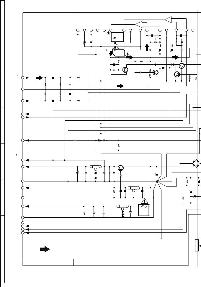
CD-C831W |
|
|
|
|
|
|
|
|
|
|
|
|
|
|
|
|
|
|
|
|
|
|
|
|
|
|
|
|
|
|
|
|
|
|
|
|
|
|
|
|
|
|
|
|
|
|
|
|||
|
|
|
|
|
|
|
|
|
|
|
|
|
IC901 |
|
|
|
|
|
|
|
|
|
|
|
|
|
|
|
|
|
|
|
|
|
|
|
|
+ |
|
|
|
|
|
|
|
|
|
|||
A |
|
|
|
|
|
|
|
|
|
STK407-040B |
|
|
|
|
|
|
|
|
|
|
|
|
|
|
|
|
|
|
|
|
|
|
|
|
|
|
|
|
|
|
|
|||||||||
|
|
|
|
|
|
|
|
|
|
|
|
|
|
|
|
|
|
|
|
|
|
|
|
|
|
|
|
|
|
Ch2 |
|
|
|
|
|
|
|
|
|
|||||||||||
|
|
|
|
|
|
|
|
|
POWER AMP. |
|
(2Ch) |
|
|
|
|
|
|
|
|
|
|
|
|
|
|
|
|
|
|
|
|
|
|
|
|
|
||||||||||||||
|
|
|
|
|
|
|
|
|
|
|
|
|
|
|
|
|
|
+ |
|
|
|
|
|
|
|
|
– |
|
|
|
|
|
|
|
|
|
||||||||||||||
|
|
|
|
|
|
|
|
|
|
–Vcc |
|
–Vcc |
|
+Vcc |
|
|
NC |
|
|
NC |
|
Ch1 |
Out |
|
|
|
Ch2 Out |
Ch1 |
|
|
|
|
|
|
|
|
|
|
|
|
|
|
|
|
|
|
||||
|
|
|
|
|
|
|
|
|
|
|
|
|
|
|
|
|
|
|
|
|
– |
|
|
|
|
|
|
|
|
|
|
|
|
|
|
|
|
|
|
|||||||||||
|
|
|
|
|
|
|
|
|
|
|
|
|
|
|
|
|
|
|
|
|
|
|
|
|
|
|
|
|
|
|
|
|
|
|
|
|
|
|
|
|||||||||||
|
|
|
|
|
|
|
|
|
|
1 |
|
2 |
|
|
3 |
|
|
4 |
|
|
5 |
|
6 |
|
|
|
|
|
7 |
8 |
9 |
10 |
C915 |
11 |
12 |
|
13 C923 14 |
15 |
|
|
||||||||||
|
|
|
|
|
|
|
|
|
|
|
|
|
|
|
|
|
|
|
|
|
|
|
|
R912 |
|
|
|
|
|
|
|
120P |
|
|
|
R921 |
47P |
|
|
|
|
|
||||||||
|
|
|
|
|
|
|
|
|
|
|
|
|
|
|
|
|
|
|
|
|
|
|
|
|
|
|
|
|
|
|
|
|
|
|
|
|
|
|
|
|
|
|
|
|||||||
|
|
|
|
|
|
|
|
|
|
|
|
|
|
|
|
|
|
|
|
|
|
|
|
100(1/4W) |
|
|
|
|
|
C916 |
|
|
|
|
|
|
|
|
|
|
|
|||||||||
|
|
|
|
|
|
|
|
|
|
|
|
|
|
|
|
|
|
|
|
|
|
|
|
|
|
|
|
|
|
|
|
22K |
|
|
|
|
|
|
|
|
||||||||||
|
|
|
|
|
|
|
|
|
|
|
|
|
|
|
|
|
|
|
|
|
|
|
|
|
|
|
|
|
|
|
|
|
|
|
|
|
|
|
|
|
|
|
|
|
||||||
|
|
|
|
|
|
|
|
|
|
C904 |
10/50 |
C907 |
10/50 |
|
|
|
|
|
|
|
|
|
Fusible |
|
|
|
C911 |
|
|
|
15P |
|
|
|
|
|
R923 |
56K |
|
C924 |
15P |
|
|
|
||||||
|
|
|
|
|
|
|
|
|
|
|
|
|
|
|
|
|
|
|
|
|
|
|
|
|
|
|
|
|
R917 |
R918 |
R922 |
680 |
|
|
|
|
||||||||||||||
|
|
|
|
|
|
|
|
|
|
|
|
|
|
|
|
|
|
|
|
|
|
|
|
|
|
100/50 |
|
|
|
|
|
|
|
|||||||||||||||||
|
|
|
|
|
|
|
|
|
|
|
|
|
|
|
|
|
|
|
|
|
|
|
|
|
|
|
|
|
|
|
|
|
|
|||||||||||||||||
|
|
|
|
|
|
|
|
|
|
|
|
|
|
|
|
|
|
|
|
|
|
|
|
|
|
|
|
|
|
56K |
|
680 |
C918 47/50 |
|
|
|
|
|||||||||||||
|
|
|
|
|
|
|
|
|
|
|
|
|
|
|
|
|
|
|
|
|
|
|
|
|
C912 |
|
|
|
R916 |
|
|
|
|
|
||||||||||||||||
|
|
|
|
|
|
|
|
|
|
|
|
|
|
|
|
|
|
|
|
|
|
|
|
|
|
|
|
|
|
|
|
|
|
|
||||||||||||||||
|
|
|
|
|
|
|
|
|
|
|
|
|
|
|
|
|
|
|
|
R913 |
|
|
100/50 |
|
|
|
1K |
|
C917 |
|
|
|
|
|||||||||||||||||
B |
|
|
|
|
|
|
|
|
|
|
|
|
|
|
|
|
|
|
|
|
|
|
|
100 (1/4W) |
|
|
|
|
|
|
|
|
|
|
|
R924 |
1K |
|
|
|
|
|
||||||||
|
|
|
|
|
|
|
|
|
|
|
|
|
|
|
|
|
|
|
|
R925 |
0.1(1W) |
|
|
Fusible |
|
|
R926 |
|
|
|
|
|
47/50 |
|
|
|
|
|
|
|
|
|||||||||
|
|
|
|
|
|
|
|
|
|
|
|
|
|
|
|
|
|
|
|
|
|
|
|
|
R929 |
1K |
|
|
0.1 (1W) |
|
D903 |
|
|
|
D906 |
|
|
|
R939 |
56K |
||||||||||
|
|
|
|
|
|
|
|
|
|
|
|
|
|
|
|
|
|
|
|
|
|
|
|
|
|
|
|
|
|
|
|
|
|
|
|
|
||||||||||||||
|
|
|
|
|
|
|
|
|
|
|
|
|
|
|
|
|
|
|
|
|
|
|
|
|
|
|
|
|
|
|
1SS133 |
|
|
1SS133 |
2SC3331 |
|
||||||||||||||
|
|
|
|
|
|
|
|
|
|
|
|
|
|
|
|
|
|
|
|
|
|
|
|
C921 |
|
|
|
|
C920 |
R930 R928 |
|
|
|
|
|
|
|
|
|
|
|
|
|
|
|
|||||
|
|
|
|
|
|
|
|
|
|
|
|
|
|
|
|
|
|
|
|
|
|
|
|
0.022 |
|
|
|
10K 1K |
|
|
|
|
|
1SS133 |
|
|
|
|
Q906 |
|
|
|
||||||||
|
|
|
|
|
|
|
|
|
|
|
|
|
|
|
|
|
|
|
|
|
|
|
|
R931 |
|
|
|
|
0.022 |
|
|
|
2SC3331 |
D904 |
Q907 |
2SC3331 |
|
|
|
|
|
|||||||||
|
|
|
|
|
|
C901 |
|
|
R905 |
|
|
|
|
|
|
|
|
|
|
|
|
|
|
|
|
|
|
|
|
|
|
|
|
|
|
|||||||||||||||
|
|
|
|
|
|
|
|
|
|
|
|
|
|
|
|
|
|
|
|
10K |
|
|
|
|
|
|
|
|
|
|
|
|
|
|
|
|||||||||||||||
|
|
|
1 |
L |
|
1/50 |
|
|
|
1K |
|
|
|
|
|
|
|
|
|
|
|
|
|
|
|
|
|
|
Q905 |
|
|
|
|
Q904 |
|
|
|
R93 |
||||||||||||
|
|
|
|
|
|
|
|
|
|
|
|
|
|
|
|
|
|
|
|
|
|
|
|
|
|
2SC3331 |
|
|
|
|
|
|
||||||||||||||||||
|
|
|
|
|
|
|
|
|
|
|
|
|
|
|
|
|
|
|
|
|
|
|
|
|
|
|
|
|
|
|
|
|
56 |
|||||||||||||||||
|
|
|
|
R901 |
100K |
|
|
|
|
|
|
|
|
|
|
|
|
|
|
|
|
|
|
|
|
|
|
|
|
|
|
|
|
|
|
|
|
|||||||||||||
|
|
|
|
R902 |
68K |
C902 |
220P |
|
|
|
|
|
|
|
|
|
|
|
|
|
|
|
|
|
|
|
|
|
|
|
|
|
|
|
|
|
|
|
|
|
|
|
|
C938 |
|
|
|
|||
|
|
|
|
|
|
|
|
|
|
|
|
|
|
|
|
|
|
|
|
|
|
|
|
|
|
|
|
|
|
|
|
|
|
|
|
|
|
|
|
47/50 |
|
|
|
|||||||
|
|
|
|
|
|
|
|
|
|
|
|
|
|
|
|
|
|
|
|
|
|
|
|
|
|
|
|
|
|
|
|
|
|
|
|
|
|
|
+B |
|
|
|
|
|
||||||
C |
|
|
2 |
A_GND |
|
|
|
|
|
|
|
|
|
|
|
|
|
|
|
|
|
|
|
|
|
|
|
|
|
|
|
|
|
|
|
|
|
|
|
|
|
|
|
|
|
|
|
|
|
|
|
|
|
|
R904 |
|
|
|
|
|
|
|
|
|
|
|
|
|
|
|
|
|
|
|
|
|
|
|
|
|
|
|
|
|
|
|
|
|
|
|
|
|
|
|
|
|
|
|
|
||
|
|
|
R903 |
100K |
68K |
C905 |
220P |
|
|
|
|
|
|
|
|
|
|
|
|
|
|
|
|
|
|
|
|
|
|
|
|
|
|
|
|
|
|
|
|
|
|
|
|
|
|
|
|
|
||
|
|
|
|
R907 |
|
|
|
|
|
|
|
|
|
|
|
|
|
|
|
|
|
|
|
|
|
|
|
|
|
|
|
|
|
|
|
|
|
|
|
|
|
|
|
|||||||
|
|
|
|
|
|
|
|
|
|
|
|
|
|
|
|
|
|
|
|
|
|
|
|
|
|
|
|
|
|
|
|
|
|
|
|
|
|
|
|
|
|
|
|
|
|
|
|
|
||
|
|
|
3 |
R |
|
|
|
|
|
1K |
|
|
|
|
|
|
|
|
|
|
|
|
|
|
|
|
|
|
|
|
|
|
|
|
|
|
|
|
|
|
|
|
|
|
|
|
|
|
|
|
|
|
|
|
|
C903 |
|
|
|
|
|
|
|
|
|
|
|
|
|
|
|
|
|
|
|
|
|
|
|
|
|
|
|
|
|
|
|
|
|
|
|
|
|
|
|
|
|
|
|
|
|
|
|
|
|
|
|
|
|
|
|
|
|
|
|
|
|
|
|
|
|
|
|
|
|
|
|
|
|
|
|
|
|
|
|
|
|
|
|
|
|
|
|
|
|
|
|
|
|
|
|
|
|
|
|
|
|
|
1/50 |
|
|
|
|
|
|
|
|
|
|
|
|
|
|
|
|
|
|
|
|
|
|
|
|
|
|
|
|
|
|
|
|
|
|
|
|
|
|
|
|
|
|
|
|
|
|
|
|
|
|
+B |
|
|
|
|
|
|
|
|
|
|
|
|
|
|
|
|
|
|
|
|
|
|
|
|
|
|
|
|
|
|
|
|
|
|
|
|
|
|
|
|
|
|
|
|
|
|
|
4 |
SP_DET |
|
|
|
|
|
|
|
|
|
|
|
|
|
|
|
|
|
|
|
|
|
|
|
|
|
|
|
|
|
|
|
|
|
|
|
|
|
|
|
|
|
|
|
|
|
|
|
|
|
SP_RLY |
|
|
|
|
|
|
|
|
|
|
|
|
|
|
|
|
|
|
|
|
|
|
|
|
|
|
|
|
|
|
|
|
|
|
|
|
|
|
|
|
|
|
|
|
|
|
|
|
|
|
5 |
|
|
|
|
|
|
|
|
|
|
|
|
|
|
|
|
|
|
|
|
|
|
|
|
|
|
|
|
|
|
|
|
|
|
|
|
|
|
|
|
|
|
|
|
|
|
|
|
|
|
|
|
|
|
|
|
|
|
|
|
|
|
|
|
|
|
|
|
|
|
|
|
|
|
|
|
|
|
|
|
|
|
|
|
|
|
|
|
|
|
|
|
|
|
|
|
|
|
|
|
|
|
|
|
|
|
+B |
|
|
|
|
|
|
|
|
|
|
|
|
|
|
|
|
|
|
|
|
|
|
|
|
|
|
|
|
|
|
|
|
|
|
|
+B |
|
|
|
|
|
|
D |
|
|
|
|
|
|
|
|
|
|
|
|
|
|
|
|
|
|
|
|
|
|
|
|
|
|
|
|
|
|
|
|
|
|
|
|
|
|
|
|
|
|
|
|
|
|
|
|
|
|
|
|
|
|
|
|
|
|
|
|
|
|
|
|
|
|
–B |
|
|
|
|
|
|
|
|
|
|
|
|
|
|
|
|
|
|
|
|
|
|
|
|
|
|
|
|
|
|
|
|
D |
|
|
|
|
|
|
|
|
|
|
|
|
|
|
|
|
|
|
|
|
|
|
|
|
|
|
|
|
|
|
|
|
|
|
|
|
|
|
|
|
|
|
|
|
|
|
|
|
|
T |
||
|
|
|
|
|
|
|
|
R830 |
|
|
|
C909 |
|
|
|
|
|
|
|
|
|
|
|
|
|
|
|
|
|
|
|
|
|
|
|
|
|
|
|
|
|
|
|
|
|
|
||||
|
|
|
6 |
–15V |
|
|
|
820 (3W) |
|
|
2200/50 |
|
|
|
|
|
|
|
|
|
|
|
|
|
+B1 |
|
|
|
|
|
|
|
|
|
|
|
|
|
|
|
|
|
|
|
||||||
|
|
|
|
|
|
|
|
|
|
|
|
|
|
|
|
|
|
|
|
C910 |
|
|
|
|
|
|
|
|
|
|
|
|
|
|
|
|
|
|
|
|
|
|
|
|
|
|
|
|||
|
P17 12 - G |
SECTION |
|
|
|
|
|
|
|
|
|
|
|
|
|
|
|
|
|
|
|
|
|
R966 |
|
|
|
|
|
|
|
|
|
|
|
|
|
|
|
|
|
|
|
|
|
|||||
|
|
|
|
|
|
|
|
|
|
|
|
|
|
|
|
|
|
|
2200/50 |
|
|
|
|
|
|
|
|
|
|
|
|
|
|
|
|
|
|
|
|
|
|
|
|
|||||||
|
|
|
|
|
|
|
|
|
|
|
|
|
|
|
|
|
|
|
|
|
|
22K |
|
|
|
|
|
|
|
|
|
|
|
|
|
|
|
|
|
|
|
|
|
|||||||
|
|
|
|
|
|
|
|
|
|
|
|
|
|
|
|
|
|
|
|
|
|
|
|
|
|
|
|
|
|
|
|
|
|
|
|
|
|
|
|
|
|
|
|
|
|
|||||
|
|
|
|
|
|
|
|
|
|
|
|
|
|
|
–B |
|
|
|
|
|
|
|
|
|
|
|
|
|
|
|
|
|
|
|
|
|
|
|
|
|
|
|
|
|
|
|
|
|||
|
|
|
|
|
|
|
|
|
|
|
|
|
|
|
|
|
|
|
|
|
|
|
|
|
|
|
|
|
|
|
|
|
|
|
|
|
|
|
|
|
|
|
|
|
|
|
|
|
||
|
2 - D, |
MAIN |
|
M_12V |
|
|
|
|
|
|
|
|
|
|
|
|
|
|
|
|
+B |
|
|
|
VOLTAGE |
|
|
|
|
|
|
|
|
|
|
|
|
|
|
|
|
D803 |
|
D |
||||||
|
7 |
|
|
|
|
|
|
|
|
|
|
|
|
|
|
|
|
|
|
|
REGULATOR |
|
|
|
|
|
|
|
|
|
|
|
|
|
|
|
|
|
||||||||||||
E |
|
|
+B |
|
+B |
|
|
|
|
|
|
|
Q821 |
|
|
|
|
|
|
|
|
Q823 |
|
|
|
|
|
|
|
|
|
|
|
|
|
+B2 |
1N4004S |
|
1 |
|||||||||||
P16 |
TO |
|
|
|
|
|
|
|
|
|
|
|
|
|
|
|
|
|
|
|
|
|
|
|
|
|
|
|
|
|
|
|
|
|
|
|
|
|
|
|||||||||||
|
8 |
+5V |
|
|
|
|
|
|
|
|
|
|
AN78L05 |
|
|
|
|
KTD2058 Y |
|
|
|
|
|
|
|
|
|
|
|
|
|
|
|
|
D804 |
|
D |
|||||||||||||
|
|
|
|
|
|
|
+B |
|
|
|
0.047(ML) |
|
|
3 |
|
|
|
1 |
|
|
|
|
|
|
|
|
|
|
|
|
|
|
|
|
|
|
|
|
|
|
+B |
|
|
|
|
|||||
|
|
|
|
|
|
|
|
47/25 |
|
|
|
|
|
1SS133 |
2 |
|
|
|
|
0.047(ML) |
|
|
|
|
|
|
|
|
|
|
|
|
|
|
|
|
|
|
|
|
|
1N4004S |
|
1 |
||||||
|
|
|
|
|
|
|
|
C830 |
C821 |
|
D820 |
|
|
|
|
|
|
|
|
|
|
|
|
|
|
|
|
|
3300/25 |
|
|
|
|
|
|
|
|
|
||||||||||||
|
|
|
|
D_GND |
|
|
|
|
|
D821 |
1SS133 |
C824 |
R832 |
22K |
C825 |
22/25 |
R825 |
33 |
VOLTAGE |
|
|
|
C829 |
|
|
|
|
|
|
|
|
|
|
|
|
|
|
|||||||||||||
|
|
|
9 |
|
|
|
|
|
REGULATOR |
|
|
|
|
|
|
|
|
R803 |
47K |
|
|
|
|
|
||||||||||||||||||||||||||
|
|
|
|
|
|
|
|
|
|
|
Q824 |
|
|
|
|
|
|
|
|
|
|
|
|
|
|
|||||||||||||||||||||||||
|
|
|
|
A_12V |
|
|
|
|
|
KIA7812P |
|
|
|
|
|
|
|
|
|
|
|
|
MTZJ6.2A |
|
||||||||||||||||||||||||||
|
|
|
|
|
|
|
+B |
|
|
|
|
|
|
|
|
|
|
|
|
|
|
|
|
|
|
|
|
|
|
|
|
|
|
|
|
|
|
|
|
|
|
|
|
|
|
|
||||
|
|
|
10 |
|
|
|
|
|
|
|
|
|
|
|
|
|
|
|
|
|
|
|
|
|
|
|
|
3 |
1 |
|
|
|
|
|
|
|
|
|
|
|
|
|
|
|
100/35 |
ZD801 |
|
|||
|
|
|
|
|
|
|
|
|
|
|
|
|
|
|
|
|
|
|
|
|
|
R827 |
22K |
C826 |
47/25 |
|
|
|
C827 |
|
|
|
|
|
|
|
|
|
|
C802 |
R802 |
|||||||||
|
|
|
|
|
|
|
|
|
|
|
|
|
|
|
|
|
|
|
|
|
|
|
|
|
|
2 |
|
|
|
|
|
|
|
|
|
|
|
|||||||||||||
|
|
|
|
|
|
|
|
|
|
|
|
|
|
|
|
|
|
|
|
|
|
|
|
|
C828 0.1 |
|
0.1 |
|
|
|
|
|
|
|
|
|
|
|||||||||||||
|
|
|
|
|
|
|
|
|
|
|
|
|
|
|
|
|
|
|
|
|
|
|
|
|
(ML) |
|
(ML) |
|
|
|
|
|
|
|
|
|
|
|||||||||||||
|
|
|
|
A_GND |
|
|
|
|
|
|
|
|
|
|
|
|
|
|
|
|
|
|
|
|
|
|
|
|
|
|
|
|
|
|
|
|
|
|||||||||||||
F |
|
|
11 |
|
|
|
|
|
|
|
|
|
|
|
|
|
|
|
|
|
|
|
|
|
|
|
|
|
|
|
|
|
|
|
|
|
|
|
|
|
|
|
|
R801 |
|
|
|
|||
|
|
|
|
|
|
|
|
|
|
|
|
|
|
|
|
|
|
|
|
|
|
|
|
|
|
|
|
|
|
|
|
|
|
|
|
|
|
|
|
|
|
|
12K |
|
|
|
||||
|
|
|
|
|
|
|
|
|
|
|
|
|
|
|
|
|
|
|
|
|
|
|
|
|
|
Q822 |
|
|
|
|
|
|
|
|
|
|
|
|
|
|
|
|
|
|||||||
|
|
|
|
|
|
|
|
|
|
|
|
|
|
|
|
|
|
|
|
|
VOLTAGE |
|
|
|
|
|
|
|
|
|
|
|
|
|
|
|
|
|
|
|
|
|
|
|||||||
|
|
|
|
CD_+B |
|
|
|
|
|
|
|
|
|
|
|
|
|
|
|
|
REGULATOR |
|
KIA7806P |
|
|
|
|
|
|
|
|
|
|
|
|
|
|
|
|
|
|
|
|
|||||||
|
|
|
12 |
|
|
|
|
|
|
|
|
|
|
|
|
|
|
|
|
|
|
|
|
|
|
3 |
|
|
1 |
|
|
|
|
+B |
|
|
|
|
|
|
|
|
|
|
|
|
|
|
R |
|
|
|
|
|
|
|
|
|
|
|
|
|
|
|
|
|
|
|
|
|
|
|
|
|
|
|
2 |
|
|
F832 |
|
|
|
|
|
|
|
|
|
|
|
|
|
|
|
||||||
|
|
|
|
|
|
|
|
|
|
|
|
|
|
|
|
|
|
|
|
0.1(ML) |
|
|
|
D832 |
|
|
C833 |
|
|
|
|
|
|
|
|
|
|
|
|
|
|
|
||||||||
|
|
|
|
|
|
|
|
|
|
|
|
|
|
|
|
|
|
C832 |
|
|
|
|
|
|
|
|
|
|
|
|
|
|
|
|
|
|
|
|
|
|
||||||||||
|
|
|
|
|
|
|
|
|
|
R837 |
10K |
|
C831 |
47/25 |
|
|
|
1SS133 |
|
|
|
0.1 |
T500mA |
|
|
|
|
|
|
|
|
|
|
|
|
|
|
|
|
|||||||||||
|
|
|
|
|
|
|
|
|
|
|
|
|
|
|
D833 |
|
|
|
(ML) |
L 250V |
|
|
|
|
|
|
|
|
|
|
|
|
|
|
|
|
|
|||||||||||||
|
|
|
13 |
CD_GND |
|
|
|
|
|
|
|
|
|
1SS133 |
|
|
|
|
|
|
|
|
|
|
|
|
|
|
|
|
|
|
|
|
|
|
|
|||||||||||||
|
|
|
|
|
|
|
|
|
|
|
|
|
|
|
|
|
|
|
|
|
|
|
|
|
|
|
|
|
|
|
|
|
|
|
|
|
|
|
|
|
|
|
|
|
||||||
|
|
|
|
|
|
|
|
|
|
|
|
|
|
|
|
|
|
|
|
|
|
|
|
|
|
|
|
|
|
|
|
|
|
|
|
|
|
|
|
|
|
|
|
|
|
|
|
|
|
|
|
|
|
14 |
M_GND |
|
|
|
|
|
|
|
|
|
|
|
|
|
|
|
|
|
|
|
|
|
|
|
|
|
|
|
|
|
|
|
|
|
|
|
|
|
|
|
|
|
|
|
|
|
|
|
|
|
–VF |
|
|
|
|
|
|
|
|
|
|
|
|
|
|
|
|
|
|
|
|
|
|
|
|
|
|
|
|
|
|
|
|
|
|
|
|
|
|
|
|
|
|
|
|
|
|
|
|
|
|
15 |
|
|
|
|
|
|
|
|
|
|
|
|
|
|
|
|
|
|
|
|
|
|
|
|
|
|
|
|
|
|
|
|
|
|
|
|
|
|
|
|
|
|
|
|
|
|
|
|
|
|
VF2 |
|
|
|
|
|
|
|
|
|
|
|
|
|
|
|
|
|
|
|
|
|
|
|
|
|
|
|
|
|
|
|
|
|
|
|
|
|
|
|
|
|
|
|
|
|
|
|
|
|
|
16 |
|
|
|
|
|
|
|
|
|
|
|
|
|
|
|
|
|
|
|
|
|
|
|
|
|
|
|
|
|
|
|
|
|
|
|
|
|
|
|
|
|
|
|
|
|
|
|
|
|
|
VF1 |
|
|
|
|
|
|
|
|
|
|
|
|
|
|
|
|
|
|
|
|
|
|
|
|
|
|
|
|
|
|
|
|
|
|
|
|
|
|
|
|
|
|
|
|
|
|
|
G |
|
|
17 |
|
|
|
|
|
|
|
|
|
|
|
|
|
|
|
|
|
|
|
|
|
|
|
|
|
|
|
|
|
|
|
|
|
|
|
|
|
|
|
|
|
|
|
|
|
|
|
|
|
|
|
|
|
|
|
|
|
|
|
|
|
|
|
|
|
|
|
|
|
|
|
|
|
|
|
|
|
|
|
|
|
|
|
|
|
|
|
|
|
|
|
|
|
|
|
|
||
|
|
|
|
|
|
|
|
|
|
|
|
|
|
|
|
|
|
|
|
|
|
|
|
|
|
|
|
|
|
|
|
|
|
|
|
|
|
|
|
|
|
|
|
|
|
|
DISPLAY PWB |
|
|
|
|
|
|
|
|
|
FM SIGNAL |
|
|
|
|
|
|
|
|
|
|
|
|
|
|
|
|
|
|
|
|
|
|
|
|
|
|
|
|
|
|
|
|
|
|
|
|
|
|
P21 12 - E |
CNS806 |
|
|||
|
|
|
|
|
|
|
|
|
|
|
|
|
|
|
|
|
|
|
|
|
|
|
|
|
|
|
|
|
|
|
|
|
|
|
|
|
|
|
|
|
|
|
|
|
|
|
|
|||
|
|
|
|
|
|
|
|
|
|
|
|
|
|
|
|
|
|
|
|
|
|
|
|
|
|
|
|
|
|
|
|
|
|
|
|
|
|
|
|
|
|
|
|
|
|
|
|
TO |
|
|
MAIN PWB-A1(2/2)
H
• NOTES ON SCHEMATIC DIAGRAM can be found on page 12.
|
1 |
2 |
3 |
4 |
5 |
6 |
Figure 18 SCHEMATIC DIAGRAM (3/9)
– 18 –
 Loading...