


CD-C1W,CP-C1W
SERVICE MANUAL
No. YS792CDC1W///
CD-C1W
CP-C1W
●SRS technology Licensed from SRS Labs. SRS technology holds the following patents: U.S. Patent No. 4,748,669 and U.S. Patent No. 4,841,572.
●

 , the SRS Logo (●) and the SOUND RETRIEVAL SYSTEM
are registered trademarks of SRS Labs, Inc. in the United States.
●Dolby noise reduction manufactured under license from Dolby Laboratories Licensing Corporation.
● "DOLBY" and the double-D symbol |
|
are trademarks |
of Dolby Laboratories Licensing Corporation.
•In the interests of user-safety the set should be restored to its original condition and only parts identical to those specified should be used.
CONTENTS |
|
|
Page |
SAFETY PRECAUTION FOR SERVICE MANUAL ................................................................................................................ |
2 |
VOLTAGE SELECTION .......................................................................................................................................................... |
2 |
AC POWER SUPPLY CORD AND AC PLUG ADAPTOR ...................................................................................................... |
2 |
SPECIFICATIONS ................................................................................................................................................................. |
3 |
NAMES OF PARTS ............................................................................................................................................................... |
4 |
OPERATION MANUAL .......................................................................................................................................................... |
6 |
DISASSEMBLY ...................................................................................................................................................................... |
8 |
REMOVING AND REINSTALLING THE MAIN PARTS ....................................................................................................... |
11 |
ADJUSTMENT ..................................................................................................................................................................... |
12 |
TEST MODE ......................................................................................................................................................................... |
14 |
NOTES ON SCHEMATIC DIAGRAM .................................................................................................................................. |
16 |
TYPES OF TRANSISTOR AND LED .................................................................................................................................... |
16 |
BLOCK DIAGRAM ............................................................................................................................................................... |
17 |
SCHEMATIC DIAGRAM/WIRING SIDE OF P.W.BOARD ................................................................................................... |
20 |
WAVEFORMS OF CD CIRCUIT .......................................................................................................................................... |
42 |
TROUBLE SHOOTING ........................................................................................................................................................ |
43 |
FUNCTION TABLE OF IC .................................................................................................................................................... |
46 |
FL SEGMENT ...................................................................................................................................................................... |
55 |
PARTS GUIDE/EXPLODED VIEW |
|
SHARP CORPORATION |
This document has been published to be used |
for after sales service only. |
|
– 1 – |
The contents are subject to change without notice. |
|
CD-C1W,CP-C1W
SAFETY PRECAUTION FOR SERVICE MANUAL
WARNINGS
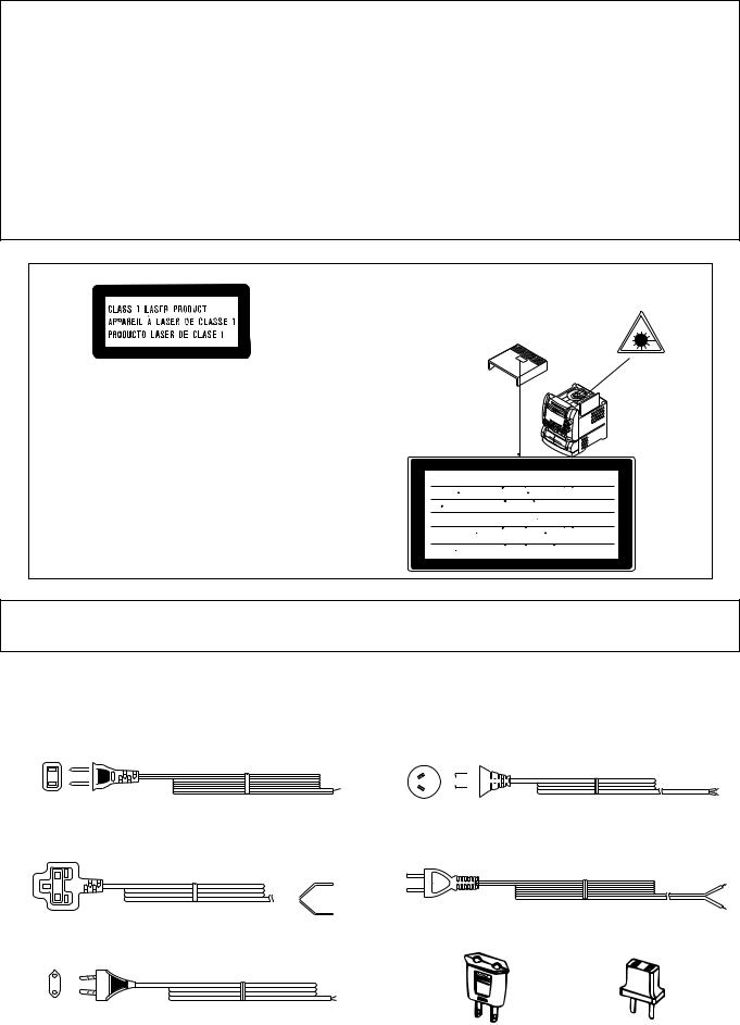
THE AEL (ACCESSIBLE EMISSION LEVEL) OF THE LASER POWER OUTPUT IS LESS THAN CLASS 1 BUT THE LASER COMPONENT IS CAPABLE OF EMITTING RADIATION EXCEEDING THE LIMIT FOR CLASS 1. THEREFORE IT IS IMPORTANT THAT THE FOLLOWING PRECAUTIONS ARE OBSERVED DURING SERVICING TO PROTECT YOUR EYES AGAINST EXPOSURE TO THE LASER BEAM.
1-WHEN THE CABINET IS REMOVED, THE POWER IS TURNED ON WITDOUT A COMPACT DISC IN POSITION AND THE PICK-UP IS ON THE OUTER EDGE THE LASER WILL LIGHT FOR SEVERAL SECONDS TO DETECT A DISC. DO NOT LOOK INTO THE PICK-UP LENS.
2-THE LASER POWER OUTPUT OF THE PICK-UP UNIT AND REPLACEMENT SERVICE PARTS ARE ALL FACTORY PRE-SET BEFORE SHIPMENT.
DO NOT ATTEMPT TO RE-ADJUST THE LASER PICK-UP UNIT DURING REPLACEMENT OR SERVICING. 3-UNDER NO CIRCUMSTANCES STARE INTO THE PICK-UP LENS AT ANY TIME.
4-CAUTION-USE OF CONTROLS OR ADJUSTMENTS, OR PERFORMANCE OF PROCEDURES OTHER THAN THOSE SPECIFIED HEREIN MAY RESULT IN HAZARDOUS RADIATION EXPOSURE.
CAUTION |
Laser Diode Properties |
|
Material: GaAIAs |
|
Wavelength: 780 nm |
|
Emission Duration: continuous |
|
Laser Output: max. 0.6 mW |
●This Mini Component System is classified as a CLASS 1 LASER product.
●The CLASS 1 LASER PRODUCT label is located on the rear cover.
●Use of controls or adjustments or performance of procedures other than those specified herein may result in hazardous radiation exposure.
As the laser beam used in this compact disc player is harmful to the eyes, do not attempt to disassemble the cabinet. Refer servicing to qualified personnel only.
CAUTION-INVISIBLE LASER RADIATION WHEN OPEN. DO NOT STARE INTO BEAM OR VIEW DIRECTLY WITH OPTICAL INSTRUMENTS.
VARNING-OSYNLIG LASERSTRALNING NAR DENNA DEL AR OPPNAD. STIRRA EJ IN I STRALEN OCH BETRAKTA EJ STRALEN MED OPTISKA INSTRUMENT.
ADVERSEL-USYNLIG LASERSTRALING VED ABNING. SE IKKE IND I STRALEN-HELLER IKKE MED OPTISKE INSTRUMENTER.
VARO! AVATTAESSA OLET ALTTIINA NAKYMATON LASERSATEILYLLE. ALA TUIJOTA SATEESEEN ALAKA KATSO SITA OPTISEN LAITTEEN LAPI.
VARNING-OSYNLIG LASERSTRALNING NAR DENNA DEL AR OPPNAD. STIRRA EJ IN I STRALEN OCH BETRAKTA EJ STRALEN GENOM OPTISKT INSTRUMENT.
ADVERSEL-USYNLIG LASERSTRALING NAR DEKSEL APNES. STIRR IKKE INN I STRALEN ELLER SE DIREKTE MED OPTISKE INSTRUMENTER.
VARO ! Avattaessa ja suojalukitus ohitettaessa olet alttiina näkymättömälle lasersäteilylle. Älä katso säteeseen. VARNING! Osynlig laserstralning när denna del är öppnad och spärren är urkopplad. Betrakta ej strälen.
VOLTAGE SELECTION
The voltage selector is located on the AC voltage selector box. If adjustment is necessary, use a screwdriver in order to turn the selector in either direction until the correct voltage figure is displayed in the window next to the adjustment screw.
QACCA0001AW00 |
|
|
|
|
||||||||
|
92LCoRDA1387C |
|||||||||||
|
|
|
|
|
|
|
|
|
|
|
|
|
|
|
|
|
|
|
|
|
|
|
|
|
|
|
|
|
|
|
|
|
|
|
|
|
|
|
|
|
|
|
|
|
|
|
|
|
|
|
|
QACCB0005AW00 |
|
|
|
|
||||||||
|
92LCoRDT1699A |
|||||||||||
|
|
|
|
|
|
|
|
|
|
|
|
|
|
|
|
|
|
|
|
|
|
|
|
|
|
|
|
|
|
|
|
|
|
|
|
|
|
|
|
|
|
|
|
|
|
|
|
|
|
|
|
QACCE0008AW00 |
92LPLUG155A |
92LPLUG027 |
Figure 2 AC POWER SUPPLY CORD AND AC PLUG ADAPTOR
– 2 –

CD-C1W,CP-C1W
SPECIFICATIONS
CD-C1W
● General
Power source: |
AC 110/127/220/230-240 V, |
Power |
50/60 Hz |
|
|
consumption: |
500 W |
Dimensions: |
Width; 270 mm (10-5/8") |
|
Height; 356 mm (14-3/16") |
Weight: |
Depth; 355 mm (14") |
10.5 kg (23.1 lbs.) |
● Amplifier section
Output power: |
PMPO; 2400 W (total) |
|
MPO; 440 W (220 W + 220 |
|
W) |
|
(10 % T.H.D.) |
|
RMS; 300 W (150 W + 150 |
|
W) |
Input terminals: |
(10 % T.H.D.) |
Video/Auxiliary (audio sig- |
|
Output terminals: |
nal); 500 mV/47 kohms |
Speakers; 6 ohms |
|
|
Headphones; 16-50 ohms |
|
(recommended; 32 ohms) |
|
Line output; 500 mV/47 |
|
kohms |
● Compact disc player section
Type: |
3-disc multi-play compact |
Signal readout: |
disc player |
Non-contact, 3-beam semi- |
|
Rotational speed: |
conductor laser pickup |
200 - 500 rpm CLV, Approx. |
|
Error correction: |
CIRC (Cross Interleave |
Quantization: |
Reed-Solomon Code) |
16-bit linear |
|
Filter: |
4-times oversampling digital |
D/A converter: |
filter |
1-bit D/A converter |
|
Frequency |
|
response: |
20 - 20,000 Hz |
Dynamic range: |
90 dB (1 kHz) |
Wow and flutter: |
Unmeasurable |
|
(less than 0.001% W. peak) |
● Tuner section
Frequency range: |
FM; 88 - 108 MHz |
|
|
SW2; 9.5 |
- 21.85 MHz |
|
SW1; 3.2 |
- 7.3 MHz |
|
MW; 531 - 1,602 kHz |
|
● Cassette deck section
Type: |
Compact cassette tape |
Frequency response: |
50 - 14,000 Hz (Normal tape) |
|
50 - 15,000 Hz (CrO2 tape) |
Motor: |
DC motor with electronic governor × 1 |
Signal/noise ratio: |
55 dB (TAPE 1, playback, Dolby NR |
|
off) |
|
50 dB (TAPE 2, recording/playback, |
|
Dolby NR off) |
|
Dolby NR effect; 10 dB |
Bias and erasure |
(at over 5 kHz) |
|
|
system: |
AC |
Tape speed: |
4.76 cm/sec. (1-7/8 ips.) |
Wow and flutter: |
0.15 % (WRMS) |
Heads: |
TAPE-1: Playback × 1 |
|
TAPE-2: Record/playback × 1 |
|
Erase × 1 |
|
|
CP-C1W |
|
● Speaker section |
|
Type: |
3-way type [20 cm (7-7/8") woofer, |
|
8 cm (3-3/16") tweeter and super |
Rated input power: |
tweeter] |
150 W |
|
Maximum input power: 300 W |
|
Impedance: |
6 ohms |
Dimensions: |
Width; 295 mm (11-5/8") |
|
Height; 361 mm (14-1/4") |
Weight: |
Depth; 378 mm (14-15/16") |
6.7 kg (14.8 lbs.)/each |
|
– 3 –
CD-C1W,CP-C1W
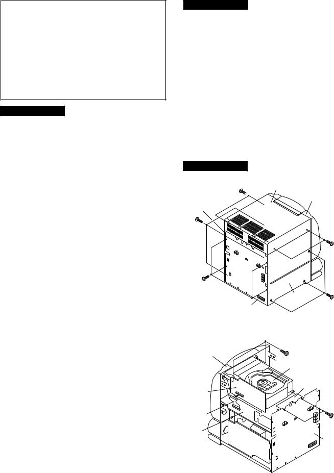
NAMES OF PARTS
CD-C1W
■Front panel
1.Disc 1 Select/Direct Play Button
2.Disc 1 Open/Close Button
3.Disc 2 Select/Direct Play Button
4.Disc 2 Open/Close Button
5.Disc 3 Select/Direct Play Button
6.Disc 3 Open/Close Button
7.Disc Trays
8.Function Selector Buttons
9.Remote Control Sensor
10.On/Stand-by Button
11.Volume Control
12.Extra Bass Button
13.3D Surround Mode Button
14.3D Surround Pass Button
15.Equalizer Selector/Demo Mode Button
16.(CD) Random Play Indicator
17.(CD/TUNER) Memory Indicator
18.(TAPE 2) Direction Indicators
19.(CD) Pause Indicator
20.(CD) Disc Number Indicators
21.(CD) Music Schedule Indicators
22.SRS Indicator
23.Extra Bass Indicator
24.Timer Play Indicator
25.Timer Record Indicator
26.Sleep Indicator
27.(TAPE) Dolby NR Indicator
28.(TAPE) Reverse Mode Indicator
29.(TAPE) Record Indicator
30.(CD) Play Indicator
31.(CD) Repeat Indicator
32.Spectrum Analyzer/Volume Level Indicator
33.FM Stereo Indicator
34.FM Stereo Mode Indicator
1 |
2 |
3 |
4 |
5 |
6 |
7 |
8 |
|
|
|
|
|
11 |
9 |
|
|
|
|
|
12 |
|
|
|
|
|
13 |
|
10 |
|
|
|
|
|
14 |
|
|
|
|
|
15 |
|
|
|
|
|
|
|
18 |
24 |
16 17 19 20 |
21 22 23 25 2627 |
28 2930 31 |
32 |
33 34 |
35.(CD) Clear Button
36.Memory/Set Button
37.(TAPE) Reverse Mode Button
38.(TAPE) Reverse Play Button
39.(TUNER) Tuning Down Button (CD) Track Down/Review Button (TAPE) Fast Wind Button
40.Jog Dial
41.(TUNER) Tuning Up Button (CD) Track Up/Cue Button (TAPE) Fast Wind Button
42.(CD) Play/Repeat Button (TAPE) Forward Play Button
43.(TAPE) Record Pause Button
44.(TAPE) Editing Speed Selector Buttons
45.Headphone Socket
46.Clock Button
47.Timer Button
48.Sleep Button
49.(CD) Pause Button
50.(CD/TAPE) Stop Button
51.(TAPE) Dolby NR Button
52.(TAPE 1) Cassette Compartment
53.(TAPE 2) Cassette Compartment
35 36 37 38 39 40 41 42 43 44
4546 47 48 49 50 51
52 53
– 4 –
■Rear panel
1.Video/Auxiliary (Audio Signal) Input Sockets
2.Line Output Sockets
3.Span Selector Switch
4.AC Power Lead
5.AC Voltage Selector
6.FM 75 Ohms Aerial Terminal
7.Aerial Earth Terminal
8.SW1/SW2/MW Aerial Terminal
9.Speaker Terminals
■Remote control
1.Remote Control Transmitter LED
●CD control section
2.Track Down/Review Button
3.Track Up/Cue Button
4.CD Select/Direct Play Buttons
5.Play/Repeat Button
6.Stop Button
7.Memory Button
8.Clear Button
9.Random Button
10.Pause Button
●Tuner control section
11.Preset Up/Down Buttons
●Tape control section
12.Reverse Play Button
13.Record Pause Button
14.Stop Button
15.Forward Play Button
16.Fast Wind Buttons
●Common section
17.3D Surround Pass Button
18.3D Surround Mode Button
19.Function Selector Buttons
20.Balance Buttons
21.On/Stand-by Button
22.Dimmer Button
23.Equalizer Mode Button
24.Extra Bass Button
25.Volume Up/Down Button
CP-C1W
■Speaker section
10.Tweeter
11.Woofer
12.Super Tweeter
13.Bass Reflex Duct
14.Speaker Terminals
CD-C1W,CP-C1W
1 |
|
|
2 |
|
|
|
3 |
||||||||||||||||
|
|
|
|
|
|
|
|
|
|
|
|
|
|
|
|
|
|
|
|
|
|
|
|
|
|
|
|
|
|
|
|
|
|
|
|
|
|
|
|
|
|
|
|
|
|
|
|
|
|
|
|
|
|
|
|
|
|
|
|
|
|
|
|
|
|
|
|
|
|
|
|
|
|
|
|
|
|
|
|
|
|
|
|
|
|
|
|
|
|
|
|
|
|
|
|
|
|
|
|
|
|
|
|
|
|
|
|
|
|
|
|
|
|
|
|
|
|
|
|
|
|
|
|
|
|
|
|
|
|
|
|
|
|
|
|
|
|
|
|
|
|
|
|
|
6 |
4 |
7 |


 8 5
8 5 


 9
9
1
|
4 |
|
2 |
5 |
|
3 |
6 |
|
7 8 |
9 10 |
|
12 |
11 |
|
14 |
||
13 |
15 |
|
|
16 |
|
|
17 18 |
|
|
23 |
|
19 |
24 |
|
|
||
20 |
|
|
21 |
25 |
|
22 |
||
|
10 


 12
12
|
14 |
11 |
13 |
– 5 –
CD-C1W,CP-C1W
OPERATION MANUAL
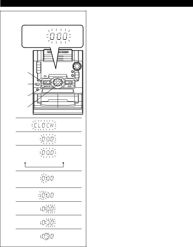
SETTING THE CLOCK
In this example, the clock is set for the 24-hour (0:00) system.
MEMORY/
SET
ON/STAND-
BY
CLOCK
Jog dial
2
3
4
0:00 
 AM 0:00
 AM 12:00
5
6
7
8
9
1 Press the ON/STAND-BY button to enter the stand-by mode.
2 Press the CLOCK button.
3 Within 5 seconds, press the MEMORY/SET button.
4 Turn the jog dial to select the time display mode. "0:00" → The 24-hour display will appear.
(0:00 - 23:59)
"AM 12:00" → The 12-hour display will appear. (AM or PM 12:00 - 11:59)
"AM 0:00" → The 12-hour display will appear. (AM or PM 0:00 - 11:59)
●Note that this can only be set when the unit is first installed or it has been reset (see page 25).
5 Press the MEMORY/SET button.
6 Adjust the hour by turning the jog dial.
●Turn the dial one click to advance the time by 1 hour. Keep turning the dial to advance continuously.
●When the 12-hour display is selected, "AM" will change automatically to "PM".
7 Press the MEMORY/SET button.
8 Adjust the minutes by turning the jog dial.
●Turn the dial one click to advance the time by 1 minute. Keep turning the dial to advance continuously.
●The hour setting will not advance even if minutes advance from "59" to "00".
9 Press the MEMORY/SET button.
●The clock starts operating from "0" seconds. (Seconds are not displayed.)
Note:
●In the event of a power failure or when the AC power lead is disconnected, the clock display will go out.
When the AC power supply is restored, the clock display will flash on and off to indicate the time when the power failure occurred or when the AC power lead was disconnected.
If this happens, follow the procedure below to change the clock time.
To change the clock time:
When the unit is in the stand-by mode:
Press the MEMORY/SET button.
Perform steps 6 - 9 above. When the unit is on:
Press the CLOCK button.
Within 5 seconds, press the MEMORY/SET button.
Perform steps 6 - 9 above.
To see the time display:
Press the CLOCK button.
● The time display will appear for about 5 seconds.
To change the time display mode:
Perform steps 1 - 2 in the section "RESETTING THE MICROCOMPUTER", on page 25.
Perform steps 1 - 9 above.
– 6 –
(Continued)
SPAN
SELECTOR
FM/MW
(kHz)
100/10
50/9
– 7 –
(Continued)
0.2 m - 6 m (8" - 20')
15
15
■ FM/MW interval (span)
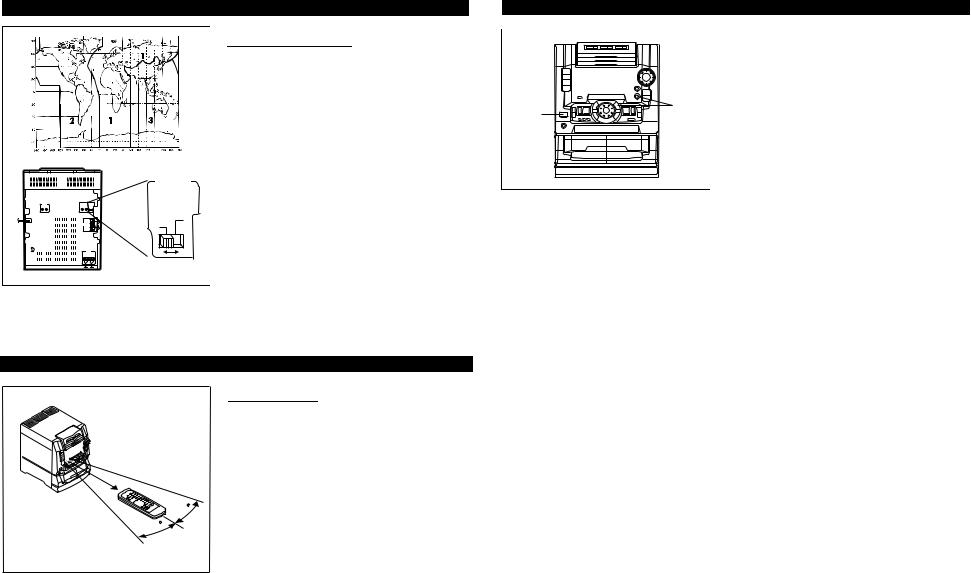
The International Telecommunication Union (ITU) has established that member countries should maintain either a 10 kHz or a 9 kHz interval between broadcasting frequencies of any MW station. The illustration shows the 9 kHz interval zones (regions 1 and 3), and the 10 kHz interval zone (region 2).
Before using the unit, set the SPAN SELECTOR switch (on the rear panel) to MW tuning interval (span) of your area.
To change the tuning zone:
1 Press the ON/STAND-BY button to enter the stand-by mode.
2 Set the SPAN SELECTOR switch to "50/9" for 9 kHz MW interval (50 kHz FM interval), and "100/10" for 10 kHz MW interval (100 kHz FM interval).
3 Press and hold down the button, the EQ/DEMO button and the ON/STAND-BY button all at the same time. Hold them for at least 1 second.
Caution:
●The operation explained above will erase all data stored in memory including clock and timer settings, and tuner and CD presets.
■ Remote control
Notes concerning use:
●Replace the batteries if control distance decreases or operation becomes erratic.
●Periodically clean the transmitter LED on the remote control and the sensor on the main unit with a soft cloth.
●Exposing the sensor on the main unit to strong light may interfere with operation. Change the lighting or the direction of the unit.
●Keep the remote control away from moisture, excessive heat, shock, and vibrations.
RESETTING THE MICROCOMPUTER
1,2 |
2 |
|
Reset the microcomputer under the following conditions:
●To erase all of the stored memory contents (clock and timer settings, and tuner and CD presets).
●If the display is not correct.
●If the operation is not correct.
1 Press the ON/STAND-BY button to enter the stand-by mode.
2 Press and hold down the button, the EQ/DEMO button and the ON/STAND-BY button all at the same time. Hold them for at least 1 second.
C1W-C1W,CP-CD
CD-C1W,CP-C1W
DISASSEMBLY
Caution on Disassembly
Follow the below-mentioned notes when disassembling the unit and reassembling it, to keep it safe and ensure excellent performance:
1.Take cassette tape and compact disc out of the unit.
2.Be sure to remove the power supply plug from the wall outlet before starting to disassemble the unit.
3.Take off nylon bands or wire holders where they need be removed when disassembling the unit. After servicing the unit, be sure to rearrange the leads where they were before disassembling.
4.Take suff cient care on static electricity of integrated circuits and other circuits when servicing.
CD-C1W
STEP |
REMOVAL |
|
PROCEDURE |
FIGURE |
|||||
1 |
Top Cabinet |
1. |
Screw ....................... |
(A1) x4 |
8-1 |
||||
|
|
|
|
|
|
|
|
|
|
2 |
Side Panel |
1. |
Screw ....................... |
(B1) x6 |
8-1 |
||||
|
(Left/Right) |
2. |
Screw ...................... |
(B2) x4 |
|
||||
|
|
|
|
|
|
|
|
|
|
3 |
CD Changer Block |
1. |
Flat cable ................. |
(C1) x1 |
8-2 |
||||
|
|
2. |
Screw ....................... |
(C2) x2 |
|
||||
|
|
3. |
Screw ....................... |
(C3) x2 |
|
||||
4 |
Tuner PWB |
1. |
Screw ....................... |
(D1) x8 |
9-1 |
||||
|
|
2. |
Screw ....................... |
(D2) x1 |
|
||||
|
|
3. |
Screw ....................... |
(D3) x4 |
|
||||
|
|
|
|
|
|
|
|
|
|
5 |
Main PWB |
1. |
Socket ...................... |
(E1) x3 |
9-1 |
||||
|
|
2. |
Flat Cable ................ |
(E2) x1 |
|
||||
|
|
3. |
Flat Wire ................... |
(E3) x2 |
|
||||
|
|
4. |
Screw ....................... |
(E4) x2 |
|
||||
|
|
5. |
Screw ....................... |
(E5) x2 |
|
||||
|
|
|
|
|
|
|
|
|
|
6 |
Front Panel |
1. |
Flat Wire ................... |
(F1) x2 |
9-1 |
||||
|
|
2. |
Screw ....................... |
(F2) x1 |
|
||||
|
|
3. |
Screw ....................... |
(F3) x2 |
|
||||
|
|
|
|
|
|
|
|
|
|
7 |
Display PWB |
1. |
Knob ......................... |
(G1) x2 |
9-2 |
||||
|
|
2. |
Nut ........................... |
(G2) x1 |
|
||||
|
|
3. |
Screw ................... |
(G3) x12 |
|
||||
|
|
|
|
|
|
|
|
|
|
8 |
CD Switch PWB |
1. |
Screw ...................... |
(H1) x3 |
9-2 |
||||
|
|
|
|
|
|
|
|
|
|
9 |
Headphones PWB |
1. |
Screw ....................... |
(J1) x1 |
9-2 |
||||
|
|
|
|
|
|
|
|
|
|
10 |
Tape Mechanism |
1. |
Open the cassette holder |
|
|
|
9-2 |
||
.... |
|||||||||
|
|
2. |
Screw ....................... |
(K1) x6 |
|
||||
|
|
|
|
|
|
|
|
|
|
11 |
Power Amp. PWB |
1. |
Socket ...................... |
(L1) x1 |
9-3 |
||||
|
|
2. |
Screw ....................... |
(L2) x4 |
|
||||
|
|
3. |
Screw ....................... |
(L3) x2 |
|
||||
12 |
Power Supply |
1. |
Screw ..................... |
(M1) x1 |
9-4 |
||||
|
PWB |
2. |
Screw ..................... |
(M2) x4 |
|
||||
|
|
|
|
|
|
|
|
|
|
13 |
CD Changer Holder |
1. |
Screw ....................... |
(N1) x3 |
9-4 |
||||
|
|
|
|
|
|
|
|
|
|
14 |
CD Servo PWB |
1. |
Socket ...................... |
(P1) x6 |
9-5 |
||||
|
(Note) |
2. |
Screw ....................... |
(P2) x3 |
|
||||
|
|
|
|
|
|
|
|
|
|
15 |
Tray Switch PWB |
1. |
Screw ...................... |
(Q1) x1 |
9-5 |
||||
|
|
|
|
|
|
|
|
|
|
16 |
CD Mechanism |
1. |
Screw ....................... |
(R1) x2 |
10-1 |
||||
|
|
2. |
Top Bord .................. |
(R2) x1 |
|
||||
|
|
3. |
Disc Holder .............. |
(R3) x1 |
|
||||
|
|
4. |
Disc Tray .................. |
(R4) x3 |
|
||||
|
|
5. |
Screw ....................... |
(R5) x1 |
|
||||
|
|
6. |
Mechanism Holder |
|
|
|
|
|
|
|
|
|
|
|
|
|
|||
|
|
|
.......................Guide |
(R6) x1 |
|
||||
|
|
7. |
Screw ....................... |
(R7) x2 |
|
||||
|
|
8. |
Mechanism Holder |
|
|
|
|
|
|
|
|
............... |
|
|
|
|
|
||
|
|
|
Bracket |
|
|
|
|
||
|
|
|
|
(R8) x1 |
|
||||
|
|
9. |
Mechanism Holder ... |
(R9) x1 |
|
||||
|
|
10. Screw ................... |
(R10) x4 |
|
|||||
|
|
|
|
|
|
|
|
|
|
Note : After removing the connector for the optical pickup fromthe connector wrap the conductive aluminium foil around the front end of connector so as to protect the optical pickup from electrostatic damage.
CP-C1W
STEP |
REMOVAL |
|
|
PROCEDURE |
|
FIGURE |
|
|
|
|
|
|
|
1 |
Front Panel |
1. Net ........................... |
(A1) x1 |
10-2 |
||
|
|
2. |
Net Holder ............... |
(A2) x4 |
|
|
|
|
3. |
Screw ...................... |
(A3) x4 |
|
|
|
|
4. |
Screw ...................... |
(A4) x2 |
|
|
|
|
|
|
|
|
|
2 |
Speaker |
1. Screw ...................... |
(B1) x2 |
10-3 |
||
|
|
2. |
Screw ...................... |
(B2) x2 |
|
|
|
|
3. |
Bracket .................... |
(B3) x1 |
|
|
|
|
4. |
Screw ...................... |
(B4) x2 |
|
|
|
|
5. |
Screw ...................... |
(B5) x4 |
|
|
|
|
|
|
|
|
|
CD-C1W
Top Cabinet
(A1)x2
Ø3x12mm 

Front Panel
Side Panel (Right)
(B1)x3 |
|
Ø3x10mm |
(A1)x2 |
|
Ø3x12mm |
(B2)x4 |
|
|
Ø3x10mm |
|
|
|
Side Panel |
|
|
(Left) |
(B1)x3 |
|
Rear Panel |
Ø3x10mm |
|
Figure 8-1 |
|
Front Panel |
(C3)x2 |
|
Ø3x12mm |
|
|
|
|
|
|
CD Changer Block |
|
|
CD Changer |
|
CD Servo |
Holder |
|
|
|
|
PWB |
|
|
(C1)x1 |
|
|
|
|
(C2)x2 |
Main |
|
Ø3x10mm |
|
|
|
PWB |
|
Rear |
|
|
|
|
|
Panel |
Figure 8-2
– 8 –
|
(E5)x1 |
|
(E4)x1 |
Ø3x8mm |
|
|
|
|
Ø3x10mm |
(E3)x2 |
|
(F1)x1 |
|
Display PWB |
Power |
|
Front Panel |
CD Changer Block |
PWB |
|
|
|
|
|
|
|
|
(E1)x1 |
Main PWB |
|
|
Pull |
|
|
|
|
|
|
(D2)x1 |
(E1)x2 |
(E4)x1 |
|
Ø3x10mm |
(E2)x1 |
Ø3x10mm |
|
Rear
Panel 


 (E5)x1
Ø3x8mm
 Tuner
Tuner 
 PWB
PWB
 (F1)x1
|
|
|
Lug Wire |
(N1)x1 |
|
|
|
(F2)x1 |
|
|
|
|
Ø3x6mm |
ø3x10mm |
(D1)x8 |
Power |
(D3)x4 |
(F3)x2 |
|
Ø3x10mm |
|
|||
Ø3x10mm |
|
|||
Ø3x10mm |
AMP. PWB |
|
||
|
|
|
Figure 9-1
CD Switch PWB
(G1)x2
Front Panel
|
Washer |
|
|
|
(G2)x1 |
CD Changer |
|
(H1)x3 |
Block |
||
|
|||
Ø3x10mm |
|
|
|
(G3)x12 |
Display |
|
|
PWB |
|
||
Ø3x10mm |
Headphones |
|
|
|
PWB |
Tray |
|
|
|
||
|
Open |
Switch |
|
|
PWB |
||
|
|
Tape Mechanism |
(J1)x1 |
(Q1)x1 |
ø2x7mm |
||
(K1)x6 |
Ø3x8mm |
|
Cassette |
|
|
Ø3x10mm |
|
|
Holder (Left/Right) |
|
|
Lug Wire |
|
CD-C1W,CP-C1W
(N1)x2
ø3x10mm
CD Servo PWB
CD Changer Holder
Figure 9-4
CD Servo PWB
(P1)x3
(P2)x3
ø3 x10mm
(P1)x3
Figure 9-5
Figure 9-2
(M1)x1
Ø3x10mm
(M2)x4 |
(L3)x1 |
|
|
Ø3x6mm |
|
||
Ø4x8mm |
|
||
|
|
||
Power Supply |
(L1)x1 |
(L2)x4 |
|
PWB |
|||
|
|||
|
Ø3x10mm |
||
|
|
(L3)x1
Ø3x6mm
Power AMP. PWB
Figure 9-3
– 9 –
CD-C1W,CP-C1W
|
(R7) x2 |
|
ø2 x6mm |
Push the pawl of disc tray |
|
with a proper screwdriver. |
(R8) x1 |
Back surface
Pawl
Pawl

 Disc Tray 1 Disc Tray 3
Disc Tray 2
(After drawing out the disc trays 1, 2, and 3, turn over the mechanism unit, push two pawls, and remove successively the three disc trays from the mechanism unit, starting with the disc tray 3. Thereby the CD mechanism shown in the right figure can be removed.)
CP-C1W
(R3) x1
 (R1) x2
ø2 x7mm (R5) x1 ø2.6 x12mm
Spring
(R2) x1
Normal state
Disc Tray 1
(R4) x3 |
Disc Tray 2 |
|
Disc Tray 3 |
||
|
Figure 10-1
Push.
Pawl
(R6) x1
(R9) x1
CD
Mechanism
(R10) x4 ø2.6 x10mm
Turn clockwise the main cam to raise the CD mechanism up to the uppermost position.
1 |
Press in turns the arrow |
|
parts, starting with the |
||
2 |
||
uppermost one, to |
||
3 |
||
withdraw the disc trays |
||
|
|
Driver |
(B3)x1 |
|
|
|
||
(A4)x2 |
Tweeter |
(B2)x2 |
|
Super |
ø3x10mm |
||
ø4x20mm |
|||
|
Tweeter |
(B4)x2 |
|
|
|
ø3x10mm |
(A3)x4
ø4x25mm
(A2)x4
|
(B1)x2 |
Front |
|
|
Speaker |
Panel |
|
|
|
ø3x10mm |
|
|
||
|
|
|
||
Box |
(B5)x4 |
|
|
|
|
|
Speaker |
||
Front Panel |
|
ø4x12mm |
Woofer |
|
|
|
Box |
||
|
|
|
||
|
|
|
|
|
(A1)x1 |
|
|
|
|
Figure 10-2 |
|
|
Figure 10-3 |
|
– 10 –
CD-C1W,CP-C1W
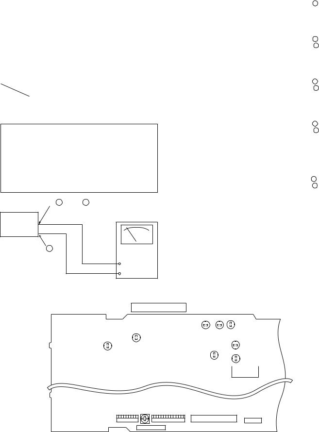
REMOVING AND REINSTALLING THE MAIN PARTS
CD MECHANISM SECTION
For the procedure to remove the CD mechanism from the main unit, refer to Disassembling Procedure, Steps 1~10, and 19. (p.8).
How to Remove the optical pickup (See Fig. 11-1.)
1.Remove the screws (A1)x 2 pcs., to remove shaft (A2)x 1 pc.
2.Remove stop washer (A3)x 1 pc., to remove gear (A4)x 1 pc.
3.Remove the optical pickup.
Note:
After disconnecting the optical pickup connector wrap the front end of connector in conductive aluminum foil so as to prevent damage to the optical pickup by static electricity.
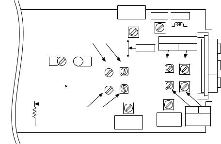
How to Remove the tray motor/main cam motor (See Fig. 11-2.)
1.Remove the CD changer section by the method described in page 8, and disassemble as shown in the figure.
2.Remove the belts (B1)x 2 pcs., from the motor side.
3.Remove the screws (B2)x 4 pc.
4.Remove the tray motor and main cam motor.
How to remove the CD disc (When CD is in playback state) (See Fig. 11-3.)
1.Remove the Top cabinet .
2.Disassemble as shown in the figure so that the CD disc of CD changer becomes visible.
3.Remove the CD disc as shown in the figure.
How to remove the CD disc (When CD exists in the tray) (See Fig. 11-4.)
1.Remove the Top cabinet.
2.Disassemble as shown in the figure so that the CD disc of CD changer can be taken out.
3.Remove the CD disc from the tray as shown in the figure.
(A1) x2 ø2.6 x5mm
Stop Washer (A3) x1
Pickup
CD
Mechanism
Shaft Gear (A2) x1 (A4) x1
Figure 11-1
 (B2) x2

 ø2.6 x4mm (B2) x2

ø2.6 x4mm
Belt |
|
|
(B1) x1 |
Belt |
|
|
||
|
(B1) x1 |
|
|
Main Cam |
|
|
Motor |
|
|
Tray Motor |
|
|
Figure 11-2 |
|
|
Turn the main cam clockwise, |
|
|
and raise the CD mechanism |
|
|
and disc holder up to |
|
|
uppermost position. |
|
Disc Holder |
||
CD Disc |
CD Changer |
|
Block |
||
|
||
(When CD is in playback state.) |
|
Figure 11-3 |
|
|
Turn the main cam clockwise, |
|
and raise the CD mechanism |
|
and disc holder up to |
Disc Holder |
uppermost position. |
CD Mechanism |
CD Changer |
CD Disc |
|
|
Block |
1 |
Press in turns the arrow |
parts, starting with the |
|
2 |
uppermost one, to |
3 |
withdraw the disc trays |
Disc Tray 1 Disc Tray 3
Disc Tray 2
(When CD exists in the tray)
Figure 11-4
– 11 –
CD-C1W,CP-C1W
ADJUSTMENT
MECHANISM SECTION
• Driving Force Check
Torque Meter |
Specified Value |
|
|
Play: TW-2412 |
Tape 1: Over 80 g |
|
Tape 2: Over 80 g |
|
|
• Torque Check
Torque Meter |
Specified Value |
|
|
|
|
|
Tape 1 |
Tape 2 |
|
|
|
Play: TW-2111 |
30 to 60 g. cm |
30 to 60 g.cm |
|
|
|
Fast forward: TW-2231 |
60 to 120 g.cm |
60 to 120 g.cm |
|
|
|
Rewind: TW-2231 |
60 to 120 g.cm |
60 to 120 g.cm |
|
|
|
• Tape Speed
|
Test Tape |
Adjusting |
Specified |
Instrument |
|
|
Point |
Value |
Connection |
Normal |
MTT-111 |
VRM01 |
3,000 ± |
Speaker |
speed |
|
|
30 Hz |
terminal |
|
|
|
|
|
TAPE SECTION
Position of each switch or control
Volume |
MAX |
|
|
3D Surround Mode Button |
PASS |
|
|
Pre-programmed Equalizer |
FLAT |
|
|
Extra Bass |
OFF |
|
|
Function |
TAPE |
|
|
Dolby NR switch |
OFF |
|
|
X-Bass |
OFF |
|
|
RECORD |
TP490 2 PIN OR 4 PIN |
MODE |
ELECTRONIC |
|
|
UNIT |
VOLTMETER |
|
|
|
TP490 3 PIN |
|
GND |
|
Figure 12-1 BIAS CURRENT |
• Bias Frequency
Adjusting Point |
Specified Value |
Instrument |
|
Connection |
|||
|
|
||
— |
98 ± 10 kHz |
CNP102 1 |
|
|
|
|
• Bias Current
Adjusting Point |
Specified Value |
Instrument |
||
Connection |
||||
|
|
|||
|
|
|
|
|
L: VR101 |
Normal: 45 ± 10 mV |
L: TP490 |
4 |
|
R: VR102 |
CrO2: 65 ± 15 mV |
R: TP490 |
2 |
|
|
|
|
|
|
• Tape 1 Playback Amplifier Sensitivity
Test Tape |
Adjusting |
Specified Value |
Instrument |
||
Point |
Connection |
||||
|
|
||||
|
|
|
|
|
|
MTT-150 |
L: VRD01 |
Normal: 300 mV |
L: TP451 |
3 |
|
R: VRD02 |
R: TP451 |
1 |
|||
|
|
||||
|
|
|
|
|
|
• Tape 2 Playback Amplifier Sensitivity
Test Tape |
Adjusting |
Specified Value |
Instrument |
||
Point |
Connection |
||||
|
|
||||
|
|
|
|
|
|
MTT-150 |
L: VRD03 |
Normal: 300 mV |
L: TP451 |
3 |
|
R: VRD04 |
R: TP451 |
1 |
|||
|
|
||||
|
|
|
|
|
|
• Record/Playback Sensitivity
Test Tape |
Adjusting |
Specified Value |
Instrument |
||
Point |
Connection |
||||
|
|
||||
|
Record level |
215 mV |
Input: VIDEO |
||
|
control |
Ouyput: |
|
||
UR-127 |
|
|
|||
|
|
L: TP451 |
3 |
||
L: VR151 |
215 mV |
||||
|
|||||
|
R: TP451 |
1 |
|||
|
R: VR152 |
||||
|
|
|
|
||
|
|
|
|
|
|
MAIN PWB
|
|
|
|
|
|
|
|
|
|
|
|
|
VR152 VRD02VRD04 |
||||||||||||||||||||
|
|
|
|
|
|
|
|
|
|
|
|
R-CH REC/ |
|
|
|
|
|
|
|
|
|
|
|
|
|
|
|
TAPE2 PLAY |
|
|
|||
|
|
|
|
|
|
|
VR101 |
PLAY SENS. |
|
|
|
|
|
|
|
|
|
|
|
|
|
|
|
R-CH SENS. |
|
|
|||||||
|
|
|
|
|
|
|
|
|
|
|
|
|
|
|
|
|
|
|
|
|
|
|
|
|
|
|
|
|
|||||
|
|
|
|
|
|
TP490 |
|
|
|
|
|
|
|
TAPE1 PLAY |
|
|
|
|
|
|
|
|
|
|
|
||||||||
VR102 |
|
|
|
|
|
|
|
|
R-CH SENS. |
|
|
VRD03 |
|
|
|
|
|
|
|||||||||||||||
|
|
|
|
|
|
1 2 3 4 |
|
|
|
|
|
|
|
|
|
|
|
|
|
|
|
|
|
|
|
|
|
|
TAPE2 PLAY |
|
|||
|
|
|
|
|
|
|
|
|
|
|
|
|
|
|
|
|
|
|
|
|
|
|
|
|
|
|
|
|
|
||||
|
|
|
|
|
|
|
L-CH BIAS |
|
|
|
|
VR151 |
|
|
|
|
|
L-CH SENS. |
|
||||||||||||||
|
|
|
|
|
|
|
|
|
VRD01 |
||||||||||||||||||||||||
|
|
|
|
|
|
|
CURRENT |
|
|
|
|
|
|
|
|
|
|
|
|
|
|
|
|
|
|
|
|
||||||
R-CH BIAS |
|
|
|
|
|
|
|
|
|
|
|
|
|
|
|
|
TP451 |
||||||||||||||||
CURRENT |
|
|
|
|
|
|
|
|
|
L-CH REC/ |
|
|
|
|
|
|
|
|
|
1 2 3 |
|||||||||||||
|
|
|
|
|
|
|
|
|
|
|
|
|
|
|
|
|
|
|
|
|
|
|
|
|
|
||||||||
|
|
|
|
|
|
|
|
|
|
|
|
|
|
PLAY SENS. |
|
|
|
TAPE1 PLAY |
|||||||||||||||
|
|
|
|
|
|
|
|
|
|
|
|
|
|
|
|
|
|
|
|
|
|
|
|
|
L-CH SENS. |
||||||||
|
WTM1 VRM01 WTM2 |
CFW2 |
|
|
|
||
|
|
||
|
|
CNP851
TAPE SPEED
Figure 12-2 ADJUSTMENT POINTS
– 12 –
TUNER SECTION
fL: Low-range frequency fH: High-renge frequency
• AM IF/RF
Signal generator: 400 Hz, 30%, AM modulated
Test Stage |
Frequency |
Frequency |
Setting/ |
Instrument |
|
|
Display |
Adjusting |
Connection |
|
|
|
Parts |
|
|
|
|
|
|
IF |
450 kHz |
1,602 kHz |
T351 |
*1 |
|
|
|
|
|
MW Band |
— |
531 kHz |
(fL): T306 |
*2 |
Coverage |
|
|
1.1 ± 0.1 V |
|
|
|
|
|
|
SW1 Band |
— |
3.2 MHz |
(fL): T307 |
*2 |
Coverage |
|
|
2.0 ± 0.1V |
|
|
|
|
|
|
SW1 Band |
— |
7.3 MHz |
(fH): TC305 |
*2 |
Coverage |
|
|
7.7 ± 0.2 V |
|
|
|
|
|
|
SW2 Band |
— |
9.5 MHz |
(fL): T308 |
*2 |
Coverage |
|
|
2.1 ± 0.1V |
|
|
|
|
|
|
SW2 Band |
— |
21.85 MHz |
(fH): TC304 |
*2 |
Coverage |
|
|
7.7 ± 0.2V |
|
|
|
|
|
|
MW |
990 kHz |
990 kHz |
T302 |
*1 |
Tracking |
|
|
|
|
|
|
|
|
|
SW1 |
3.9 MHz |
3.9 MHz |
(fL): T303 |
*1 |
Tracking |
|
|
|
|
|
|
|
|
|
SW1 |
7.1 MHz |
7.1 MHz |
(fH): TC303 |
*1 |
Tracking |
|
|
|
|
|
|
|
|
|
SW2 |
11.65 MHz |
11.65 MHz |
(fL): T304 |
*1 |
Tracking |
|
|
|
|
|
|
|
|
|
SW2 |
21.45 MHz |
21.45 MHz |
(fH): TC302 |
*1 |
Tracking |
|
|
|
|
|
|
|
|
|
*1. Input: Antenna, |
Output: TP302 |
|
|
|
|
|
|
|
|
|
|
|
|
|
|
|
|
|
|
|
|
|
|||||
*2. Input: Anetnna, |
Output: TP301 |
|
|
|
|
|
|
|
|
|
|
|
|
|
|
|
|
|
|
|
|
|
|||||
• FM RF |
|
|
|
|
|
|
|
|
|
|
|
|
|
|
|
|
|
|
|
|
|
|
|
|
|
|
|
Signal generator: 1 kHz, 40 kHz dev, FM modulated |
|
|
|
|
|
||||||||||||||||||||||
|
|
|
|
|
|
|
|
|
|
|
|
|
|
|
|
|
|
|
|
|
|
|
|
|
|
|
|
Test Stage |
Frequency |
Frequency |
|
Setting/ |
|
|
|
|
|
Instrument |
|
||||||||||||||||
|
|
|
Display |
|
Adjusting |
Connection |
|
||||||||||||||||||||
|
|
|
|
|
|
|
|
Parts |
|
|
|
|
|
|
|
|
|
|
|
|
|
|
|
|
|||
Band |
— |
|
87.5 kHz |
(fL): LT02 |
|
|
|
|
*1 |
|
|
|
|
|
|
|
|||||||||||
Coverage |
|
|
|
|
|
|
3.7 ± 0.1 V |
|
|
|
|
|
|
|
|
|
|
|
|
||||||||
|
|
|
|
|
|
|
|
|
|
|
|
|
|
|
|
|
|
|
|
|
|
|
|
|
|
|
|
RF |
98 MHz |
|
98 MHz |
LT01 |
|
|
|
|
*2 |
|
|
|
|
|
|
|
|||||||||||
|
10 - 30 dB |
|
|
|
|
|
|
|
|
|
|
|
|
|
|
|
|
|
|
|
|
|
|
|
|
|
|
*1. Input: Antenna, |
Output: TP301 |
|
|
|
|
|
|
|
|
|
|
|
|
|
|
|
|
|
|
|
|
|
|||||
*2. Input: Anetnna, |
Output: Speaker Terminal |
|
|
|
|
|
|||||||||||||||||||||
|
|
|
|
|
|
|
|
|
|
|
|
|
|
|
|
|
|
|
|
|
|||||||
|
|
|
|
|
|
TUNER PWB |
|
|
|
|
|
|
|||||||||||||||
|
|
|
|
|
|
|
|
|
|
|
|
|
|
|
|
|
|
|
|
|
|
|
|
|
|
|
|
|
|
|
|
|
|
|
|
|
|
|
|
|
|
|
|
|
|
|
|
|
|
|
|
||||
|
|
|
|
|
|
|
|
|
|
|
|
|
|
|
|
|
|
|
|
SW1 Band |
|||||||
|
|
|
|
|
|
|
|
|
|
|
|
|
|
|
|
|
|
|
|
Coverage |
|||||||
|
|
|
|
|
|
|
|
|
|
|
|
|
|
|
|
|
|
|
|
fL |
|
|
fH |
||||
|
|
|
|
|
|
|
|
T351 |
VR351 |
|
|
|
|
|
|||||||||||||
|
|
|
|
|
|
|
|
|
|
|
|
|
|
|
|
|
|
|
|
|
|
|
|
T307 |
|||
|
|
|
|
|
|
|
|
|
|
|
|
|
|
|
|
|
|
|
|
|
|
|
|
||||
|
|
|
|
|
|
|
|
AM IF |
|
|
|
|
|
|
|
|
|
|
|
||||||||
|
|
|
|
|
|
|
|
|
|
FM Mute |
|
|
|
|
|
||||||||||||
|
|
|
|
|
|
|
|
|
|
|
|
Level |
|
|
|
|
|
||||||||||
|
|
|
|
|
|
|
|
|
|
|
|
|
T308 |
||||||||||||||
|
|
|
|
|
|
|
|
|
|
|
|
|
|
|
|
|
|
|
|
|
|
|
|
||||
|
|
|
|
|
|
IC303 |
|
|
|
|
|
|
|
|
|
|
|
|
|
|
|
|
|
||||
|
|
|
|
|
|
|
|
|
|
|
|
|
|
|
|
|
|
|
|
|
|
|
|
|
|
||
|
|
|
|
|
|
|
|
|
|
|
|
|
|
|
|
|
|
|
|
|
|
|
|
|
|
|
|
|
|
|
|
|
|
|
|
|
|
|
|
|
|
|
|
|
|
|
|
|
|
|
|
|
|
|
|
|
|
|
|
|
|
|
TP302 |
|
|
|
|
|
|
|
|
|
|
|
|
|
|
|
|
|
|
||
|
|
|
|
|
|
|
|
|
|
|
|
|
|
|
|
|
|
|
|
|
|
|
|
|
|
||
|
|
|
R357 |
|
|
|
|
|
|
|
|
|
|
|
|
fH |
|
fL |
|
||||||||
|
|
|
|
|
|
|
|
|
|
|
|
|
|
|
SW1 |
|
|
|
|
|
|||||||
|
|
|
|
|
|
|
|
|
|
|
|
|
|
|
|
|
|
|
|
|
|
|
|
||||
|
|
|
|
|
|
|
|
|
|
|
|
|
|
|
|
|
|
|
Tracking |
|
|||||||
|
|
|
|
|
|
|
|
|
|
|
|
|
|
|
|
|
|
|
|
|
|
|
|
|
|
|
|
CD-C1W,CP-C1W
• Setting the Test Mode
Keeping the PAUSE button and TUNER button pressed, turn on POWER. Then, the frequency is initially set in the memory as shown in Table. Call it with the PRESET button to use it for adjustment and check of tuner circuit.
Preset |
|
FM |
Preset |
MW |
Preset |
SW1 |
Preset |
SW2 |
|
||||
No. |
|
|
|
|
No. |
|
No. |
|
|
No. |
|
|
|
|
|
|
|
|
|
|
|
|
|
|
|
|
|
1 |
87.50 |
MHz |
6 |
531 kHz |
11 |
3.2 |
MHz |
16 |
9.5 |
MHz |
|
||
2 |
108.00 |
MHz |
7 |
1,602 kHz |
12 |
7.3 |
MHz |
17 |
21.85MHz |
|
|||
3 |
90.00 |
MHz |
8 |
603 kHz |
13 |
3.9 |
MHz |
18 |
11.65 |
MHz |
|
||
4 |
106.00 |
MHz |
9 |
1,404 kHz |
14 |
7.1 |
MHz |
19 |
21.45 |
MHz |
|
||
5 |
98.00 |
MHz |
10 |
990 kHz |
15 |
5.06 |
MHz |
20 |
15.1 |
MHz |
|
||
|
|
|
|
|
|
|
|
|
|
|
|
|
|
21 ~ 40 |
|
|
|
|
|
|
|
|
|
|
|
|
|
|
|
|
|
|
|
|
|
|
|
|
|
|
|
|
|
|
|
|
|
|
|
|
|
|
|
|
|
|
|
|
|
|
|
|
|
|
|
|
|
|
|
• FM Detection
Signal generator: 10.7 MHz, FM sweep
Test Stage |
Frequency |
Frequency |
|
Setting/ |
Instrument |
|
|
|
|
Display |
|
Adjusting |
Connection |
|
|
|
|
|
Parts |
|
IF |
10.7 MHz |
|
98 MHz |
|
TT01 |
*1 |
|
|
|
|
|
(Turn the |
|
|
|
|
|
|
core of trans- |
|
|
|
|
|
|
former TT01 |
|
|
|
|
|
|
fully counter- |
|
|
|
|
|
|
clock wise) |
|
|
|
|
|
|
|
|
*1. Input: Antenna, |
Output: TP301 |
|
|
|||
*2. Input: Anetnna, |
Output: Speaker Terminal |
|
||||
• FM Mute Level
Signal generator: 1kHz, 40 kHz dev., FM modulated
Frequency |
Frequency |
Adjusting |
Instrument |
|
Display |
Parts |
Connection |
|
|
|
|
98.00 MHz |
98.00 MHz |
VR351 *1 |
Input: Antenna |
(25 dBμV) |
|
|
Output: Speaker |
|
|
|
Terminal |
|
|
|
|
*1. Adjust so that an output signal appears.
FM Band
Coverage FM IF 
 FM RF
FM RF
LT02 |
|
TT01 |
LT01 |
|
|
SW2 Tracking |
|
|||
TP301 |
fH |
|
fL |
SO301 |
|
|
|
|
|
||
|
TC302 T304 |
ANTENNA |
|||
TC305 |
TERMINAL |
||||
|
|
|
|||
TC304 |
TC303 |
T303 |
|
||
|
|
|
|
||
T306 |
T302 |
|
|
|
|
|
|
|
|
||
|
|
|
fH fL |
|
|
MW Band |
MW |
|
SW1 |
|
|
Tracking |
Tracking |
|
|||
Coverage |
|
||||
|
|
|
|
||
Figure 13 ADJUSTMENT POINTS
– 13 –
CD-C1W,CP-C1W
TEST MODE
• Setting the test mode
Any one of test mode can be set by pressing several keys as follows.
Hold down the EQ and CD buttons, and press the POWER switch. TEST: CD operation test
• TEST mode
Function — CD test mode
Setting of TEST mode
Indication of CD TEST mode (Fig. 14-1) |
|
|
|
|
IL is not performed. |
|
|
||||||||
|
OPEN/CLOSE operation is manual operation. |
|
|
|
|
|
|||||||||
|
|
|
|
|
|
|
|
|
|||||||
|
|
|
|
|
) or ( |
) key. |
|
|
|
|
|
|
|||
The pickup can be moved by using the ( |
|
|
|
|
|||||||||||
|
|
|
|
|
|||||||||||
|
|
<MEMORY> |
|
When the track- |
|
Press the |
|
The pickup |
|
<MEMORY> |
|
When the track- |
|||
|
|
|
|
||||||||||||
|
|
|
|
||||||||||||
|
|
key input |
|
ing servo is acti- |
STOP button. willreturn to |
|
key input |
|
ing servo is acti- |
||||||
|
|
|
|
|
vated, playback |
|
|
the STOP |
|
|
|
vated, playback |
|||
|
|
|
|
|
|
|
|
|
|
||||||
|
|
|
|
|
will begin at the |
|
|
position. |
|
|
|
will begin at the |
|||
|
|
|
|
|
current position. |
|
|
|
|
|
|
|
|
current position. |
|
|
|
|
|
|
|
|
|
|
|
|
|
|
|
|
|
<STOP> |
|
The pickup nor- |
|
||
key input |
mally returns to |
|
|
|
the STOP posi- |
|
|
tion. |
<PLAY> key input
Note:
TOC. IL is performed, and the ordinary PLAY is performed. |
Press <STOP> key. |
Stop |
|
|
|
||
If the following key is pressed during PLAY, it is possible |
|
|
|
|
|
|
|
to specify directly any Track No. |
G9 |
G10 |
G9 |
G6 |
G5 |
G4 |
|
<Disc Number 1> key: Track 4 |
|||||||
|
|
|
|
|
|
||
<Disc Number 2> key: Track 9 |
|
|
|
|
|
|
|
<Disc Number 3> key: Track 15 |
G2 |
G3 G7 |
|
G8 |
|
|
|
|
|
|
|
|
|
||
Only in STOP state it is possible to slide the pickup with the ( ) or (
 ) key.
VOL. --- Last memory BAL. --- CENTER
G1 |
G2 |
G3 |
G4 |
G5 |
G6 |
G7 |
G8 |
G9 |
R.GEQ. --- FLAT
X-BAS --- OFF
Canceling method - POWER OFF
G1~G8 |
|
|
|
G10 |
|
|
S41 |
|
|
|
|
|
|
|
|
|
|
|
|
||
|
S20 |
|
|
|
|
|
|
|
||
S21 |
|
|
|
|
|
|
|
|||
S19 |
S18 |
|
|
|
S39 |
|
|
|
|
|
|
S17 |
|
|
|
|
S36 |
S37 |
S35 |
|
|
S14 |
|
|
S40 |
|
S33 |
S38 |
||||
|
|
S34 |
|
|
|
|||||
|
|
|
|
|
|
|||||
S16 S15 |
S13 S12 |
|
S31 |
|
S32 |
|
|
S30 |
||
S10 |
|
|
|
|
|
|
|
|
|
|
S9 |
S8 |
|
|
S29 |
|
|
|
S26 |
S28 |
|
|
S4 |
|
S3 |
|
S27 |
S25 |
S23 |
S24 |
|
|
|
|
|
|
|
|
|||||
S6 S5 |
|
|
|
|
|
|
|
|
|
|
S7 |
|
|
S1 |
|
|
|
S22 |
|
|
|
S2 |
|
|
|
|
|
|
|
|
|
|
|
|
|
|
|
|
|
|
|
|
|
CD SECTION
Figure 14 -1
Since this CD system incorporates the following automatic adjustment function, when the pickup is replaced, it is not necessary to readjust it.
Since this CD unit does not need adjustment, the combination of PWB and laser pickup unit is not restricted.
• Automatic adjustment item
1.Focus offset (Fig. 14-2)
2.Tracking offset (Fig. 14-3)
3.E/F balance (tracking error balance) (Fig. 14-4)
4.RF level AGC function (HF level: constant)
5.RF level automatic follow-up of the tracking gain
This automatic adjustment is performed each time a disc is changed. Therefore, each disc is played back using the optimal settings.
0.1s |
|
|
0.50 V |
|
|
IC1 16 |
FD |
|
|
|
FOCUS |
|
|
OFF-SET |
|
|
ADJUST |
0.1s |
|
|
0.50 V |
|
|
IC1 7 |
TE |
TRACKING |
|
|
|
|
|
OFF-SET |
|
|
1 ADJUST |
|
2 |
|
|
Figure 14-2 |
|
200 ms |
TRACKING/ |
|
1V/diV |
ERROR |
|
IC 1 15 |
BARANCE |
|
TO |
1 ADJUST |
|
|
||
200 ms |
|
|
1V/diV |
|
|
IC 1 7 |
2 |
|
TE |
||
|
||
|
Figure 14-4 |
10ms 0.50 V
IC1 16 FD
10ms 0.50 V IC1 7 TE
Figure 14-3
Enlarged
View
TRACKING
OFF-SET 1 ADJUST
2
– 14 –
CD-C1W,CP-C1W
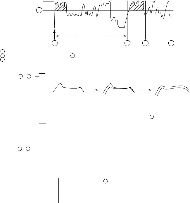
EXPLANATION OF AUTOMATIC SOUND VALUE CORRECTION CONTROL
1.Outline
The recent trend is toward rise of CD record level in the world, for example rock, dancing music, etc. In case of continuous high level playback G-EQ (graphic equalizer) and VOL (Volume) are controlled (lowered) automatically after a lapse of specific time (10 minutes) so as to get the easy-to-listen sound level.
2.Explanation of operation
The CD playback operation is explained below.
Distortion clip point
X |
SP output |
|
level |
0w
10 minutes
A B C D
X : Threshold value of control circuit operation
A: Hight energy (hatched area) exceeding X is detecated, and the control mode is set.
B: After a lapse of 10 minutes the control is started.
B ~ C :
Data is fetched every 4 seconds to control.
Initial frequency |
Hand L frequency char- |
VOL (Volume) is lowered. |
characteristics. |
acteristics are lowered. |
|
At first, the H and L frequency characteristics are lowered as shown above so thet the distortion and disturbance are reduced. However, if hight energy exceeding X is detected, VOL is lowered to get sound easy to listen.
C ~ D : |
|
|
Stable control |
|
|
|
|
|
|||
|
|
|
|
|
|
|
|||||
|
|
|
Continued control |
|
|
|
|
|
|||
|
|
|
The output data is fetched every |
4 seconds to control. When quiet music is played back, the |
|||||||
|
|
|
control is performed so as to restore the initial frequency characteristics and initial VOL values. |
||||||||
|
|
|
|
|
|
When output exceeding |
X is not given |
|
|
|
When quiet music is played back. |
Control mode cancel conditions |
|
|
|
|
|
||||||
|
|
|
|
|
|||||||
|
|
|
|||||||||
|
|
|
|
|
|||||||
|
|
continuously for 10 minutes. |
|
|
When VOL is lowered. |
||||||
|
|
||||||||||
|
|
|
|
|
|
|
|
|
|
|
|
When the power is turned off or on.
– 15 –
CD-C1W,CP-C1W
NOTES ON SCHEMATIC DIAGRAM
• Resistor:
To differentiate the units of resistors, such symbol as K and M are used: the symbol K means 1000 ohm and the symbol M means 1000 kohm and the resistor without any symbol is ohm-type resistor. Besides, the one with “Fusible” is a fuse type.
• Capacitor:
To indicate the unit of capacitor, a symbol P is used: this symbol P means micro-micro-farad and the unit of the capacitor without such a symbol is microfarad. As to electrolytic capacitor, the expression “capacitance/withstand voltage” is used.
(CH), (TH), (RH), (UJ): Temperature compensation (ML): Mylar type
(P.P.): Polypropylene type
•Schematic diagram and Wiring Side of P.W.Board for this model are subject to change for improvement without prior notice.
REF. NO |
DESCRIPTION |
POSITION |
|
|
|
SW202 |
SPAN SELECTOR |
50/9 |
|
|
|
SW701 |
VOLUME UP/DOWN |
OFF |
|
|
|
SW702 |
JOG DIAL |
OFF |
|
|
|
SW702A |
PICKUP IN |
OFF |
|
|
|
SW703 |
X-BASS |
OFF |
|
|
|
SW704 |
EQUALIZER/DEMO |
OFF |
|
|
|
SW705 |
SRS MODE |
OFF |
|
|
|
SW706 |
SRS PASS |
OFF |
|
|
|
SW707 |
FF |
OFF |
|
|
|
SW708 |
STOP |
OFF |
|
|
|
SW709 |
EDIT NORMAL |
OFF |
|
|
|
SW710 |
EDIT HIGH |
OFF |
SW711 |
RECORD/PAUSE |
OFF |
|
|
|
SW712 |
FORWARD PLAY |
OFF |
|
|
|
SW713 |
DOLBY-NR |
OFF |
SW717 |
REWIND |
OFF |
|
|
|
SW718 |
CD PAUSE |
OFF |
|
|
|
SW719 |
REVERSE PLAY |
OFF |
|
|
|
SW720 |
REVERSE MODE |
OFF |
|
|
|
SW721 |
CLOCK |
OFF |
|
|
|
SW722 |
TIMER |
OFF |
|
|
|
SW723 |
SLEEP |
OFF |
|
|
|
SW724 |
VIDEO/AUX |
OFF |
|
|
|
SW725 |
TAPE 1/2 |
OFF |
|
|
|
•The indicated voltage in each section is the one measured by Digital Multimeter between such a section and the chassis with no signal given.
1.In the tuner section, ( ) indicates AM
< > indicates FM stereo
2.In the main section, a tape is being played back.
3.In the deck section, a tape is being played back. ( ) indicates the record state.
4.In the power section, a tape is being played back.
5.In the CD section, the CD is stopped.
•Parts marked with “ ” (
” ( 


 ) are important for maintaining the safety of the set. Be sure to replace these parts with specified ones for maintaining the safety and performance of the set.
REF. NO |
DESCRIPTION |
POSITION |
|
|
|
SW726 |
TUNER (BAND) |
OFF |
|
|
|
SW727 |
CD |
OFF |
|
|
|
SW732 |
CLEAR |
OFF |
|
|
|
SW733 |
MEMORY/SET |
OFF |
|
|
|
SW734 |
POWER ON/STAND-BY |
OFF |
|
|
|
SW739 |
DISC 3 OPEN/CLOSE |
OFF |
|
|
|
SW740 |
DISC 3 |
OFF |
|
|
|
SW741 |
DISC 2 OPEN/CLOSE |
OFF |
|
|
|
SW742 |
DISC 2 |
OFF |
|
|
|
SW743 |
DISC 1 OPEN/CLOSE |
OFF |
|
|
|
SW744 |
DISC 1 |
OFF |
|
|
|
SW851 |
VOLTAGE SELECTOR |
230V-240V |
|
|
|
SWB101,102 |
CAM1, 2 |
OFF |
|
|
|
SWB103,104 |
CAM3, 4 |
OFF |
|
|
|
SWB105 |
CD EJECT |
OFF |
|
|
|
SWB107 |
CD IN |
OFF |
|
|
|
SWB108 |
CD SET |
OFF |
|
|
|
SWE1 |
TAPE 2 SIDE A FP |
OFF |
|
|
|
SWE2 |
TAPE 2 PLAY |
OFF |
|
|
|
SWE3 |
TAPE 2 SIDE B FP |
OFF |
|
|
|
SWE4 |
TAPE 2 CrO2 |
OFF |
|
|
|
SWE7 |
TAPE 1 CrO2 |
OFF |
|
|
|
SWE9 |
TAPE 1 PLAY |
OFF |
|
|
|
FRONT |
2SC535 C |
FRONT |
3 |
FRONT VIEW |
|
2SC1845 |
|
|
|||
VIEW |
VIEW |
|
|
||
2SC2236 Y |
TOP |
2 |
|
||
|
|
|
|||
|
2SC2878 B |
|
VIEW |
|
|
|
|
1 |
|
|
|
|
2SC2878 A |
|
|
|
|
|
|
|
|
|
|
|
2SD468 C |
|
|
|
|
E C B |
KTA1266 GR |
B C E |
KTA1504 Y |
|
|
(S)(G)(D) |
KTA1270 Y |
(D)(G)(S) |
|
|
|
(1)(2)(3) |
KTA1271 Y |
(3)(2)(1) |
KTC3875 GR |
KDV147 C |
|
|
2SD2012 |
|
|
||
|
KTA1273 Y |
|
KV1236Z23 |
|
|
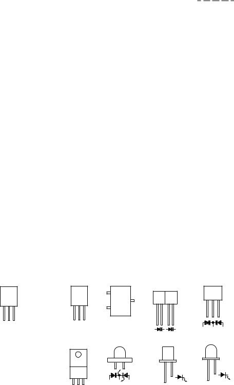
|
2SK2541 |
|
|
||
|
KTC3199 GR |
|
|
|
|
|
KTC3200 GR |
|
|
|
|
|
KTC3203 Y |
|
|
|
|
|
KRA107 M |
FRONT |
|
|
|
|
KRC102 M |
VIEW |
|
FRONT |
FRONT |
|
KRC104 M |
|
|
VIEW |
|
|
|
|
VIEW |
||
|
KRC107 M |
|
|
|
|
|
|
E C B |
SPR325MV |
484GT44 |
333GTH2 |
|
|
2SB1375 |
333GTH4 |
||
|
|
|
|
||
|
|
|
|
|
|
Figure 16 TYPES OF TRANSISTOR AND LED
– 16 –
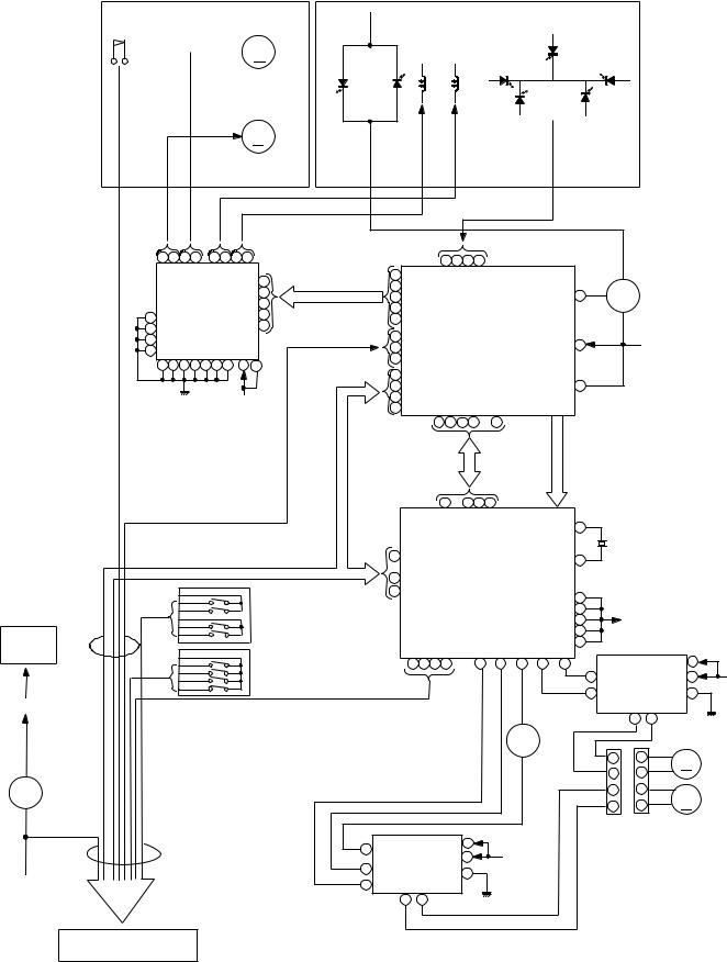
CD-C1W,CP-C1W
PICKUP IN
SW702A M702  M MOTORSLED
OPTICAL
PICKUP
IC1
IC2
+5V
Q81 VOLTAGE REGURATOR
+7.3V (B2)
M701
M SPINDLE
MOTOR
31 30 25 24 |
13 12 7 6 |
|
|||
SP+ |
SPSL- SL+ |
FO+ FO- |
TRTR+ |
1 |
|
|
IC3 |
|
|||
|
|
5 |
|||
|
M56748FP |
|
|||
|
|
14 |
|||
8 |
FOCUS/TRACKING/ |
22 |
|||
32 |
|||||
9 |
SPIN/SLIDE DRIVER |
||||
|
|||||
10 |
|
|
|
|
|
11 |
|
|
|
|
|
36 35 34 29 28 27 26 |
20 17 |
||||
|
|
|
+B1 |
SL+. SL–. DRF |
|
PU-IN SW |
|
|
|
||
CAM SWITCH
SWB101
SWB102
SWB103
SWB104
TRAY SWITCH
SWB105
SWB106
SWB107
SWB108
TO MAIN SECTION
TRACKING COIL |
FOCUS COIL |
OPTICAL PICKUP UNIT |
|
|
|
|
|
4 3 2 1 |
|
|
|
|
|
|
|
DRIVER |
|
|
||
|
|
|
|
|
F |
E FIN1 FIN2 |
|
|
|
|
|
|
|
|
|
||
|
|
15 TO |
|
|
|
|
|
|
|
|
|
|
|
LASER |
|
|
|
|
|
16 FD |
|
|
|
|
|
|
LD0 |
|
|
|
|
|
|
|
|
|
|
27 SPO |
|
|
|
|
|
62 |
|
|
Q1 |
|
|
|
|||
|
|
|
|
|
|
|
|
|
|
|
|
|
|||||
|
|
23 SP |
|
|
|
|
|
|
|
|
|
|
|
|
|
|
|
|
|
29 SLD |
|
IC1 |
|
|
|
|
|
|
|
|
|
|
|||
|
|
|
|
|
|
|
|
|
|
|
|
|
|
|
|
||
|
|
30 SL– |
|
|
LA9241M |
|
VCC1 |
64 |
|
|
|
+5V |
|
|
|||
|
|
31 |
SL+ |
|
SERVO AMP. |
|
|
|
|
|
|
||||||
|
|
|
|
|
|
|
|
|
|
|
|||||||
|
|
54 DRF |
|
|
|
|
|
|
|
|
|||||||
|
|
|
|
|
|
|
|
|
|
|
|
|
|
|
|||
|
|
50 CLK |
SLI SLC RFSM CV+ |
JP– |
|
|
VCC2 |
|
|
|
|
|
|
|
|||
|
|
51 CL |
|
|
|
56 |
|
|
|
|
|
|
|||||
CONTROL/CESELIAL |
|
52 DAT |
|
|
|
|
|
|
|
|
|
|
|
|
|
||
|
53 |
CE |
|
|
|
|
|
|
|
|
|
|
|
|
|
|
|
|
|
|
|
|
44 43 41 40 ~ 32 |
|
|
|
|
|
|
|
|
|
|
||
CL,DAT, |
|
|
|
|
JP– |
CLV+ EFMIN |
EFMO |
|
|
|
|
|
|
|
|
|
|
|
|
|
|
|
20 |
~ 12 10 |
9 |
|
|
|
|
|
|
|
|
|
|
|
|
|
COINCQCK.RES. WRQRWC.SQOUT. |
|
CONTROL |
|
XIN 45 |
|
|
|
|
|
|
||||
|
|
|
|
|
VDD 23 |
|
XL1 |
|
|
|
|||||||
|
|
53 |
|
|
|
|
|
|
|
|
|
|
16.934MHz |
|
|
||
|
|
|
|
|
IC2 |
|
|
XOUT 44 |
|
|
|
|
|
|
|||
|
|
~ |
|
|
|
|
|
|
|
|
|
|
|
||||
|
|
58 |
|
|
|
LC78622K |
|
|
|
|
|
|
|
|
|
||
|
|
61 |
|
|
SERVO SIGNAL VVDD 6 |
|
|
|
|
|
|
||||||
|
|
|
|
|
|
|
|
|
|
|
|
|
|
|
|
|
|
|
|
|
|
|
|
|
|
|
|
LVDD 36 |
|
|
+5V |
|
|
||
|
|
|
RCHO |
RVSS |
LVSS LCHO |
|
|
|
|
RVDD 41 |
|
|
|
|
|
|
|
|
|
|
|
|
|
|
XVDD 43 |
|
|
|
|
|
|
||||
|
|
|
|
|
|
|
|
|
|
|
|
|
|
|
|
||
|
|
|
40 39 38 37 |
26 |
27 |
28 |
24 |
25 |
|
|
|
IC82 |
2 |
|
|||
|
|
|
|
|
|
|
|
|
|
|
|
1 |
|
6 |
+B4 |
||
|
|
|
|
|
|
|
|
|
|
CONT2 |
|
TA7291S |
|||||
|
|
|
|
|
|
|
|
|
CONT1 |
|
9 |
TRAY MOTOR |
5 |
|
|||
|
|
|
|
|
|
|
|
|
|
|
|
DRIVER |
|
|
|||
|
|
|
|
|
|
|
|
|
|
|
|
|
|
3 |
7 |
|
|
|
|
|
|
|
|
|
|
Q51 |
|
|
|
|
|
|
|
|
|
|
|
|
|
|
|
|
|
|
|
|
|
|
4 |
|
4 |
M |
MOB2 |
|
|
|
|
|
|
|
|
SWITCHING DRIVER |
|
|
|
|
|
TRAY |
|||
|
|
CONT4 |
|
|
|
|
|
|
|
|
1 |
||||||
|
|
|
|
|
|
|
|
|
1 |
|
M |
MOTOR |
|||||
|
|
|
|
|
|
|
|
|
|
|
|
|
3 |
|
3 |
|
MOTOR |
|
|
CONT3 |
|
|
|
|
|
|
|
|
2 |
|
2 |
|
MOB1 |
||
|
|
|
|
|
|
|
|
|
|
|
|
|
|
MAIN CAM |
|||
|
|
|
|
|
|
|
|
|
|
|
|
|
|
|
|
|
|
|
|
CONT5 |
|
|
|
|
|
|
|
|
|
|
|
|
|
||
|
8 |
|
IC81 |
|
2 |
|
|
|
|
|
|
|
|
|
|
|
|
|
|
|
6 |
+B4 |
|
|
|
|
|
|
|
|
|
||||
|
1 |
|
TA7291S |
|
|
|
|
|
|
|
|
|
|||||
|
|
|
|
|
|
|
|
|
|
|
|
|
|
||||
|
MAIN CAM MOTOR 5 |
|
|
|
|
|
|
|
|
|
|
|
|||||
|
|
|
|
|
|
|
|
|
|
|
|
|
|||||
|
9 |
|
DRIVER |
|
|
|
|
|
|
|
|
|
|
|
|
||
|
|
|
3 |
7 |
|
|
|
|
|
|
|
|
|
|
|
|
|
Figure 17 BLOCK DIAGRAM (1/3)
– 17 –
CD-C1W,CP-C1W |
|
|
|
|
|
|
|
|
|
|
|
|
|
|
|
|
|
|
|
|
|
|
|
|
|
|
|
|
|
|
|
|
|
|
|
|
|
|
|
|
||||
|
FM BAND |
|
|
|
|
|
|
|
|
|
|
|
|
|
|
|
|
|
|
|
|
|
|
|
FM IF CF351 |
+B7 |
|
456KHz |
|
|
|
|
|
|
|
|
|
|
|
|
||||
|
PASS FILTER |
|
|
|
|
|
|
|
|
|
|
|
|
|
|
|
|
+B7 |
|
|
|
|
|
|
X351 |
|
|
|
|
|
|
|
|
|
|
|
|
|||||||
SO301 |
|
|
|
|
|
|
|
|
|
|
|
|
|
|
|
|
|
|
|
|
|
|
|
|
|
|
|
|
|
|
|
|
|
|
|
|
|
|||||||
ANTENNA |
BFT01 |
|
|
|
|
|
|
|
|
|
|
|
|
|
|
|
|
|
|
|
|
|
|
|
|
|
|
|
|
|
|
|
|
|
|
|
||||||||
TERMINAL |
2 |
3 |
|
|
|
ICT01 |
|
|
|
FM IF |
|
|
FM IF |
|
|
|
|
|
|
|
|
|
|
|
|
|
|
|
|
|
|
|
|
|
|
|
|
|
|
|
|
|||
FM |
1 |
|
|
|
|
|
|
|
|
|
|
|
|
|
|
|
|
|
|
|
|
|
|
|
|
|
|
|
|
|
|
|
|
|
|
|
|
|
|
|||||
|
|
|
|
1 |
|
TA7358AP |
6 |
|
TT01 |
|
|
CF302 |
|
AM IF |
|
|
AM IF |
|
|
|
|
|
|
|
|
|
|
|
|
|
|
|
|
|
|
|
|
|||||||
|
|
|
|
|
|
|
|
|
|
|
|
|
|
|
|
|
|
|
|
|
|
|
|
|
|
|
|
|
|
|
|
|||||||||||||
GND |
|
|
|
|
|
FM FRONT END |
|
|
|
|
|
|
|
|
T351 |
|
CF352 |
|
|
|
|
|
|
|
|
|
|
|
|
|
|
|
|
|
|
|
|
|||||||
SW1 |
|
|
|
|
|
|
3 |
|
8 |
9 |
|
|
|
|
FM IF IN |
|
|
|
|
|
|
|
|
|
|
|
|
|
|
|
|
|
|
|
|
|
|
|
|
|
|
|
|
|
|
|
|
|
5 |
|
|
7 |
|
|
|
|
|
|
|
|
|
|
|
|
|
|
|
|
|
|
|
|
|
|
|
|
|
|
|
|
|
|
|
|
|
||||
SW2 |
|
|
|
|
|
|
|
|
|
|
|
|
1 |
2 |
|
3 |
|
|
|
|
4 |
|
5 |
8 |
9 |
|
|
|
|
|
|
|
|
|
|
|
|
|
|
|
||||
|
|
|
|
|
|
FM RF |
|
FM OSC |
|
|
|
|
|
|
|
|
|
|
|
|
|
17 |
|
18 |
16 |
|
|
|
|
|
|
|
|
|
|
|||||||||
MW |
|
|
|
|
|
|
|
|
|
|
|
|
|
|
|
OUT |
|
REG |
|
|
IN |
GND |
|
VCC |
|
|
OUT |
IN IC303 |
|
|
|
|
|
|
|
|
||||||||
|
|
|
|
|
|
|
LT01 |
|
LT02 |
AMP |
|
|
|
VR351 |
|
|
|
|
|
|
|
|
|
|
|
|
|
|
|
|||||||||||||||
|
|
|
|
|
|
|
|
|
|
|
|
|
|
|
|
|
|
|
|
|
|
|
|
|
|
|
|
|
LA1832 |
|
|
|
|
|
|
|
|
|||||||
|
|
|
|
|
|
|
|
|
|
|
|
|
|
|
|
|
|
|
|
|
|
|
|
|
|
|
|
|
|
|
|
|
|
|
|
|
|
|
|
|
||||
|
|
|
|
|
|
|
|
|
|
QT01 |
|
|
|
FM MUTE LEVEL |
|
|
|
|
|
|
|
|
|
IF |
|
|
|
|
|
|
|
|
FM IF DET./FM MPX./AM IF |
|
|
|
|
TUNER |
||||||
|
|
|
|
|
|
|
|
|
|
|
|
|
|
|
|
AM OSC |
|
|
|
|
|
|
|
|
|
|
|
|
|
SD |
|
|
|
|
||||||||||
|
|
|
|
|
|
|
|
|
|
|
|
|
|
|
|
|
|
|
|
|
|
OUT |
|
|
|
|
|
|
|
16 |
|
|
|
|
|
|
|
|
||||||
|
|
|
|
|
|
|
|
|
|
|
|
|
|
|
|
|
|
|
7 |
|
|
|
|
|
|
|
|
|
|
|
|
|
|
|
|
|
|
|||||||
|
|
|
|
|
|
|
|
|
|
|
|
|
|
|
|
|
24 |
23 |
22 |
21 |
|
13 |
10 |
|
|
12 |
|
|
14 15 |
|
|
|
|
|
|
|
|
|
|
|||||
|
|
|
|
|
|
|
|
|
|
|
|
|
|
|
|
|
OUT |
IN |
AFC |
AM RF IN |
STEREO |
MONO/ST |
|
|
|
|
|
|
|
|
|
L |
R |
|
|
|
|
|
|
|
|
|
|
|
|
|
|
|
|
|
|
|
|
|
|
|
|
FMOSC |
|
|
|
|
|
|
|
|
|
|
|
|
|
MUTING |
|
|
|
|
|
|
|
|
|||||||||
|
|
|
|
|
|
|
|
|
|
|
|
|
|
|
|
|
|
|
|
|
|
|
|
|
|
|
|
|
|
|
|
|
|
|
|
|||||||||
|
|
|
|
|
|
|
|
|
|
|
|
|
|
|
|
|
|
|
|
|
|
Q361 |
|
|
|
Q353 |
|
|
|
|
|
|
|
|
|
|||||||||
|
|
|
|
|
|
|
|
|
|
|
|
|
|
|
|
|
|
|
|
|
|
|
|
|
|
|
|
Q354 |
|
|
|
|
|
|
|
|
|
|||||||
|
|
|
|
|
|
|
|
|
|
|
|
|
|
|
|
|
|
|
|
|
|
|
|
|
|
|
|
|
|
|
|
|
|
|
|
|
|
|
|
|
|
|
|
|
|
|
|
|
|
|
SW1/SW2 |
|
SW1/SW2 |
|
|
|
|
|
|
|
|
|
|
|
|
|
|
|
|
|
|
|
|
|
|
|
|
|
|
IC502/IC503/IC504 |
|
|
|
|
|||||
|
|
|
|
|
|
ANT. |
|
OSC. |
|
|
|
|
|
|
|
|
AM IN |
|
|
|
|
|
|
|
|
|
|
|
|
|
|
|
|
|
NJM4558MF |
|
|
|
|
|
||||
|
|
|
|
|
|
|
|
|
|
|
|
|
|
|
|
|
|
|
|
|
|
|
|
|
|
|
|
|
|
|
|
|
|
|
|
|
|
|
|
|||||
T302 |
|
|
T306 |
|
T303 |
|
|
|
T307 |
|
|
|
|
|
|
|
|
|
|
|
|
|
|
|
|
|
VOLTAGE |
|
|
|
|
|
|
|
OPE AMP. |
|
|
|
|
|
||||
MW ANT. |
|
MW OSC. |
|
T304 |
|
|
|
T308 |
|
|
|
|
|
|
|
|
|
|
|
|
|
|
|
|
REGURATER |
|
|
|
|
|
|
|
|
|
|
|
|
|
|
S |
||||
|
|
|
|
|
|
|
|
|
|
|
|
|
|
|
|
|
|
|
|
|
|
|
|
|
|
|
+B7 |
|
|
|
|
|
|
|
|
2 |
|
|
1 |
|
|
|
||
|
|
|
|
|
|
|
|
|
|
|
|
|
|
|
|
|
|
|
|
|
|
|
FM MONO/ST |
|
|
|
|
|
|
|
|
|
|
|
|
|
|
|
|
|
|
|
||
|
|
|
|
|
|
|
|
|
|
|
|
|
|
|
|
|
|
|
|
|
|
|
|
|
|
|
|
|
|
|
|
|
|
|
+B8 |
8 |
B.P.F |
4 |
–B6 |
|
|
|
||
|
|
|
|
|
|
|
Q308 |
|
|
Q306 |
|
|
|
|
|
X352 |
|
|
AM IN |
|
FM IN |
|
|
|
|
|
|
|
|
|
|
|
|
|
|
6 |
|
|
7 |
|
|
|
TAPE M |
|
|
|
|
|
|
|
|
|
|
|
|
|
|
|
|
|
|
|
|
IF IN |
|
|
|
|
|
|
|
|
|
|
|
|
|
|
|
|
|
|
T1 SOL |
||||||
|
|
|
|
|
|
|
Q309 |
|
|
Q307 |
|
|
+B7 |
|
|
4.5MHz |
|
|
|
|
|
|
|
+12V |
|
|
|
|
|
|
|
|
|
|
|
|
|
|
||||||
|
|
|
|
|
|
|
|
|
|
|
|
|
|
|
|
|
|
|
|
|
|
|
|
|
|
|
|
|
|
|
|
|
|
|
|
|
|
|||||||
|
|
|
|
|
|
|
|
|
|
|
|
|
|
|
|
1 |
|
22 |
15 |
16 |
|
11 |
10 |
12 |
|
17 |
|
|
|
|
|
|
|
|
|
|
|
|
|
|
|
T |
||
|
|
|
|
|
|
|
|
|
|
|
|
|
|
|
FM |
|
|
|
|
|
|
|
|
|
|
|
|
|
|
|
|
|
|
T1 PLAY |
||||||||||
|
|
|
|
|
|
|
|
|
|
|
|
|
Q360 |
|
7 |
OSC |
|
IC302 |
|
|
|
|
|
|
|
|
|
|
|
|
|
|
|
|
|
|
|
|
||||||
|
|
|
|
|
|
|
|
|
|
|
|
|
|
|
|
|
|
|
|
|
|
|
|
|
|
|
|
|
|
|
|
|
|
|
HIGH |
|||||||||
|
|
|
|
|
|
|
|
|
|
|
|
FM +B |
Q361 |
|
|
|
|
|
|
|
|
|
|
|
|
|
|
|
|
|
|
IC502(1/2) |
|
|
|
|
||||||||
|
|
|
|
|
|
|
|
|
|
|
|
|
|
|
|
|
|
|
LC72131 |
|
|
|
|
|
|
|
|
|
|
|
|
|
|
|
|
|
T2 SOL |
|||||||
|
|
|
|
|
|
|
|
|
|
|
|
|
|
|
|
|
|
|
|
|
|
|
|
|
8 |
|
|
|
|
|
|
|
|
|
|
|
||||||||
|
|
|
|
|
|
|
|
|
|
|
|
|
|
|
|
20 |
|
PLL CONTROLLER |
|
|
|
|
|
|
|
|
|
|
|
|
|
|
8 |
+B8 |
|
|
T |
|||||||
|
|
|
|
|
|
|
|
|
|
|
|
|
+B7 |
|
|
|
|
|
|
|
|
|
|
|
|
|
|
|
|
|
|
|
|
|||||||||||
|
|
|
|
|
|
|
|
|
|
|
|
|
|
|
9 |
|
|
13 |
|
3 |
4 |
5 |
6 |
21 |
|
|
|
|
|
|
|
|
|
|
7 |
|
|
|
|
|
|
T2 PLAY |
||
|
|
|
|
|
|
|
|
|
|
|
|
|
|
|
|
|
|
|
|
|
|
|
|
|
|
|
|
|
|
|
6 |
|
|
|
||||||||||
|
|
|
|
|
|
|
|
|
|
|
|
|
|
|
|
|
|
|
|
|
CE |
DI |
CL |
DO |
|
|
|
|
|
|
|
|
|
|
|
|
|
|
|
|
|
|
T |
|
|
|
|
|
|
|
|
|
|
|
|
|
|
|
|
|
|
|
|
|
|
|
|
|
|
|
|
|
|
|
|
|
|
|
|
|
|
|
|
|
|||||
|
|
|
|
|
|
|
|
|
|
|
|
MW +B |
|
|
|
|
|
|
|
|
|
|
|
|
|
|
|
|
|
|
|
|
|
|
|
|
|
|
|
T |
||||
|
|
|
|
|
|
|
|
|
|
|
|
Q362 |
|
|
|
|
|
|
|
|
|
|
|
|
|
|
|
|
|
|
|
|
|
|
|
|
|
|
|
|
|
|
||
|
|
|
|
|
|
|
|
|
|
|
|
|
|
|
+B7 |
|
|
|
|
|
|
|
|
|
|
|
|
|
|
|
|
|
|
|
|
|
|
|
|
|
|
|
|
|
|
|
|
|
|
|
|
|
|
|
|
|
|
|
|
|
|
|
|
|
|
|
|
|
|
|
|
|
|
|
|
|
|
|
|
|
|
|
SPE IN |
|
|
|
|||
|
|
|
|
|
|
|
|
|
|
|
|
|
|
|
|
+B7 |
|
|
|
|
|
|
|
|
|
|
|
|
|
|
|
|
|
|
|
|
|
|
|
REC |
||||
|
|
|
|
|
|
|
|
|
|
|
|
|
|
|
|
|
|
|
|
|
|
|
|
|
|
|
|
|
|
|
|
|
|
|
|
|
|
|
|
|
|
|||
|
|
|
|
|
|
|
|
|
|
|
|
SW1 +B |
|
|
|
|
|
|
|
|
|
|
|
|
|
|
|
|
|
|
|
|
|
|
|
|
|
|
|
|
|
|
|
|
|
|
|
|
|
|
|
|
|
|
|
|
|
|
Q363 |
|
|
|
|
|
|
|
|
|
|
|
|
|
|
|
|
|
|
|
|
|
|
|
|
|
|
|
|
||
|
|
|
|
|
|
|
|
|
|
|
|
|
|
|
|
|
|
|
|
|
|
|
|
|
|
|
|
|
|
|
|
|
|
|
|
|
|
|
|
|
|
|
||
|
|
|
|
|
|
|
|
|
|
|
|
SW2 +B |
|
|
|
Q364 |
|
|
|
|
|
|
|
|
|
|
|
|
|
|
|
|
|
|
|
|
|
|
|
|
|
|
T |
|
|
|
|
|
|
|
|
|
|
|
|
|
|
|
|
|
|
|
|
|
|
|
|
|
|
|
|
|
|
|
|
|
|
|
|
|
|
|
|
|
|
|
R |
||
|
|
|
|
|
|
|
|
|
|
|
|
|
|
|
|
|
|
|
|
|
|
|
|
|
|
|
|
|
|
|
|
|
|
|
|
|
|
|
|
|
|
|
|
|
L-CH R-CH |
|
|
|
|
|
|
|
|
|
|
|
|
|
|
|
|
|
|
|
|
|
|
|
|
|
|
|
|
|
|
|
|
|
|
|
|
|
|
|
|
|
|
|
|
JT01 |
|
|
|
|
|
|
|
|
|
|
|
|
|
|
|
|
|
|
|
|
|
|
|
|
|
|
|
|
|
|
|
|
|
|
|
|
|
|
|
|
|
|
|
|
VIDEO/AUX |
|
|
|
|
|
|
|
|
|
|
|
|
|
|
|
|
|
|
|
|
|
|
|
|
|
|
|
|
|
|
|
|
|
|
|
|
|
|
|
|
|
|
|
|
INPUT |
|
|
|
|
|
|
|
|
|
|
|
|
|
|
|
|
|
|
|
|
|
|
|
|
|
|
|
|
|
|
|
|
|
|
|
|
|
|
|
|
|
|
|
|
|
|
|
|
|
+B7 |
|
|
|
|
|
|
|
|
|
|
|
|
|
|
|
|
|
|
|
|
|
|
|
|
|
|
|
|
|
|
|
|
|
|
|
|
|
|
|
|
|
|
|
OUT |
8 |
|
IN |
|
|
|
|
|
|
|
|
|
|
|
|
|
|
|
|
|
|
|
|
|
|
|
|
|
|
|
|
|
|
|
|
|
|
|
|
|
|
|
|
|
L 7 |
|
L |
|
|
|
|
|
|
|
|
|
|
|
|
|
|
|
|
|
|
|
|
|
|
|
|
|
|
|
|
|
|
|
|
|
|
|
|
|
|
|
|
|
|
|
5 |
|
|
|
|
|
|
|
|
|
|
|
|
|
|
|
|
|
|
|
|
|
|
|
|
|
|
|
|
|
|
|
|
|
|
|
|
|
||
|
|
|
|
R 1 |
4 |
3 |
R |
|
|
|
|
|
|
|
|
|
|
|
|
|
|
|
|
|
|
|
|
|
|
|
|
|
L251 |
MPX.FILTER |
|
|
|
|
|
|
|
|
||
|
|
|
|
ICT01 |
|
|
|
|
|
|
|
|
|
|
|
|
|
|
|
|
|
|
|
|
|
|
|
|
|
|
|
L252 |
|
|
|
|
|
|
|
|
||||
|
|
|
|
|
|
|
|
|
|
|
|
|
|
|
|
|
|
|
|
|
|
|
|
|
|
|
|
|
|
|
|
|
|
|
|
|
|
|
|
|
|
|||
JT02 |
|
|
NJM4558MF |
|
|
|
|
QM21 |
|
Q501 |
|
CD MUTE |
|
|
|
|
|
|
|
|
|
|
|
|
|
|
|
|
|
|
|
|
|
|
|
|
|
|
|
|
||||
|
|
|
LINE AMP |
–B6 |
|
|
|
|
|
|
|
|
|
|
|
|
|
|
|
|
|
|
|
|
|
|
|
|
|
|
|
|
|
|
|
|
|
|||||||
|
|
|
|
|
|
|
|
|
Q502 |
|
|
|
|
|
|
|
|
|
|
|
|
|
|
|
|
|
|
|
|
|
|
|
|
|
|
|
|
|
|
|
||||
LINE |
|
|
|
|
|
|
|
|
|
|
|
|
|
|
|
|
|
|
|
|
|
|
|
|
|
|
|
|
|
|
|
|
|
|
|
|
|
|
|
|
|
|
||
|
|
|
|
|
|
|
|
|
|
|
|
|
|
|
|
|
|
|
|
|
|
|
|
|
|
|
|
|
|
|
|
|
|
|
|
|
|
|
|
|
|
|
|
|
OUT |
|
|
|
|
|
|
|
|
|
|
|
|
|
|
|
|
|
|
|
|
|
|
|
|
|
|
|
|
|
|
|
|
|
|
|
|
|
|
|
|
|
|
|
|
L-CH |
R-CH |
|
|
|
|
|
|
|
|
|
|
|
|
|
|
|
|
|
|
|
|
|
|
|
|
|
|
|
|
|
|
|
|
|
|
|
|
|
|
|
|
|
|
|
|
|
|
|
|
|
|
|
|
|
|
|
|
|
|
|
|
|
|
|
|
|
|
|
|
|
|
|
|
|
|
|
|
|
|
|
|
|
|
14 30 |
|
|
|
|
|
FROM CD UNIT |
|
|
|
|
|
|
|
|
|
|
|
|
|
|
|
|
|
|
|
|
|
|
|
|
|
|
|
|
|
|
|
|
CD |
L 55 |
|
|
|
|
|
|
IC501 |
|||
|
+B6 |
|
|
|
|
|
|
|
|
|
|
|
|
|
|
|
|
|
|
|
|
|
|
|
|
|
|
|
|
|
|
|
|
R 57 |
|
|
|
|
LC75396N |
|||||
|
|
|
|
|
|
|
|
|
|
|
|
|
|
|
|
|
|
|
|
|
|
|
|
|
|
|
|
|
|
|
|
|
|
|
|
|
|
|
||||||
|
MM1 |
|
MOTOR |
|
|
|
|
|
|
|
|
|
|
|
|
|
|
|
|
|
|
|
|
|
|
|
|
|
|
|
|
|
TAPE |
L 53 |
|
|
|
AUDIO PROCE |
||||||
TAPE MOTOR |
|
DRIVER |
|
|
|
TAPE MOTOR |
T2 CrO2 |
|
|
|
|
|
|
|
|
|
|
|
|
|
|
|
|
|
|
|
|
|
|
|
|
R 59 |
|
|
|
|
|
GRAPHIC E |
||||||
|
M |
|
QM02 |
|
|
|
|
|
|
|
|
|
|
|
|
|
|
|
|
|
|
|
|
|
|
|
|
|
|
|
|
|
|
TUNER |
L 54 |
|
|
|
|
|
||||
|
|
|
|
|
|
|
|
|
|
|
|
|
|
|
|
|
|
|
|
|
|
|
|
|
|
|
|
|
|
|
|
|
|
|
|
|
|
|
|
|
||||
|
|
|
|
QM01 |
QM08 |
|
HI SPEED |
|
|
|
|
|
|
|
|
|
|
|
|
|
|
|
|
|
|
|
|
|
|
|
|
|
|
R 58 |
|
|
|
|
|
|
|
|
||
|
|
|
|
|
|
|
|
|
|
|
|
|
|
|
|
|
|
|
|
|
|
|
|
|
|
|
|
|
|
|
|
|
|
|
|
|
|
|
|
|||||
|
|
|
|
|
|
|
|
|
|
|
|
|
|
|
|
|
|
|
|
|
|
|
|
|
|
|
|
|
|
|
|
|
|
|
|
|
|
|
|
|
|
|||
PHM1/PHM2 |
|
|
DRIVER |
SWITCHING |
|
|
|
|
|
|
|
|
|
|
|
|
|
|
|
|
|
|
|
|
|
|
|
|
|
AUX |
L 51 |
|
|
|
|
|
|
|
|
|||||
|
|
|
|
|
|
|
|
|
|
|
|
|
|
|
PB MUTING |
|
|
|
|
|
|
|
|
|
|
|
R 61 |
|
|
|
|
|
|
|
|
|||||||||
|
|
|
+B6 |
|
|
|
|
|
T1/T2 |
|
|
|
|
|
|
|
|
|
|
|
|
|
|
|
|
|
IN |
|
|
|
|
|
|
|
||||||||||
|
|
|
|
|
|
|
T1/T2 RUN PLS |
PB-EQ |
Q142 |
|
|
|
|
|
|
|
|
|
|
|
|
|
|
|
|
|
|
|
|
|
|
Vref |
LVref |
|
RVref |
|
|
|
||||||
|
|
|
|
|
|
|
|
|
|
|
|
|
|
|
|
|
|
|
|
|
|
|
|
|
|
|
|
|
|
|
|
4 |
|
|||||||||||
|
|
|
|
|
|
|
|
|
|
|
|
Q143 |
|
|
|
|
|
|
|
|
|
|
QD01 |
|
|
|
|
|
|
|
|
|
|
|
|
48 64 |
22 |
27 |
|
21 |
44 |
43 |
||
SWE2 |
|
|
|
|
|
|
|
T1 CrO2 |
|
|
Q144 |
|
|
|
|
|
|
|
|
|
|
QD02 |
|
|
|
|
|
|
|
|
|
|
|
|
L R |
|
|
|
|
L R |
L |
|||
|
|
|
|
|
|
|
|
Q141 |
|
|
|
|
|
|
|
|
|
|
MUTING |
|
|
|
|
|
|
|
|
|
|
|
|
|
|
|
|
|
|
|
|
|||||
TAPE1 CrO2 |
|
|
|
|
|
|
|
T2 CrO2 |
& NOR |
|
|
|
|
|
|
|
|
|
|
|
|
|
|
|
|
|
|
|
|
|
|
|
|
|
|
|
|
|
||||||
|
|
|
|
|
|
|
|
|
|
|
|
|
|
|
|
|
|
|
|
|
|
|
|
|
|
|
|
|
|
|
|
|
|
|
|
|
|
|
|
|
||||
|
|
|
|
|
|
|
|
|
|
|
|
|
|
|
|
|
|
|
|
|
|
|
|
|
|
|
|
|
|
|
|
|
|
|
|
|
|
|
|
|
|
|
||
SWE5 |
|
|
|
|
|
|
|
|
|
|
|
|
|
|
|
|
|
|
|
|
|
|
|
|
|
|
|
|
|
|
|
|
|
|
|
|
|
|
|
|
|
|
||
TAPE2 CrO2 |
|
|
|
|
|
|
FULL PROOF |
& |
|
|
|
|
|
|
|
|
DOLBY |
|
|
DOLBY |
|
|
|
|
|
|
|
|
|
|
|
|
|
|
|
|
|
|||||||
SWE7/SWE8 |
|
|
|
|
|
|
HI SPEED |
|
HI SPEED |
|
|
|
|
|
|
|
|
|
|
|
|
|
|
|
|
|
|
|
|
|
|
|
|
|
|
|||||||||
|
|
|
|
|
|
|
|
|
|
|
|
|
|
|
|
ON/OFF |
|
|
REC/PLAY |
|
|
|
|
|
|
|
|
|
|
|
|
|
|
|
|
|||||||||
TAPE2 SIDE A FP/ |
|
|
|
|
|
|
|
|
CrO2 |
|
|
|
|
|
|
|
|
|
|
5 |
|
12 |
|
|
|
|
|
|
|
|
|
|
|
|
|
|
|
|
|
|
|
|||
SIDE B FP |
|
|
|
|
|
|
|
T1 PLAY |
|
|
|
|
|
|
+B7 |
2 VCC |
|
|
|
|
|
|
|
|
|
|
|
|
|
|
|
|
|
|
|
|
|
|||||||
SWE1 |
|
|
|
|
|
|
|
|
|
|
|
|
|
|
|
|
|
|
|
|
|
9 L |
|
|
|
|
|
|
|
|
|
|
|
|
|
|
|
|
|
|||||
|
|
|
|
|
|
|
|
|
|
|
|
|
|
|
|
|
|
|
|
|
|
|
|
|
|
|
|
|
|
|
|
|
|
|
|
|
|
|
|
|
||||
TAPE1 PLAY |
|
|
|
QM20 |
T1/T2 SOLENOID |
Q139 |
Q113 |
|
|
|
|
|
|
|
|
15 GND |
|
|
8 |
R |
|
|
|
|
|
|
|
|
|
|
|
|
|
|
|
|
|
|||||||
|
|
|
QM03 |
Q140 |
Q114 |
|
|
|
|
|
|
|
|
|
|
|
|
|
|
|
|
|
|
|
|
|
|
|
|
|
|
|
|
|
|
|
||||||||
SOL1/2 |
|
QM04 |
QM22 |
|
|
|
|
|
|
|
|
QD06 |
|
|
|
|
|
|
SIDE |
|
10 |
|
|
|
|
|
|
|
|
|
|
|
|
|
|
|
|
|
|
|||||
|
|
|
|
|
|
|
|
|
|
|
|
L 11 |
CHAIN |
|
|
|
|
|
|
|
|
|
|
|
|
|
|
|
|
|
|
|
||||||||||||
SOLENOID |
|
DRIVER |
|
|
|
|
T2 PLAY |
|
|
|
|
|
|
|
|
|
|
|
|
|
|
7 |
|
|
|
|
|
|
|
|
|
|
|
|
|
|
|
|
|
|
||||
SWE4 |
|
|
|
|
|
|
|
|
|
|
|
|
|
|
|
R 6 |
|
|
|
|
DET |
|
SWITCHING |
|
|
|
|
|
|
|
|
|
|
|
|
|
|
|
||||||
|
|
|
|
|
|
|
|
|
|
|
|
|
|
|
|
|
|
|
|
|
BUF |
|
|
|
|
|
|
|
|
|
|
|
|
|
|
|
|
|
|
|
|
|||
TAPE2 PLAY |
|
|
HI SPEED |
|
|
|
|
IC101 |
|
|
QD07 |
QD09 |
|
|
|
|
|
|
|
|
|
|
|
|
|
|
|
|
|
|
|
|
|
|
|
|
|
|
||||||
|
|
|
|
|
|
|
|
|
|
QD08 |
QD10 |
|
|
|
|
|
|
|
|
|
|
|
|
|
|
|
ICD03 |
|
|
|
|
|
|
|
|
|
||||||||
|
|
|
|
|
|
|
|
|
AN7345K |
|
|
|
|
|
|
|
|
SW |
|
|
|
|
QD03 |
|
|
|
|
|
|
|
|
|
||||||||||||
|
|
|
|
|
|
|
|
|
|
|
|
|
|
|
|
|
|
|
|
|
|
|
|
|
|
|
|
|
|
|
|
|
|
|||||||||||
|
|
|
|
Q139 |
|
|
PLAYBACK&RECORD |
|
|
|
|
|
|
|
|
L 14 |
|
|
VREF 4 |
|
|
|
|
|
BA3311L |
|
|
|
|
|
|
|
|
|
||||||||||
|
|
|
|
Q140 |
|
|
|
PLAYBACK AMP |
|
|
|
|
|
|
|
|
|
R 3 |
|
|
|
|
|
|
|
REC./P.B. |
|
|
|
|
|
|
|
|
|
|||||||||
|
|
|
|
|
|
|
|
|
|
|
|
|
|
|
|
|
|
|
|
|
|
|
|
|
|
|
|
|
|
|
|
|
|
|
||||||||||
PLAYBACK HEAD |
|
|
|
L(T1) 1 |
|
|
|
|
|
|
|
|
|
|
|
|
|
|
|
|
|
|
|
|
|
|
|
|
EQUALIZER |
|
|
|
|
|
|
|
|
|
||||||
TAPE 1 |
L-CH |
|
|
|
|
|
R(T1) 24 |
|
P.B. |
P.B |
|
VRD01 |
VRD03 |
|
|
|
L 16 |
|
|
BIAS |
|
13 |
|
|
|
|
|
|
AMP. |
|
|
|
|
|
|
|
|
|
||||||
|
R-CH |
|
|
P.B |
|
|
L(T2) 2 |
|
|
4 |
L |
|
VRD02 |
VRD04 |
|
|
|
R 1 |
|
|
|
|
|
|
|
|
|
|
|
|
|
|
|
|
|
|
|
|
|
|
|
|||
|
|
|
|
|
|
|
R(T2) 23 |
|
|
21 |
R |
|
PLAY-BACK |
|
|
|
|
|
|
ICD01 |
|
|
|
|
|
|
|
|
|
|
|
|
|
|
|
|
|
|
|
|
||||
|
|
|
|
|
|
|
|
|
|
|
|
|
|
|
|
|
|
|
|
|
|
|
|
|
|
|
|
|
|
|
|
|
|
|
|
|
|
|||||||
RECORD/PLAYBACK |
REC |
REC/PB |
|
|
L NF 3 |
|
|
5 |
|
|
|
ADJUST |
|
|
|
|
|
HA12134A |
|
|
|
|
|
|
2 ALC |
|
|
|
|
|
|
|
|
|
|
|
||||||||
|
HEAD |
P.B |
Q103 Q105 |
|
|
R NF 4 |
|
|
20 |
|
|
|
|
|
|
|
|
|
|
DOLBY NR |
|
|
|
|
|
|
|
|
|
|
|
|
|
|
|
|
|
|||||||
|
|
|
|
|
|
|
|
|
|
|
|
|
|
|
|
|
|
|
|
|
|
|
|
|
|
|
|
|
|
|
|
|
|
|||||||||||
TAPE 2 |
L-CH |
|
|
Q104 Q106 |
POP REDUCE 6 |
T1/T2 |
H/N |
REC |
|
|
|
|
|
|
|
|
|
|
|
|
|
|
|
|
|
|
|
|
|
|
|
|
|
|
|
|
|
|
|
|
||||
|
|
7 |
L |
|
|
Q121 |
MUTING |
|
|
|
|
|
|
|
|
|
|
|
|
|
|
|
|
|
|
|
|
|
|
|
|
|
|
|
||||||||||
R-CH |
|
|
|
|
|
|
|
|
|
|
|
|
|
|
|
|
|
|
|
1 OUT |
|
|
|
|
|
|
|
|
|
|
|
|||||||||||||
|
|
|
|
|
|
L REC 9 |
REC |
|
18 |
R |
|
|
Q122 |
|
|
|
|
|
|
|
|
|
|
|
|
|
|
L |
|
|
IN 5 L |
|
|
|
|
|
|
|
|
|||||
|
|
|
|
|
|
|
|
|
|
|
|
|
|
|
|
|
|
|
|
|
|
|
|
|
|
|
|
|
|
|
|
|
|
|||||||||||
|
|
|
|
|
|
|
R REC 16 |
|
|
8 |
L NF |
T2 CrO2 |
|
|
|
|
|
|
|
|
|
|
|
|
|
|
|
R |
|
12 |
|
|
9 R |
|
|
|
|
|
|
|
|
|||
|
|
|
|
|
Q107 |
|
REF 14 |
|
|
17 |
R NF |
|
|
|
|
|
|
|
|
|
|
|
|
|
|
|
|
|
|
|
|
|
|
|
|
|
|
|
|
|
|
|||
|
|
|
AC BIAS |
Q109 |
|
|
|
|
Q147 |
Q153 |
|
|
|
|
|
|
|
|
|
|
|
|
|
|
|
|
|
|
|
3 L |
|
|
|
|
|
|
|
|
||||||
|
|
|
Q108 |
|
|
|
|
|
|
|
|
|
|
|
|
|
|
|
|
|
|
|
|
|
|
|
|
|
|
|
|
|
IC451 |
|
||||||||||
|
|
|
|
|
|
+B7 |
13 |
|
|
|
|
|
|
|
|
|
|
|
|
|
|
|
|
|
+B7 |
|
8 VCC |
|
NF 11 R |
|
R 17 |
|
|
|
||||||||||
|
|
|
|
|
|
|
NOR/ |
|
|
|
|
Q148 |
Q154 |
|
|
|
|
|
|
|
|
|
|
|
|
|
|
|
|
|
|
|||||||||||||
|
|
|
|
|
|
|
|
12 |
HIGH T1/T2 |
|
|
|
|
|
|
|
|
|
|
|
|
|
|
|
|
|
|
|
|
|
|
|
|
GND |
|
|
L 18 |
SRS5250AS |
||||||
|
|
|
|
|
|
|
|
|
15 |
19 |
|
Q127 |
|
|
|
|
VR151 |
|
|
|
|
|
|
|
|
|
|
|
|
|
|
|
7 6 |
|
|
|
|
|
SRS |
|
|
|||
|
|
|
|
Q110 |
Q111 |
|
|
|
|
|
|
|
|
|
|
|
|
|
|
|
|
|
|
|
|
|
|
|
|
|
|
|
|
|
|
|||||||||
|
|
|
|
|
|
|
|
|
|
|
|
T1/T2 |
|
|
|
|
|
VR152 |
|
|
|
|
|
|
|
|
|
|
|
|
|
|
|
|
R L |
R L |
|
1 |
|
|
|
|
|
|
|
|
|
|
|
|
|
|
|
Q119 HI SPEED |
|
|
|
|
|
|
|
REC-SENS |
|
|
|
|
|
|
|
|
|
|
|
|
|
|
|
2 3 10 9 |
1 11 |
|
|
11 10 |
|
|
25 2 |
||||
|
|
|
|
|
|
|
|
|
|
|
|
|
|
|
|
|
|
|
|
|
|
|
|
|
|
|
|
|
|
|
4 R |
|
|
|
|
|
|
|||||||
|
|
|
|
|
|
|
|
|
|
|
|
|
|
|
|
|
|
ADJUST |
|
|
|
|
|
|
|
|
|
|
|
|
|
|
|
|
IC452 |
|
|
|
|
|
|
|
||
|
|
|
VR101 |
|
|
|
|
|
|
Q126 |
|
|
|
|
|
|
|
|
|
|
|
|
|
|
|
|
|
|
|
|
|
|
|
|
|
|
8 L |
|
|
|
|
|
|
|
|
|
|
|
|
|
|
|
|
|
|
|
|
|
|
|
|
|
|
|
|
|
|
|
|
|
|
|
|
|
|
|
|
BU4066BC |
|
|
|
|
|
|
|||||
|
|
|
VR102 |
|
|
|
|
|
SWITCHING |
|
Q125 |
|
|
HI SPEED |
|
|
|
|
|
|
|
|
|
|
|
|
|
|
|
|
|
SRS MODE |
|
Q461 |
|
Q467 |
|
|
Q46 |
|||||
|
|
|
BIAS |
|
|
|
|
|
|
|
|
|
|
|
|
|
|
|
|
|
|
|
|
|
|
|
|
|
|
|
SELECTOR |
|
|
|
|
Q46 |
||||||||
|
|
|
|
|
|
|
|
REC |
|
|
|
|
|
|
|
|
|
|
|
|
|
|
|
|
|
|
|
|
|
|
|
|
|
|
|
|||||||||
|
|
|
AJDUST |
|
|
|
|
|
|
|
|
|
|
|
|
|
|
|
|
|
|
|
|
|
|
|
|
|
|
|
|
|
|
5 |
6 |
12 13 |
|
|
|
|
|
|
|
|
|
|
|
|
|
|
Q128 |
|
|
|
|
|
|
|
BAIS |
|
|
|
|
|
|
|
|
|
|
|
|
|
|
|
|
|
|
|
|
|
|
+B7 |
|
|
|
|
|
||
|
ERASE |
|
|
|
|
L104 |
|
|
|
|
|
Q124 |
Q126 |
BAIS |
|
|
|
|
|
|
|
|
|
|
|
|
|
|
|
|
|
|
|
|
|
|
|
|
|
|
||||
|
|
|
|
|
|
|
|
|
|
|
|
|
|
|
|
|
|
|
|
|
|
|
|
|
|
|
|
|
|
|
Q152 |
|
|
|
|
|
|
|
|
|||||
|
HEAD |
|
|
|
|
BIAS OSC. |
|
|
|
|
|
|
|
|
|
|
|
|
|
|
|
|
|
|
|
|
|
|
|
|
|
|
|
|
|
|
|
|
|
|
|
|
||
|
|
|
|
|
|
|
|
|
|
|
SWITCHING |
SWITCHING |
|
|
|
|
|
|
|
|
|
|
|
|
|
|
|
|
|
|
|
|
|
|
|
|
|
|
|
|||||
|
|
|
|
|
|
|
|
|
|
|
|
|
|
|
|
|
|
|
|
|
|
|
|
|
|
|
|
|
|
|
|
|
|
|
|
|
|
|
|
|||||
|
|
|
|
|
|
|
|
|
|
|
|
|
|
|
|
|
|
|
|
|
|
|
|
|
|
|
|
|
|
|
|
|
|
|
|
Q461 |
|
|
|
|
|
|
Q463 |
|
Figure 18 BLOCK DIAGRAM (2/3)
– 18 –
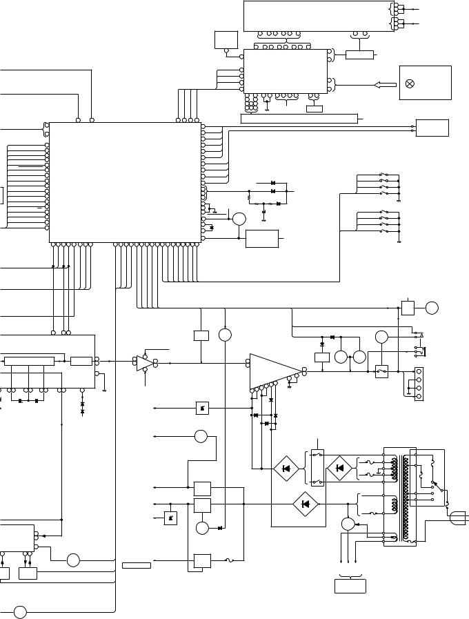
CD-C1W,CP-C1W
|
|
|
|
|
|
|
|
|
|
|
|
|
F2 |
1 |
VF1 (AC) |
|
|
|
|
|
|
|
|
|
|
|
FL 701 |
2 |
|||
|
|
|
|
|
|
|
|
|
|
|
|
3 |
|
||
|
|
|
|
|
|
|
|
|
|
|
FL DIPLAY |
|
62 |
|
|
|
|
|
|
|
|
|
|
|
|
|
|
|
F1 |
63 |
VF2 (AC) |
|
|
|
|
|
|
|
|
|
|
|
|
|
|
64 |
|
|
|
|
|
|
|
RX701 |
|
|
6 ~ 22 |
23 ~ 46 47 ~ 58 |
|
6 ~ 16 |
|
|
|
|
|
|
|
|
|
REMOTE |
|
|
|
|
|
|
|
|
|
|
|
|
|
|
|
CONTROL |
|
|
|
|
|
|
|
|
|
|
|
|
|
|
|
SENSOR |
|
32 |
~ 45 47 ~ 50 52 ~ 71 |
73 ~ 84 |
|
|
|
|
|
|
|
|
|
|
|
1 |
|
|
|
|
|
||||
|
|
|
|
|
|
|
|
|
|
|
30 |
Q702~Q711 +B2 |
|
|
|
|
|
|
|
|
|
|
29 |
|
|
IC701 |
|
~ |
|
|
|
|
|
|
|
|
|
|
|
|
|
39 |
|
|
|
||
|
|
|
|
|
|
|
|
|
|
|
|
|
|
||
TUNER SD |
|
|
|
|
|
DATA1 95 |
|
IX0206AW |
|
|
|
|
|||
|
|
|
|
|
|
COM1 96 |
|
FL DRIVER & |
|
|
|
KEY MATRIX |
|||
|
|
|
|
|
|
|
|
|
|
SW701~SW713 |
|||||
|
|
|
|
|
|
SCK1 |
97 |
|
CONTROLLER |
~ |
|
|
|||
|
|
|
|
|
|
|
|
|
SW717~SW727 |
||||||
|
|
|
|
|
|
|
|
|
|
|
13 |
|
|
|
|
|
|
|
|
|
|
STB 98 |
|
VSS |
VDD |
|
28 |
KEY IN |
|
SW732~SW734 |
|
|
TUNER MUTE |
|
|
|
|
|
|
|
|
|
|
SW739~SW744 |
|||
|
|
|
|
|
|
|
3 |
~ 10 |
15 89 |
18 46 72 90 |
27 28 |
|
|
|
|
|
|
|
|
|
|
|
85 |
~ 87 |
|
|
|
|
|
|
|
|
|
SCK |
COM1 |
DATA1 |
STB |
|
88 91 92 |
|
|
|
|
|
|
|
|
|
|
|
99 |
100 1 |
|
+B2 |
SW702 |
JOG DIAL |
|
|
|
||||
|
|
|
|
|
|
|
|
|
|
|
|
|
|||
|
|
|
8 6 |
7 |
9 |
|
LED701~LED706 |
LED707~LED709 |
LED725,LED726 |
+B6 |
|
|
|||
|
58 |
70 |
|
LED714~LED718 |
LED721~LED724 |
|
|
|
|||||||
|
RES |
|
|
|
|
||||||||||
SPE1~5 |
19 |
|
|
|
91 |
|
|
|
|
|
|
|
|
TO CD UNIT |
|
|
~ |
|
|
|
5 |
CQCK |
|
|
|
|
|
|
|
|
|
–B6 |
23 |
|
|
|
|
|
|
|
|
|
|
|
|
||
|
|
|
|
3 |
COIN |
|
|
|
|
|
|
|
|
|
|
|
|
|
|
|
|
|
|
|
|
|
|
|
|
||
|
TAPE MOTOR |
37 |
|
|
|
|
|
|
|
|
|
|
|
|
|
|
|
|
|
|
|
|
|
|
|
4 |
SQ OUT |
|
|
|
|
|
|
|
|
|
|
|
|
|
|
|
|
|
|
T1 SOLENOID |
39 |
|
|
|
|
|
|
|
|
|
|
|
|
|
|
|
|
|
|
|
|
|
|
|
11 |
WRQ |
|
|
|
|
|
|
|
|
|
|
|
|
|
|
|
|
|
|
T1 CrO |
|
|
|
|
|
|
|
|
|
|
|
|
|
|
|
|
|
|
|
|
|
|
|
|
|
|
|
|
|
|
|
|
|
|
|
|
|
|
|
|
|
||
|
33 |
|
|
|
|
|
|
|
|
|
|
|
|
|
|
|
|
|
|
|
|
|
|
|
94 |
RWC |
|
|
|
|
|
|
|
|
|
|
|
|
|
|
|
|
||
|
T1 RUN |
40 |
|
|
|
|
|
|
|
|
|
|
|
|
|
|
|
|
|
|
|
|
|
|
|
CD SL+ |
|
|
|
|
|
|
|
|
|
|
|
|
|
|
|
|
||
|
T1 PLAY/STOP |
|
|
|
|
|
|
|
|
|
|
|
|
|
|
|
|
|
|
|
|
|
|
|
|
|
|
|
|
|
|
|
|
|
|
|
|
|
|
|
|
|||
|
41 |
|
|
|
|
|
|
|
|
|
|
|
|
|
|
|
|
|
|
|
|
|
|
|
93 |
|
|
|
|
|
|
|
|
|
|
|
|
|
|
|
|
|||
|
HIGH SPEED |
|
|
|
|
|
|
|
|
|
|
|
|
|
|
|
|
|
|
|
|
|
|
|
92 CD-SL– |
|
|
|
|
|
|
|
|
|
|
|
|
|
|
|
|
|||
|
42 |
|
|
|
|
|
|
|
|
|
|
IC201 |
|
|
|
|
|
|
|
|
|
|
|
|
|
|
|
|
|
|
CAM SW1 |
SWB101 |
|
|
|
|||||||||
|
T2 SOLENOID |
38 |
|
|
|
|
|
|
|
|
|
|
|
|
|
|
|
|
|
14 |
CD-PUIN |
|
|
|
|
|
|
|
|
|
|
|
|
|
|
|
||||||||
+B8 |
T2 A FP |
31 |
|
|
|
|
|
|
|
|
|
|
IX0210AW |
|
|
|
|
|
|
13 |
CD-DRF |
|
+B3 |
|
|
|
|
|
|
|
|
CAM SW2 |
SWB102 |
|
|
|
||||||||
|
T2 PLAY/STOP |
|
|
|
|
|
|
|
|
|
|
|
|
|
|
|
|
|
|
|
|
|
|
|
+4.6V |
|
CAM SW3 |
|
|
|
||||||||||||||
|
T2 RUN |
35 |
|
|
|
SYSTEM MICROCOMPUTER |
18 |
+B4 (+4V BACK UP) |
|
|
|
|
|
SWB103 |
|
|
|
|||||||||||||||||||||||||||
|
34 |
|
|
|
|
|
|
|
UNSWITCH |
|
CAM SW4 |
SWB104 |
|
|
|
|||||||||||||||||||||||||||||
|
T2 B FP |
30 |
|
|
|
|
|
|
|
|
|
|
|
|
|
|
|
|
|
|
|
|
|
|
|
VDD 56 |
|
|
|
|
|
|
|
|
|
|
+B2 |
|
|
|
|
|
||
|
|
|
|
|
|
|
|
|
|
|
|
|
|
|
|
|
|
|
|
|
|
|
|
90 |
|
|
|
|
|
|
|
|
|
|
|
|
|
|
|
|
||||
|
T2 CrO |
32 |
|
|
|
|
|
|
|
|
|
|
|
|
|
|
|
|
|
|
|
|
|
|
|
VSS 15 |
|
|
|
|
|
|
|
|
|
|
|
|
|
|
|
|
|
|
|
REC MUTE |
48 |
|
|
|
|
|
|
|
|
|
|
|
|
|
|
|
|
|
|
|
|
|
|
|
+B4 |
|
|
|
|
|
|
|
|
|
|
|
|
|
|
|
|
||
|
|
T1/T2 |
|
|
|
|
|
|
|
|
|
|
|
|
|
|
|
|
|
|
|
|
|
|
|
57 |
|
RESET |
|
|
|
|
|
|
|
|
|
|
TRY SW1 |
SWB105 |
|
|
|
|
|
|
49 |
|
|
|
|
|
|
|
|
|
|
|
|
|
|
|
|
|
|
|
|
|
|
|
89 |
|
|
|
|
|
|
|
|
|
|
|
|
|
|
||||
|
|
|
|
|
|
|
|
|
|
|
|
|
|
|
|
|
|
|
|
|
|
|
|
|
|
|
|
|
|
|
MEMORY |
|
|
|
|
|
|
|
||||||
|
TA-BIAS |
43 |
|
|
|
|
|
|
|
|
|
|
|
|
|
|
|
|
|
|
|
|
|
|
|
12 |
RESET IN |
Q201 |
|
|
|
|
|
BACK UP |
|
|
|
TRY SW2 |
SWB106 |
|
|
|
||
|
REC-EQ |
|
|
|
|
|
|
|
|
|
|
|
|
|
|
|
|
|
|
|
|
|
|
|
|
|
|
|
|
|
|
|
|
|
|
|
||||||||
|
47 |
|
|
|
|
|
|
|
|
|
|
|
|
|
|
|
|
|
|
|
|
|
|
|
16 |
OSC |
|
|
|
|
|
|
|
|
|
|
|
TRY SW3 |
SWB107 |
|
|
|
||
|
PB-EQ |
|
|
|
|
|
|
|
|
|
|
|
|
|
|
|
|
|
|
|
|
|
|
|
|
|
|
|
|
|
|
|
|
|
|
|
|
|
|
|||||
|
46 |
|
|
|
|
|
|
|
|
|
|
|
|
|
|
|
|
|
|
|
|
|
|
|
|
X201 |
|
|
|
|
|
|
|
|
|
|
|
TRY SW4 |
|
|
|
|
||
|
|
|
|
|
|
|
|
|
|
|
|
|
|
|
|
|
|
|
|
|
|
|
|
|
|
|
17 |
4.19MHz |
|
|
|
|
|
|
|
|
|
|
|
SWB108 |
|
|
|
|
|
|
|
|
|
|
|
|
|
|
|
|
|
|
|
|
|
|
|
|
|
|
|
|
|
|
|
|
|
|
Q202 |
|
|
|
|
|
|
|
|
|
|||||
|
|
|
|
|
|
|
|
|
|
|
|
|
|
|
|
|
|
|
|
|
|
|
|
|
|
|
27 |
SYSTEM STOP |
|
|
|
|
+B3 |
|
|
|
|
|
|
|
||||
|
|
|
|
|
|
|
|
|
|
|
|
|
|
|
|
|
|
|
|
|
|
|
|
|
|
|
|
|
Q203 |
|
|
|
|
|
|
|
|
|
||||||
|
|
|
72 |
71 |
69 |
68 |
87 |
53 |
52 |
51 |
|
|
61 |
62 |
63 |
59 |
55 |
28 |
75 |
79 |
54 |
2 |
1 |
100 |
99 98 97 96 95 |
|
|
|
ZD201 |
|
|
|
|
|
|
|
|
|
|
|||||
|
|
|
DO-CCB |
-CCBDI |
CL-CCB |
CE-CCB |
MUTECD |
MUTEPB |
PL/RECDOLBY |
ON/OFFDOLBY |
|
|
SRSA |
SRSB |
INSRSH |
PASSSRS |
FAN |
PROT |
MUTE-S |
POWER |
RELAYSP |
SW4TRY |
SW3TRY SW2TRY |
SW1TRY SW4CAM SW3CAM |
SW2CAM SW1CAM |
|
|
|
P.FAIL DET |
|
|
|
|
|
|
|
|
|
||||||
|
|
|
|
|
|
|
|
|
|
|
|
|
|
|
|
|
|
|
|
|
|
|
|
|
|
|
|
|
|
|
|
|
|
|
|
|
|
|
|
|
+B6 |
M901 |
|
|
|
|
|
|
|
|
|
|
|
|
|
|
|
|
|
|
|
|
|
|
|
|
|
|
|
|
|
|
|
|
|
|
|
|
|
|
|
|
|
|
|
FAN |
|
||
|
|
|
|
|
|
|
|
|
|
|
|
|
|
|
|
|
|
|
|
|
|
|
|
|
|
|
|
|
|
|
|
|
|
|
|
|
|
|
|
|
|
MOTOR |
||
|
|
|
|
|
|
|
|
|
|
|
|
|
|
|
|
|
|
|
|
|
|
|
|
|
|
|
|
|
|
|
|
|
|
|
|
|
|
FAN |
|
|
Q994 |
|
M |
|
|
|
|
|
|
|
|
|
|
|
|
|
|
|
|
|
|
|
|
|
|
|
|
|
|
|
|
S-MUTE |
|
|
|
|
|
|
|
|
|
|
|
|
|
Q995 |
|
|
|
|
|
|
|
|
|
|
|
|
|
|
|
|
|
|
|
|
|
|
|
|
|
|
|
|
|
|
POWER |
|
|
|
|
|
|
|
|
|
|
|
|
|
|
|
||
|
|
|
DI |
|
|
CL |
CE |
|
|
|
|
|
|
|
|
|
|
|
|
|
|
|
|
|
|
|
|
|
|
|
|
|
|
|
|
RELAY |
|
|
|
|
|
|
||
|
|
|
|
|
|
|
|
|
|
|
|
|
|
|
|
|
|
|
|
|
|
|
|
|
|
|
|
|
|
|
|
|
|
|
|
|
|
|
|
|
|
|
|
|
|
|
|
24 |
|
23 |
25 |
|
|
|
|
|
|
|
|
|
|
ICP01 |
|
|
|
|
|
Q905 |
Q828 |
POWER ON/STB |
|
|
|
|
PROT |
|
Q999 |
|
|
|
|||||||||
IC501 |
|
|
|
|
|
|
|
|
|
|
|
|
|
|
|
|
|
|
|
|
|
Q906 |
SWITCHING |
|
|
|
|
|
|
|
|
|
|
|||||||||||
|
|
|
|
|
|
|
|
|
|
|
|
|
|
|
|
|
|
|
|
|
|
|
|
|
|
|
|
|
|
|
|
|
||||||||||||
|
|
|
|
|
|
|
|
|
|
|
|
|
|
|
NJM4565M |
|
|
|
|
|
|
|
|
|
|
|
|
|
|
|
|
|
|
|
|
|
|
|||||||
LC75396N |
|
|
|
|
|
|
|
|
|
|
|
|
|
|
BUFFER AMP. |
|
|
|
|
|
|
|
|
|
|
|
|
|
|
|
|
|
|
|
J901 |
|
||||||||
DIO PROCESSOR |
|
|
|
|
|
|
|
|
|
|
|
|
|
|
|
|
|
|
|
|
+B7 |
|
|
|
|
|
|
|
|
|
|
|
|
|
|
|
|
|
||||||
|
|
|
|
|
|
|
|
OUT |
|
|
|
|
IN |
|
|
|
|
|
|
|
|
|
|
|
|
|
|
|
|
|
|
|
|
|
HEADPHONES |
|||||||||
|
|
|
|
|
|
|
|
|
|
|
|
|
|
|
|
|
8 |
OUT |
|
|
|
|
|
|
|
|
|
|
|
|
|
|
Q903 |
Q997 |
Q998 |
|
|
|||||||
|
|
|
|
|
|
|
|
|
|
|
|
|
L |
|
|
|
L |
5 |
|
|
|
|
|
|
|
|
|
|
|
|
|
|
|
RL901 |
|
|
|
|||||||
GRAPHIC EQUALIZER |
|
|
|
|
VOLUME |
31 |
|
|
|
|
|
7 |
L |
|
|
|
|
|
L-IN |
18 |
IC901 |
|
|
|
Q904 |
|
|
|
||||||||||||||||
|
|
|
|
|
|
|
|
|
|
|
|
|
|
|
|
|
|
|
|
RELAY |
|
|
|
|||||||||||||||||||||
|
|
|
|
17 |
R |
|
|
|
R |
3 |
|
|
|
|
|
|
|
|
|
|
|
|
L-OUT |
|
|
|
|
|
||||||||||||||||
|
|
|
|
|
|
|
|
|
|
|
|
|
|
|
|
|
|
|
|
4 |
|
1 |
R |
|
|
|
|
|
R-IN |
22 |
STK41713 |
|
|
|
|
|
|
|
||||||
|
|
|
|
|
|
|
|
|
|
Vss |
|
|
|
|
|
|
|
|
|
|
|
|
|
|
|
|
|
|
POWER AMP. |
14 |
|
|
+ |
L-CH |
|
|||||||||
|
|
|
|
|
|
|
|
|
|
26 |
|
|
|
|
|
|
|
|
|
|
|
|
|
|
|
|
|
|
15 |
|
|
|
||||||||||||
|
|
|
|
|
|
|
|
|
|
|
|
|
|
|
|
|
|
|
|
|
|
|
|
|
|
|
|
|
|
|
|
|
|
|
|
|
2 |
12 |
|
|
|
|
|
SO901 |
|
|
|
|
|
|
|
|
|
|
|
|
|
|
|
|
|
|
|
|
|
|
|
|
|
|
|
|
|
|
|
|
|
|
VL- VL+ |
R-OUT |
|
|
– |
GND |
|||||
ref |
|
|
|
OUT |
|
|
VDD |
|
|
|
|
|
|
|
|
|
|
|
|
|
|
|
|
|
|
|
|
|
VH+ |
7 |
4 |
|
|
|
|
|
|
|
SPEAKER |
|||||
|
|
|
|
|
|
|
|
|
|
|
|
|
–B6 |
|
|
|
|
|
|
|
|
|
|
VH- |
|
17 |
1 |
|
|
|
|
|
– |
GND |
TERMINALS |
|||||||||
44 4 |
43 5 |
42 6 |
|
48 64 |
|
|
56 |
|
|
|
|
|
|
|
|
|
|
|
|
|
|
|
|
|
|
8 16 |
|
|
|
|
|
|
|
|
||||||||||
|
|
|
|
|
|
|
|
|
|
|
|
|
|
|
|
|
|
|
|
|
|
|
|
|
|
|
|
|
|
|
|
|
||||||||||||
L R |
L R |
L R |
|
L R |
|
|
|
|
|
|
|
|
|
|
|
|
|
|
|
|
|
|
|
|
VOLTAGE |
|
|
|
|
|
|
|
|
|
|
|
|
+ |
R-CH |
|
||||
|
|
|
|
|
|
|
|
|
|
|
|
|
|
|
|
|
|
|
|
|
|
|
|
|
|
|
REGULATER |
|
|
|
|
|
|
|
|
|
|
|
|
|
||||
|
|
|
|
|
|
|
|
|
|
|
|
|
|
|
|
|
|
|
|
|
|
|
|
|
|
|
|
|
|
|
|
|
|
|
|
|
|
|
|
|
|
|
||
|
|
|
|
|
|
|
|
|
|
|
|
|
|
|
|
|
|
|
|
–B6 |
|
|
–15V |
|
|
|
|
|
|
|
|
|
|
|
|
|
|
|
|
|
|
|
||
|
|
|
|
|
|
|
|
|
|
|
|
|
|
|
|
|
|
|
|
|
|
|
|
|
|
|
|
|
|
|
|
|
|
|
|
|
|
|
|
|
|
|
||
|
|
|
|
|
|
|
|
|
+B7 |
|
|
|
|
|
|
|
|
|
|
|
|
|
|
|
|
VOLTAGE |
|
|
|
|
|
|
|
|
|
|
|
|
|
|
|
|
||
|
|
|
|
|
|
|
|
|
|
|
|
|
|
|
|
|
|
|
|
|
|
|
|
|
|
|
|
|
|
|
|
|
|
|
|
|
|
|
|
|
|
|
||
|
|
|
|
|
|
|
|
|
|
|
|
|
|
|
|
|
|
|
|
|
|
|
|
|
|
|
REGULATER |
|
|
|
|
|
|
|
|
|
|
|
|
|
|
|
|
|
|
|
|
|
|
|
|
|
|
|
|
|
|
|
|
|
|
|
|
+B2 |
|
|
+4.6V |
|
Q825 |
|
|
|
|
|
|
|
|
|
|
+B7 |
|
|
T851 |
|
|
|
|||
|
|
|
|
|
|
|
|
|
|
|
|
|
|
|
|
|
|
|
|
|
|
|
|
|
|
|
|
|
|
|
|
|
|
|
|
|
|
|
|
|||||
|
|
|
|
|
|
|
|
|
|
|
|
|
|
|
|
|
|
|
|
|
|
|
|
UN-SWITCHED |
|
|
|
|
|
|
|
|
|
|
RL851 |
|
|
POWER |
|
|
|
|||
|
|
|
|
|
|
|
|
|
|
|
|
|
|
|
|
|
|
|
|
|
|
|
|
|
|
|
|
|
|
–B1 |
|
+B1 |
|
|
|
|
|
|
|
|
|
|||
|
|
|
|
|
|
|
|
|
|
|
|
|
|
|
|
|
|
|
|
|
|
|
|
|
|
|
|
|
|
|
|
|
|
|
RELAY |
|
F857 |
TRANSFORMER |
|
|
|
|||
|
|
|
|
|
|
|
|
|
|
|
|
|
|
|
|
|
|
|
|
|
|
|
|
|
|
|
|
|
|
|
|
|
|
|
|
|
|
|
|
T5A L 250V |
|
230~240V |
T2A L 250V |
|
|
|
|
|
|
|
|
|
|
|
|
|
|
|
|
|
|
|
|
|
|
|
|
+12V(MOTOR) |
VOLTAGE |
|
|
|
|
|
|
|
|
|
|
|
F858 |
|
F856 2.5AT L 250V |
F855 |
|||||
|
|
|
|
|
|
|
|
|
|
|
|
|
|
|
|
|
|
|
|
|
|
|
|
|
|
|
REGULATOR |
|
|
|
|
|
|
|
D851 |
|
|
D850 |
|
|
|
|
SW851 |
|
|
|
|
|
|
|
|
|
|
|
|
|
|
|
|
|
|
|
|
|
|
|
|
|
|
|
|
|
|
|
|
|
|
|
|
|
|
|
|
|
|
|
|
VOLTAGE |
|
|
|
|
|
|
|
|
|
|
|
|
|
|
|
|
|
|
|
|
+B6 |
|
|
|
|
|
Q824 |
|
|
|
|
|
|
|
|
|
|
|
|
T5A L 250V |
|
|
|
SELECTOR |
||
|
|
|
|
|
|
|
|
|
|
|
|
|
|
|
|
|
|
|
|
|
|
|
|
|
VOLTAGE |
Q827 |
|
|
|
|
|
|
|
|
|
|
|
|
|
|
|
|
|
|
|
|
|
|
|
|
|
|
|
|
|
|
|
|
|
|
|
|
|
|
|
|
|
|
|
|
|
|
|
|
|
|
|
|
|
|
|
|
|
|
|
|
|
||
|
|
|
|
|
|
|
|
|
|
|
|
|
|
|
|
|
|
|
|
|
|
|
|
REGULATOR |
|
|
|
|
|
|
|
|
|
|
|
|
|
|
|
|
|
|||
|
|
|
|
|
|
|
|
|
|
|
|
|
|
|
|
|
|
|
+B7 |
|
+12V(ANALOG) |
Q822 |
|
|
|
|
|
|
|
|
|
|
|
|
|
|
|
|
F854 |
|||||
|
|
|
|
|
|
|
|
|
|
|
|
|
|
|
|
|
|
|
|
|
|
|
|
|
|
|
|
|
|
|
|
|
|
|
|
F853 |
|
|
|
|||||
|
|
|
|
|
|
|
|
|
|
|
|
|
|
|
|
|
|
|
|
|
|
|
|
|
|
|
Q823 |
|
|
|
|
|
|
|
|
|
|
|
|
|
|
|
T5A L 250V |
|
|
|
|
|
|
|
|
|
|
|
|
|
|
|
|
|
|
|
|
|
|
|
|
|
|
|
|
|
|
|
|
|
|
|
|
|
|
|
|
T2A L 250V |
|
|
|
||
|
|
|
|
|
|
|
|
|
|
|
|
|
|
|
|
|
|
|
|
|
|
|
|
|
|
|
|
|
|
|
|
|
|
|
|
|
|
|
|
|
|
|
|
|
|
|
|
|
+B8 |
|
|
D852~D854 |
|
|
|
|
|
|
|
|
|
|
|
|
|
|
|
|
|
|
|
Q851 |
|
AC POWER |
|
|
|
|
VOLTAGE |
Q826 |
|
VOLTAGE |
|
|
C451 |
|
28 |
R |
REGURATER |
|
|
|
SUPPLY CORD |
|
5250AS |
27 |
L |
|
SWITCHING |
|
REGULATOR |
T.F |
AC 110/127/220 |
|
|
|
|
|||||||
SRS |
|
|
PASS/SRS STEREO/SRS MONO |
|
|
|
|
|
230–240V |
|
26 |
|
VOLTAGE |
|
|
|
50/60HZ |
||
10 |
25 24 |
|
|
|
REGULATOR |
|
|
|
|
|
|
|
|
|
|
|
|
||
|
|
|
SRS PASS/3D |
+7.3V(CD) |
Q820 |
|
|
|
|
|
|
|
Q464 |
+B9 |
|
|
|
|
|
|
|
|
|
TO CD UNIT |
Q821 |
F820 |
VF1 VP |
VF2 |
|
|
|
|
SRS A/SRS B |
|
T500mA L 250V |
|
|||
|
Q465 |
|
|
|
(AC) |
(AC) |
|
||
67 |
|
|
|
|
|
||||
Q466 |
|
|
|
|
|
|
|
|
|
|
|
|
|
|
|
|
|
|
|
|
|
|
SRS IN H |
|
|
|
TO DISPLAY |
|
|
|
|
|
|
|
|
|
|
||
|
|
|
|
|
|
|
UNIT |
|
|
|
Q463 |
|
SRS PASS |
|
|
|
|
|
|
|
|
|
|
|
|
|
|
|
|
Figure 19 BLOCK DIAGRAM (3/3)
– 19 –

CD-C1W,CP-C1W |
|
|
|
|
|
|
|
|
|
|
|
|
|
|
|
|
|
|
|
|
|
|
|
|
|
|
|
|
|
|
|
|
|
|
|
|
|
|
|
|
|
|
|
|
|
|
|
|
|
|
|
|
|
|
|
|
|
|
|
||
|
|
MAIN PWB-B |
|
|
|
|
|
|
|
|
|
|
|
|
|
|
|
|
|
|
|
|
|
|
|
|
|
|
|
|
|
|
|
|
|
|
|
|
|
|
|
|
|
|
|
|
|
|
|
|
|
|
|
|
|
||||||
A |
|
|
|
|
|
|
|
|
|
|
|
|
|
|
|
|
|
|
|
|
|
|
|
|
|
|
|
|
|
|
|
|
|
|
|
|
|
|
|
|
|
|
|
|
TAPE2 PLAY |
TAPE1 PLAY |
|
|
R- |
||||||||||||
|
|
|
|
|
|
|
|
|
|
|
|
|
|
|
|
|
|
|
|
|
|
|
|
|
|
|
|
|
|
|
|
|
|
|
|
|
|
|
|
|
|
|
|
|
R-CH SENS, |
R-CH SENS, |
|
|
|
|
|||||||||||
|
|
|
B |
|
CT09 |
|
RT19 |
|
|
RT23 |
CT17 |
RT14 |
QT03 |
RT27 |
CT19 |
|
|
|
|
|
|
|
|
|
|
|
|
|
|
|
|
|
|
|
|
|
|
|
|
|
D101 |
|
|
|
|
|
|
|
|
VRD02 |
|
|
|
||||||||
|
|
QT01 |
|
|
CT13 RT21 |
|
|
|
|
|
|
|
|
|
|
|
|
|
|
|
|
|
1 2 3 4 5 6 7 8 9 10 11 |
|
|
|
|
|
D102 |
|
|
VRD04 |
|
|
|
|
|
|
|
|
|
|
|
||||||||||||||||||
|
SW202 |
C |
|
|
RT17 CT11 |
|
|
3 |
|
|
|
|
|
|
|
|
|
|
|
|
|
|
|
|
|
|
|
|
|
|
|
|
QD10 |
|
|
|
|
|
|
||||||||||||||||||||||
|
|
|
|
|
|
|
|
|
|
|
|
|
|
|
|
|
|
|
|
|
|
|
|
|
|
|
|
|
|
|
|
|
|
|
|
|
R |
||||||||||||||||||||||||
|
SPAN |
E |
|
|
|
|
2 |
|
|
|
|
|
|
|
|
|
|
|
|
|
|
|
CNP202 |
|
|
|
|
|
|
|
|
|
|
|
|
|
|
|
|
|
|
|
|
|
|
||||||||||||||||
|
SELECTOR |
|
|
|
|
|
|
|
|
|
|
|
|
|
|
|
|
|
|
|
|
|
|
|
|
|
|
|
TAPE2 PLAY |
|
|
|
|
|
|
|
|
|
|
|
|||||||||||||||||||||
|
100/10 |
|
|
RT15 |
|
|
|
|
|
|
|
|
|
|
|
1 |
|
|
|
|
|
|
|
|
|
|
|
|
|
|
|
|
|
|
C251 |
|
|
|
|
R594 |
|
|
|
|
|
|
|
|
|
|
|
|
|
|
|
||||||
|
|
|
CT15 |
|
|
|
|
|
|
|
|
|
|
|
|
|
|
|
|
|
|
|
|
|
|
|
|
|
|
|
|
|
|
|
|
L-CH SENS, |
|
|
1 |
|
3 2 1 |
|
|
1 2 3 |
|||||||||||||||||
|
|
|
|
8 |
5 |
|
|
|
|
|
|
|
|
|
|
|
|
|
|
|
|
|
|
|
|
|
|
|
|
|
|
|
|
|
|
|
|
|
|
|
|||||||||||||||||||||
|
FM/MW |
|
|
|
|
|
|
|
|
|
|
|
|
|
|
|
|
|
|
|
|
|
|
|
|
|
|
B |
|
|
|
|
|
|
|
|
|
|
|
|
|
2 |
|
3 2 1 |
|
|
|
|
|
|
|||||||||||
|
|
|
|
|
|
ICT01 |
|
|
|
|
|
|
|
|
|
|
|
|
|
|
|
|
|
|
|
|
|
|
|
|
|
|
|
|
|
|
|
|
|
|
|
|
|
|
|
3 |
|
|
|
|
|
|
|
||||||||
|
|
|
|
|
|
|
|
|
|
|
|
|
|
|
|
|
|
|
|
|
|
|
|
|
|
|
|
|
|
|
C |
|
|
|
|
|
|
|
TAPE1 PLAY |
|
|
|
|
|
|
CD |
|||||||||||||||
|
50/9 |
|
|
|
|
|
|
|
|
|
|
|
|
|
|
|
|
|
|
|
|
|
|
|
|
14 |
|
|
|
|
|
|
|
|
|
|
|
|
|
|
|
|
|
|
|
QD09 |
|
|
|
||||||||||||
|
|
|
|
|
|
1 |
4 |
|
|
|
|
|
|
|
|
|
|
|
|
|
|
|
|
|
|
|
|
|
|
|
E |
|
|
|
|
|
|
|
|
|
|
|
|
|
|
|
|
|
|
|
|||||||||||
|
|
|
|
|
|
|
|
|
|
CT18 |
|
|
|
|
|
|
|
|
|
|
|
13 12 |
|
|
|
|
|
|
|
|
|
|
|
|
|
L-CH SENS, |
|
|
|
|
|
|
|
|
|
B C E |
|
||||||||||||||
|
|
|
|
|
|
|
|
|
|
|
|
|
|
|
|
|
|
|
|
|
|
|
|
|
|
|
|
|
Q204 |
|
|
|
|
|
|
|
|
|
|
|
|
|
|
|
|
|
|||||||||||||||
|
|
|
|
|
|
|
|
|
|
|
|
|
|
|
|
|
|
|
|
|
|
|
|
|
11 |
|
|
|
|
|
|
|
|
|
|
|
|
|
|
|
RD75 |
|
|
|
|
|
|
|
|
|
|
|
|
|
|
|
|
|
|||
|
|
|
|
|
|
|
|
|
|
|
|
|
|
|
|
|
|
|
|
|
|
|
|
|
9 |
10 |
|
|
|
|
|
|
|
L251 |
|
|
L252 |
|
|
|
|
|
|
|
|
|
|
|
|
|
|
|
VR151 |
||||||||
|
JT02 |
|
|
|
|
|
|
|
|
|
|
|
|
|
|
|
|
|
|
|
|
|
|
|
|
|
|
|
|
|
|
|
|
|
|
|
|
|
|
|
|
|
|
|
|
|
|
|
|
|
|||||||||||
|
RT09 |
RT11RT12 |
CT07 |
RT16 |
RT18 |
CT16 |
RT22 |
|
|
RT24 |
|
|
RT25 |
|
|
|
|
|
|
|
|
7 |
8 |
CFW852 |
|
|
|
|
|
|
|
|
|
R593 C252 |
|
|
|
|
|
|
|
1 |
QD06 |
VRD01 |
VRD03 |
Q121 |
|
|
|
|
|
|
|||||||||
|
|
|
|
|
|
|
|
|
|
|
|
|
|
6 |
|
|
|
|
|
|
|
|
|
|
|
|
|
CD51 |
|
|
|
|
|
|
|
|
|||||||||||||||||||||||||
|
|
|
|
|
|
|
|
|
|
|
|
|
|
5 |
|
|
|
|
|
|
|
|
|
|
|
|
|
|
|
|
|
|
|
|
|
|
|
|
|
|
|
||||||||||||||||||||
B |
L-CH |
CT08 |
CT10 |
CT12 RT20 |
CT14 |
|
RT41 |
|
|
|
|
|
|
|
|
|
|
3 |
4 |
|
|
|
|
|
|
|
|
|
|
|
|
|
|
|
2 |
|
|
|
|
|
|
C181 |
|
|
|
|
|
|
|||||||||||||
|
|
QT02 |
E |
|
|
|
|
|
|
|
|
|
|
|
|
|
|
|
|
|
|
|
|
1 |
2 |
|
|
|
|
|
|
8 |
FW201 |
|
|
1 |
|
|
TP451 |
|
|
|
3 |
|
|
|
|
|
|
|
|
R173 |
|
|
|
|
|||||
|
LINE OUT |
|
C |
|
|
|
|
|
|
|
RT13 |
|
|
|
|
|
|
|
|
|
|
|
|
|
|
|
|
|
|
|
|
|
|
|
|
|
3 2 1 |
|
|
|
|
QD07 |
|
|
|
|
|
|
|
|
R155 |
|
|
|
|||||||
|
|
B |
|
|
|
|
|
|
|
|
|
|
|
|
|
|
|
|
|
|
|
|
|
|
|
|
|
|
|
|
|
|
|
|
|
|
CD01 |
|
|
RD09 |
|
|
|
|
|
|
|
RD71 |
|||||||||||||
|
|
|
|
|
|
|
|
|
|
|
|
|
|
|
|
|
|
|
|
|
|
|
|
|
|
|
|
|
|
|
|
|
|
|
|
|
|
|
|
|
|
|
|
|
|
|
|
|
|
|
|
|
|||||||||
|
R-CH |
|
|
|
|
|
|
|
|
|
|
|
|
|
|
|
|
|
|
|
|
|
|
|
|
|
|
|
|
|
|
|
|
|
|
|
|
|
|
|
RD15 |
|
|
CD07 |
CD05 |
RD01 |
|
|
|
CD12 |
|
|
CD15 |
|
|
|
|
||||
|
|
|
|
|
|
|
|
|
|
|
|
|
|
|
|
|
|
|
|
|
|
|
|
|
|
|
|
|
|
|
|
|
|
|
|
|
CD09 |
|
|
|
|
|
|
|
|
|
|
|
|
||||||||||||
|
|
|
|
|
|
|
|
|
|
|
|
|
|
|
|
|
|
|
|
|
|
|
|
|
|
|
|
|
|
|
|
|
|
|
|
|
|
|
|
|
|
|
|
|
|
|
|
|
|
|
|
|
|
|
|
|
|
|
|||
|
|
|
|
|
|
|
|
|
|
|
|
|
|
|
|
|
|
|
|
|
|
|
|
|
|
|
|
|
|
|
|
|
|
|
|
|
|
|
|
RD03 |
|
|
|
|
|
|
|
|
|
|
|
|
|
|
|
|
CD1 |
||||
|
|
|
|
|
|
|
|
|
|
|
|
|
|
|
|
|
|
|
|
|
|
|
|
|
|
|
|
|
|
|
|
|
|
|
|
|
|
|
|
|
|
|
|
|
|
|
|
|
|
|
|
|
|
|
|
|
|
C |
|||
|
|
RT10 |
|
|
|
|
|
|
|
|
|
|
|
|
|
|
|
|
|
|
|
|
|
|
E C B |
QP04 |
|
|
|
|
R591 |
R592 |
|
RD29 |
|
|
CD21 CD03 LD01 CD04 |
|
16 |
|
|
|
|
|
|
9 |
|
CD02 |
|
|
|
|
|
||||||||
|
|
|
|
|
|
|
|
|
|
|
|
|
|
|
|
|
|
|
|
|
|
|
|
|
|
|
|
|
|
|
|
15 |
|
|
10 |
|
|
RD10 |
|
|
|
|
|||||||||||||||||||
|
|
|
|
|
|
|
|
|
|
|
|
|
|
|
|
|
|
|
|
|
|
|
|
|
|
|
|
|
|
|
|
|
|
|
|
|
CD06 |
|
|
|
|
|
|
|
|
|
|||||||||||||||
|
|
|
|
|
|
|
|
|
|
|
|
|
|
|
|
|
|
|
|
|
|
|
|
|
CP16 |
|
|
|
|
|
|
|
CD10 |
|
|
|
|
|
|
|
|
|
|
|
|
||||||||||||||||
|
|
|
|
|
|
|
|
|
|
|
|
|
|
|
|
|
|
|
|
|
|
|
RP12 |
|
|
|
|
RP14 |
|
|
|
|
|
|
ICD01 |
|
|
|
|
|
|
|
|
||||||||||||||||||
|
|
|
|
|
|
|
|
|
|
|
|
|
|
|
|
|
|
|
|
|
|
|
|
|
|
|
|
|
|
|
|
|
|
|
|
|
|
|
|
|
|
|
|
||||||||||||||||||
|
|
|
|
|
|
|
|
|
|
|
|
|
|
|
|
|
|
|
|
|
|
|
|
|
|
|
|
|
|
|
|
|
|
|
|
|
|
|
|
RD04 |
|
|
|
1 |
|
|
|
5 |
|
|
8 |
|
|
|
|
|
|
|
|
||
|
|
|
|
|
|
|
|
|
|
|
|
|
|
|
|
|
|
|
|
|
|
|
|
|
|
|
|
|
|
|
|
|
|
|
|
|
|
RD30 |
|
|
|
|
|
|
|
|
|
|
|
|
|
|
|
|
|
||||||
|
|
|
|
|
|
|
|
|
|
|
|
|
|
|
|
|
|
|
|
|
|
|
|
|
|
B C E |
|
QP03 |
|
|
|
|
|
|
|
|
|
|
|
|
|
|
|
|
|
|
|
|
|
|
|
|
|
|
|||||||
|
|
|
|
|
|
|
|
|
|
|
|
|
|
|
|
|
|
|
|
|
|
|
|
|
|
|
|
|
|
|
|
|
|
|
|
|
|
|
|
|
|
|
|
|
|
|
|
|
|
|
|
|
|
|
|||||||
|
|
|
|
|
|
|
|
|
|
|
|
|
|
|
|
|
|
|
|
|
|
|
|
|
|
|
RP13 |
|
|
|
|
|
|
|
|
|
|
|
|
|
|
|
RD02 |
|
|
|
CD13 |
|
E C |
||||||||||||
|
|
|
|
|
|
|
|
|
|
|
|
|
|
|
|
|
|
|
|
|
|
|
|
|
|
|
|
|
|
|
|
|
|
|
|
|
|
|
|
|
|
|
|
|
|
|
|
|
|
|
|||||||||||
|
|
|
|
|
|
|
|
|
|
|
|
|
|
|
|
|
|
|
|
|
|
|
|
CP14 |
|
|
RP11 |
|
|
|
|
|
|
|
|
|
|
|
|
LD02 |
|
CD08 |
|
CD11 |
|
|
|
|
|
|
|
|
RD05 |
|
|
||||||
|
|
|
|
|
|
|
|
|
|
|
|
|
|
|
|
|
|
|
|
|
|
|
|
|
|
|
|
|
|
|
|
|
|
|
|
|
|
|
|
|
|
|
|
|
|
|
|
|
|
|
|
|
|
||||||||
|
|
|
|
|
|
|
|
|
|
|
|
|
|
|
|
|
|
|
|
|
|
|
|
CP08 |
RP08 |
RP06 |
CP15 |
|
|
|
|
|
|
|
|
|
CD40 |
RD28 |
|
CD14RD12 |
|
CD20 |
|
|
|
RD08 |
|
QD02 |
|
|
|
||||||||||
C |
|
|
|
|
|
|
|
|
|
|
|
|
|
|
|
|
|
|
|
|
|
|
|
|
|
|
|
|
|
|
|
|
|
|
|
|
CD18 |
|
|
|
E C B |
|
|
||||||||||||||||||
|
|
|
|
|
|
|
|
|
|
|
|
|
|
|
|
|
|
|
|
|
|
|
|
|
|
|
|
|
|
|
|
|
|
|
|
RD32 |
|
|
|
RD06 |
|
|
|
||||||||||||||||||
|
|
|
|
|
|
|
|
|
|
|
|
|
|
|
|
|
|
|
|
|
|
RP10 |
|
E |
|
|
|
|
|
|
|
|
|
|
|
|
|
|
|
|
|
|
|||||||||||||||||||
|
|
|
|
|
|
|
|
|
|
|
|
|
|
|
|
|
|
|
|
|
|
|
|
|
|
|
|
|
|
|
|
|
|
|
|
|
|
|
|
|
|
RD13 |
|||||||||||||||||||
|
|
|
|
|
|
|
|
|
|
|
|
|
|
|
|
|
|
|
|
|
|
|
CP10 |
RP38 |
C |
QP02 |
|
|
|
|
|
|
|
|
|
|
|
|
RD34 |
|
|
RD35 |
|
|
CD41 |
|
|||||||||||||||
|
|
|
|
|
|
|
|
|
|
|
|
|
|
|
|
|
|
|
|
|
|
|
B |
|
|
|
|
|
|
|
|
|
|
|
|
|
|
|
|
|
|
|
|
C |
|||||||||||||||||
|
|
|
|
|
|
|
|
|
|
|
|
|
|
|
|
|
|
|
|
|
|
|
|
|
|
|
|
|
|
|
|
|
|
CD44 |
|
|
|
|
|
|
|
|
|
||||||||||||||||||
|
|
|
|
|
|
|
|
|
|
|
|
|
|
|
|
|
|
|
|
|
|
|
|
|
|
|
|
|
|
|
|
|
|
|
|
|
|
|
|
|
|
|
|
||||||||||||||||||
|
|
|
|
|
|
|
|
|
|
|
|
|
|
|
|
|
|
|
|
|
|
|
|
|
|
|
|
|
|
|
|
|
|
|
|
|
|
|
|
|
|
|
|
|
|
|
|
|
|||||||||||||
|
|
|
|
|
|
|
|
|
|
|
|
|
|
|
|
|
|
|
|
|
|
|
RP09 RP02 |
|
|
|
CP12 |
|
|
|
CP13 |
|
|
|
|
|
|
|
|
|
|
|
|
|
|
RD27 |
|
|
|
|
|
|
|
|
1 |
|
|
||||
|
|
|
|
|
|
|
|
|
|
|
|
|
|
|
|
|
|
|
|
|
|
|
|
|
|
|
|
|
|
|
|
|
|
|
|
|
|
|
|
|
|
|
|
|
|
|
|
|
|
|
|
|
2 |
|
|
|
|||||
|
|
|
|
|
|
|
|
|
|
|
|
|
|
|
|
|
|
|
|
|
|
|
|
|
|
|
RP07 |
|
|
|
|
|
|
|
|
|
|
|
|
|
|
|
|
|
|
|
|
|
|
|
|
|
|
|
|
|
|
||||
|
|
|
|
|
|
|
|
|
|
|
|
|
|
|
|
|
|
|
|
|
|
|
|
|
R948 |
|
|
|
|
|
|
|
|
|
|
|
|
|
|
|
|
|
|
|
|
|
|
|
|
|
|
|
|
|
3 |
|
|
||||
|
|
|
|
|
|
|
|
|
|
|
|
|
|
|
|
|
|
|
|
|
|
|
|
4 |
|
|
|
|
|
|
|
|
|
|
|
|
|
|
|
|
|
|
|
|
CD38 |
|
|
|
|
|
|
4 |
|
|
|
||||||
|
|
|
|
|
|
|
|
|
|
|
|
|
|
|
|
|
|
|
|
|
|
|
|
1 |
|
|
|
|
|
|
|
|
|
|
|
|
|
|
|
|
|
|
|
|
|
CD45 |
|
|
|
|
|
5 |
|
|
|||||||
|
|
|
|
|
|
|
|
|
|
|
|
|
|
|
|
|
|
|
|
|
|
|
|
|
|
|
|
|
|
|
|
|
|
|
|
|
|
|
|
|
|
DD02 |
|
|
|
|
|
|
|
|
6 |
|
|
|
|||||||
|
|
|
|
|
|
|
|
|
|
|
|
|
|
|
|
|
|
|
|
|
|
|
|
|
|
|
R947 |
|
|
|
|
|
|
|
|
|
|
|
|
|
|
|
|
|
|
|
|
|
|
|
7 |
|
C |
||||||||
|
|
|
|
|
|
|
|
|
|
|
|
|
|
|
|
|
|
|
|
|
|
CP18 |
|
ICP01 |
|
|
|
|
|
|
|
|
|
|
|
|
|
|
|
|
|
|
|
|
|
|
|
|
|
|
8 |
|
|
||||||||
|
|
|
|
|
|
|
|
|
|
|
|
|
|
|
|
|
|
|
|
|
|
|
|
|
|
|
|
|
|
|
|
|
|
|
|
|
|
|
|
|
|
|
|
|
|
|
|
|
|
9 |
|
|
|||||||||
|
|
|
|
CP02 |
|
|
|
|
|
|
|
|
|
|
|
|
|
|
|
|
|
5 |
8 |
|
|
|
CP17 |
|
|
|
|
|
|
|
|
|
|
|
|
|
|
|
|
|
|
CD42 10 |
|
|
|
||||||||||||
|
|
|
|
|
|
|
|
|
|
|
|
|
|
|
|
|
|
|
|
|
|
|
|
|
|
|
|
|
|
|
|
|
|
|
|
|
|
|
|
|
|
|
11 |
|
|||||||||||||||||
|
|
|
|
|
|
|
|
|
|
|
|
|
|
|
|
|
|
|
|
|
|
|
|
|
|
|
|
|
|
|
|
|
|
|
|
|
|
|
|
|
RD37 |
|
|
CD34 |
|||||||||||||||||
|
|
|
|
|
|
|
|
|
|
|
|
|
|
|
|
|
|
|
|
|
|
|
|
|
|
|
|
|
|
|
|
|
|
|
|
|
|
|
|
|
|
|
|
|
|
|
|
|
|
|
12 |
|
|||||||||
|
|
|
|
|
|
|
|
|
|
|
|
|
CP01 |
|
|
R942 |
|
|
|
|
|
|
|
|
|
|
|
|
|
|
|
|
|
|
|
|
|
|
|
|
|
|
|
|
|
|
ICD03 |
|
|||||||||||||
|
|
|
|
|
|
|
|
|
|
|
|
|
|
|
|
|
|
|
|
|
|
|
RP37 |
|
|
|
|
|
|
|
|
|
|
|
|
|
|
|
|
|
|
|
|
|
|
|
|
|
|
|
|||||||||||
|
|
|
|
|
|
|
|
|
|
|
|
|
|
|
R941 |
|
|
|
CP07 RP05 CP11 |
|
|
|
|
|
|
|
|
|
|
|
|
|
|
|
|
|
|
|
|
|
|
|
|
|
|
|
|
|
|||||||||||||
|
|
|
|
|
|
|
|
|
|
|
|
|
|
|
|
|
|
|
|
|
|
|
CP09 |
|
|
|
|
|
|
|
|
|
|
|
|
|
|
|
|
|
|
|
|
|
|
|
|
|
|
|
|
|
|
|
|
|
|
|
|||
D |
|
|
|
|
|
|
|
|
|
|
|
|
|
|
RP16 |
|
|
RP01 |
|
E C B |
|
|
|
|
|
|
|
|
|
|
|
|
|
|
|
|
|
|
|
|
|
|
|
|
|
|
|
|
|
|
|
|
|
|
|
||||||
|
|
|
|
|
|
|
|
|
|
|
|
|
|
RP15 |
|
|
QP01 |
|
|
|
|
|
|
|
|
|
|
|
|
|
|
|
|
|
|
|
|
|
|
|
|
|
|
|
|
|
|
|
|
|
|
|
|||||||||
|
|
|
|
|
|
|
|
|
|
|
|
|
|
|
|
|
|
|
|
|
|
|
|
|
|
|
|
|
|
|
|
|
|
|
|
RD21 |
|
|
|
|
|
|
|
|
|
|
|
|
|
|
|
|
|
||||||||
|
|
|
|
|
|
|
|
|
|
|
|
|
|
|
|
|
|
|
|
|
|
|
|
|
|
|
|
|
|
|
|
|
|
|
|
|
|
|
|
|
|
|
|
|
|
|
|
|
|
|
|
|
|
|
|
|
|
|
|||
|
|
|
|
|
|
|
|
|
|
|
|
|
|
|
|
|
|
|
|
|
|
|
|
|
|
|
|
|
|
|
|
|
|
|
|
|
|
|
|
|
|
RD22 |
|
|
|
|
|
|
|
|
|
|
|
|
|
|
|
|
|
|
|
|
|
|
|
|
R516 |
|
|
|
|
C549 |
|
|
|
1 |
|
|
|
|
|
|
|
|
|
|
|
|
|
|
|
|
|
|
|
|
|
|
|
|
|
|
|
|
|
|
|
|
|
|
|
|
|
|
|
|
|
|
|
|
|
||
|
|
|
|
|
|
|
R514 |
|
|
|
|
2 |
QT04 |
|
|
|
|
|
|
|
|
|
|
|
|
|
|
|
|
|
|
|
|
|
|
|
|
|
|
|
|
|
|
|
|
|
|
|
|
|
|
|
|
|
|
|
|
||||
|
|
|
|
|
|
|
|
C554 |
|
|
|
|
3 |
|
|
C556 |
|
R502 C532 |
|
C530 |
|
C528 |
|
|
|
|
|
|
|
|
|
|
|
|
|
|
|
R491 |
|
|
|
|
|
|
R481 |
C461 |
R480 |
|
R484 |
R479 |
C460 |
|
|
|
|
||||||
|
|
|
|
|
R515 |
|
|
|
|
|
|
|
|
C541 |
|
|
|
|
C526 |
|
|
|
|
|
|
Q458 |
1 2 3 |
C472 |
R490 |
R492 |
|
|
|
|
|
|
|
||||||||||||||||||||||||
|
|
|
|
|
|
|
|
|
|
|
|
|
|
|
|
C522 |
|
|
|
|
|
|
|
|
|
S |
|
|
|
|
|
|
|
||||||||||||||||||||||||||||
E |
|
|
|
|
C553 |
|
|
|
C551 |
|
|
|
|
|
|
|
|
|
C540 |
|
|
|
|
|
R518 |
|
|
|
|
|
D403 |
|
|
G |
|
|
|
R482 |
|
|
|
|
|
|
|
Q460 |
|
||||||||||||||
|
|
|
|
|
|
|
|
|
|
|
|
|
|
|
|
|
|
|
|
|
|
|
|
|
|
|
|
C548 |
|
|
|
|
|
|
|
|
|
|
|
|
|
|
R483 |
|
|
|
|
|
|
||||||||||||
|
|
|
R513 |
|
|
|
|
|
|
|
R509 |
R511 |
R510 |
|
|
|
|
|
C524 |
|
|
|
|
|
|
|
|
|
|
R470 |
|
D |
|
|
|
|
|
|
|
|
|
|
|
|
|
Q46 |
|||||||||||||||
|
|
|
|
|
|
|
|
C543 |
|
|
|
|
|
|
|
|
|
|
|
|
|
|
|
|
|
|
|
|
|
|
|
|
|
|
|
|
|
|
1 |
|
|
|
|
|
|||||||||||||||||
|
|
|
|
|
|
|
|
|
|
|
|
|
|
|
C534 |
|
|
|
|
|
|
|
C557 |
|
|
|
|
|
|
|
|
14 |
|
10 |
|
|
|
5 |
|
|
|
|
|
|
|
|
|
||||||||||||||
|
|
|
|
|
C581 |
R512 |
|
|
|
C552 |
|
|
17 |
16 |
|
|
C518 |
|
|
|
|
|
|
|
C547 |
Q467 |
|
|
|
|
|
|
|
C458 |
|
|
|
|
|
|
|||||||||||||||||||||
|
|
|
|
|
|
|
|
|
|
|
|
|
|
|
|
|
|
|
|
|
|
|
|
|
|
|
|
|
|
|
|
|
|
|
|||||||||||||||||||||||||||
|
|
|
|
|
|
|
|
|
|
|
|
|
|
|
|
C558 |
|
|
|
|
|
|
|
|
|
IC451 |
|
|
|
|
|
|
|
|
|
|
|
||||||||||||||||||||||||
|
|
|
|
|
|
|
|
|
|
|
|
|
|
|
|
|
|
|
|
|
|
|
R517 |
|
|
|
|
|
|
|
|
|
|
|
|
R466 |
|
|
|
|
|
||||||||||||||||||||
|
|
|
|
|
|
|
C550 |
|
|
2015 |
|
|
|
|
C516 |
|
|
|
|
|
|
|
|
15 |
20 |
|
|
|
25 |
|
28 |
|
R493 |
|
|
||||||||||||||||||||||||||
|
|
|
|
|
|
|
|
|
|
|
|
|
|
|
|
|
|
|
|
|
|
|
|
|
|
|
|
|
|||||||||||||||||||||||||||||||||
|
|
|
|
|
|
|
|
|
|
|
25 |
10 |
|
|
|
|
|
|
|
|
|
|
|
|
|
|
|
|
|
|
|
|
|
|
|
|
|
|
R |
||||||||||||||||||||||
|
|
|
|
|
|
|
|
|
|
|
C582 |
|
|
|
|
|
|
|
|
|
|
|
|
|
|
|
|
|
|
|
|
|
|
|
|
|
|
|
|
|
|
||||||||||||||||||||
|
|
|
|
|
C555 |
|
R501 |
|
|
C542 |
|
|
|
|
30 |
|
|
|
5 |
|
|
|
|
C546 |
|
|
C510 |
|
|
|
|
|
|
|
R471 |
|
|
R465 |
|
|
|
|
|
|
|
|
|
|
|
|
|
|
|
||||||||
|
|
|
|
|
|
|
|
|
|
|
32 |
|
|
|
|
1 |
|
C512 |
|
|
|
|
|
|
|
|
|
|
|
|
|
|
|
|
|
|
|
|
|
|
|
|
|
|
|
||||||||||||||||
|
JT01 |
|
|
|
|
|
|
|
|
|
|
|
|
|
|
|
|
|
|
R522 |
|
|
|
|
|
|
|
|
|
|
|
|
|
|
|
|
|
|
|
|
|
|
|
|
|
||||||||||||||||
|
|
|
|
|
|
|
|
|
|
|
|
|
|
33 |
35 |
IC501 |
|
60 |
|
64 |
R504 |
|
|
|
|
|
|
|
|
|
|
|
|
|
|
|
|
|
|
|
|
|
|
|
|
R488 |
|
|
|
|
|
|
|
1 |
|||||||
|
VIDEO/AUX |
|
|
|
|
|
|
|
|
|
|
|
|
|
|
|
|
|
|
|
|
C536 |
|
|
|
|
|
|
|
|
|
|
|
|
|
R487 |
|
|
|
|
|
|
|
|
|
||||||||||||||||
|
|
|
|
|
|
|
|
|
|
|
|
|
|
|
|
|
40 |
55 |
|
|
|
|
R506 |
|
|
|
|
|
|
|
|
|
|
|
|
|
|
|
|
|
|
|
|
|
|
|
|
|
|
|
|||||||||||
|
|
|
|
|
|
C539 |
|
|
|
|
|
|
|
|
|
|
|
|
|
|
|
|
|
|
R477 |
|
|
|
|
|
|
|
R469 |
|
|
|
|
|
|
|
|
|
|
|
|
|
|
|
|
E |
|||||||||||
|
L-CH |
|
|
|
|
|
|
|
C533 |
|
|
|
|
|
|
4550 |
|
|
|
|
C508 |
|
|
|
|
|
|
|
|
C481 |
|
C483 |
|
C453 |
|
|
|
|
R468 |
|
|
|
|
|
|
|
|
|
|||||||||||||
|
|
|
|
|
|
|
|
|
|
|
|
|
|
|
|
|
|
|
|
C579 |
|
|
|
|
|
|
|
|
R455 |
R459 |
C471 |
|
|
|
|
|
C457 |
|
|
|
|||||||||||||||||||||
|
|
|
|
|
|
|
|
C531 |
|
|
|
|
|
|
|
|
|
|
|
|
|
C504 |
|
|
|
|
|
|
|
|
|
|
|
|
|
C454 |
|
|
|
|
|
|
|||||||||||||||||||
|
|
|
|
|
|
|
|
|
C529 |
|
|
|
|
|
|
|
48 |
49 |
|
|
|
|
|
|
|
|
|
C506 |
|
|
|
|
|
|
|
|
|
|
|
|
|
|
|
|
|
||||||||||||||||
|
|
|
|
RT05 |
|
|
|
|
|
|
|
|
C517C521 |
|
|
|
|
C578 |
|
|
|
C502 |
|
C487 |
|
8 |
9 |
10 11 12 13 14 |
|
|
|
|
|
|
|
|
|
R467 |
|
|
|
C |
|||||||||||||||||||
|
VIDEO-OUT |
|
|
|
|
|
C527 |
|
|
C525 |
C523 |
|
|
C515 |
|
C511 |
|
|
D502 |
|
|
|
ZD451 |
|
|
|
|
|
|
|
|
|
|
|
|||||||||||||||||||||||||||
|
|
|
|
|
|
|
|
|
|
|
|
|
|
|
|
|
|
|
|
|
|
|
|
|
|
IC452 |
|
|
|
|
|
C485 |
|
|
|
|
|
|
|
|
|
|
|||||||||||||||||||
|
|
|
|
|
|
|
|
|
|
|
|
|
|
R503 |
|
|
|
|
|
|
|
|
|
|
|
|
|
|
|
|
|
|
|
|
|
|
|
Q201 |
|||||||||||||||||||||||
F |
|
|
|
|
|
|
|
|
|
|
|
|
|
|
|
|
|
|
|
|
|
|
|
|
6 |
5 |
|
|
|
|
R462 |
|
|
|
|
|
|
|
|
||||||||||||||||||||||
R-CH |
|
|
RT06 |
|
|
|
|
|
|
|
|
|
|
|
|
C501 |
|
|
|
|
|
|
|
7 |
4 |
3 |
2 |
1 |
|
|
|
|
D205 |
|
|
|
|
1 |
|||||||||||||||||||||||
|
|
|
|
|
|
|
|
|
|
|
|
|
|
|
|
|
|
|
|
|
|
|
|
|
|
|
|
|
|
|
|
|
|
|
|
||||||||||||||||||||||||||
|
|
|
|
|
|
|
|
|
|
|
|
|
|
|
|
|
|
C503 |
|
|
|
|
|
|
|
|
|
|
|
|
|
|
|
|
|
|
|
|
|
|
2 |
||||||||||||||||||||
|
|
|
|
|
|
|
|
|
|
|
CT03 |
|
|
|
|
|
C545 |
|
R505 |
C507 |
|
|
|
|
|
|
|
|
|
R521 |
C488 |
ZD452 |
C482 |
R456 |
|
R460 |
|
R472 |
R461 |
|
1 |
C486 |
3 |
|
Q451 |
R236 |
C204 |
|
|
|
3 |
||||||||||
|
|
|
DT02 |
DT01 |
|
|
CT04 |
RT08 |
|
|
RT07 |
C509 |
|
|
|
C505 |
D501 |
|
|
|
|
|
C484 |
|
|
2 |
2 |
|
R237 |
||||||||||||||||||||||||||||||||
|
|
CT05 |
|
|
|
|
|
C535 |
|
|
|
|
|
|
|
|
|
3 |
1 |
|
|
|
|
|
R230 |
||||||||||||||||||||||||||||||||||||
|
|
|
|
|
|
|
|
|
|
|
|
|
|
|
|
|
|
|
|
|
|
|
|
|
|||||||||||||||||||||||||||||||||||||
|
|
|
|
|
|
|
|
|
|
|
|
|
|
|
|
|
|
|
Q452 |
|
|
|
|
|
|
||||||||||||||||||||||||||||||||||||
|
|
|
|
|
|
|
|
|
|
|
Q828 |
D827 |
|
|
|
|
|
|
|
|
|
|
|
|
|
|
|
|
|
|
|
|
|
|
|
|
|
|
|
|
Q501 |
|
|
|
|
|
|
|
|
|
|
|
D202 |
|
|
|
|
||||
|
|
|
|
|
|
|
|
|
|
|
|
|
|
D829 |
R835 |
|
D826 |
|
ZD820 |
|
|
|
|
|
|
|
|
|
|
|
|
|
|
|
|
|
|
|
C E B R595 |
|
|
|
|
|
C207 |
|
|
|
|
||||||||||||
|
|
|
|
|
C827 |
C833 |
|
|
|
3 |
|
Q826 |
|
|
|
|
|
|
|
|
|
|
|
|
|
|
|
|
|
|
|
|
|
|
|
|
|
|
|
|
|
|
|
|
|
||||||||||||||||
|
|
|
|
|
|
|
|
|
|
|
C824 |
C823 |
|
|
|
|
|
|
|
|
|
|
|
|
|
|
|
|
|
|
|
|
|
|
|
|
|
|
|
|
|
|
|
|
|
|
|
|
|
|
|||||||||||
|
|
Q825 |
|
C826 |
|
|
|
2 |
|
|
3 |
C825 |
|
|
|
|
|
|
|
|
|
|
|
|
|
|
|
C E B |
|
|
|
|
|
|
|
|
|
|
|
|
|
|
|
|
|||||||||||||||||
|
|
|
|
|
|
|
|
|
1 |
|
|
2 |
|
|
|
|
|
|
|
|
|
|
|
|
|
|
|
R596 |
|
|
|
|
|
|
|
|
|
|
|
|
|
|
|||||||||||||||||||
|
|
|
|
B C E |
|
|
|
|
|
|
|
|
|
|
|
|
|
|
|
|
|
F820 |
|
|
|
|
|
|
|
|
Q502 |
|
|
|
|
|
|
|
|
|
|
|
|
|
|
|
|||||||||||||||
|
|
|
|
|
|
|
|
|
|
|
|
|
|
|
|
|
|
|
|
|
|
|
|
|
|
|
|
|
|
|
|
|
|
|
|
|
|
|
|
|
|
|
|
|
|
|
|
|
|
|
|
|
|||||||||
|
|
|
|
|
|
|
|
|
|
R834 |
|
1 |
R825 |
|
|
|
|
|
|
|
|
|
|
|
|
|
|
|
|
|
|
|
|
|
|
|
|
|
|
|
|
|
|
|
|
|
R210 |
|
|
|
|
|
|||||||||
|
|
|
|
|
|
|
|
|
|
|
|
|
|
|
|
|
|
|
|
|
|
ZD822 |
|
C820 |
C821 |
T500mA L 250V |
|
|
|
|
|
|
|
|
|
|
|
|
|
|
|
|
|
|
|
|
|
|
|
||||||||||||
|
|
|
R827 |
|
|
|
|
|
|
|
|
|
|
|
|
|
|
|
|
|
|
|
|
|
|
|
|
|
|
|
|
|
|
|
|
|
|
|
|
|
|
|
|
|
|
|
|
|
|||||||||||||
|
|
|
|
|
R829 |
R823 |
|
|
|
|
|
|
|
|
R824 |
|
|
R820 |
|
Q821 |
D823 |
|
|
|
|
|
|
|
|
|
|
|
|
|
|
|
|
|
|
|
|
|
|
|
|
|
|
|
|
|
|
||||||||||
G |
|
|
|
|
|
|
|
|
|
|
|
|
|
|
|
|
|
|
R822 |
|
|
|
|
|
|
|
|
|
|
|
|
|
|
|
|
|
|
|
|
|
|
|
|
|
|
|
|
|
|
|
|||||||||||
|
|
ZD821 |
|
Q827 |
B C E |
|
|
C822 |
B C E |
|
|
|
E C B |
|
|
|
|
|
|
|
|
|
|
|
|
|
|
|
|
|
|
|
|
|
|
|
|
|
|
|
|
|
|
||||||||||||||||||
|
|
R828 |
|
|
|
|
|
|
|
|
|
|
Q823 |
|
|
|
|
|
|
|
|
C830 |
|
|
|
|
|
|
|
|
|
|
|
|
|
|
|
|
|
|
|
|
|
|
|
||||||||||||||||
|
|
|
|
|
|
E C B |
|
|
B C E |
|
|
B C E |
|
D821 |
|
|
|
|
|
|
|
|
|
|
|
|
|
|
|
|
|
|
|
|
|
|
|
|
|
|
|||||||||||||||||||||
|
|
|
Q824 |
|
|
|
|
|
|
|
|
|
|
|
|
|
|
|
|
|
|
|
|
|
|
|
|
|
|
|
|
|
|
|
|
|
|
||||||||||||||||||||||||
|
|
|
|
|
|
|
|
|
|
|
|
|
|
Q822 |
|
|
|
|
|
|
|
|
|
|
Q820 |
|
|
|
|
|
|
|
|
|
|
|
|
|
|
|
|
|
|
|
|
|
|
|
|
|
|
|
|
|
|
|
|||||
|
|
|
|
|
|
|
|
|
|
|
|
|
|
|
|
|
|
|
|
|
R826 |
|
|
|
|
|
|
|
|
|
|
|
D822 |
|
|
|
|
|
|
|
|
CNP851 |
|
|
|
|
|
|
26 24 22 20 18 16 1 |
||||||||||||
|
|
|
|
|
|
|
|
|
|
|
|
|
|
|
|
|
|
|
|
|
|
|
|
|
|
|
|
|
|
|
|
|
|
|
|
|
|
|
|
|
|
|
|
|
|
|
|
|
|
|
|||||||||||
|
|
|
|
|
|
|
|
|
C831 |
|
|
|
|
|
|
|
|
|
|
|
|
|
|
|
|
|
|
|
|
|
|
|
|
|
|
|
|
|
1 |
2 |
3 |
|
4 |
|
|
|
|
|
27 25 23 21 19 17 15 |
||||||||||||
|
|
|
|
|
|
|
|
|
|
|
|
|
|
|
|
|
|
|
|
|
|
|
|
|
|
|
|
|
|
|
|
|
|
|
|
|
|
|
|
|
|
|
|
|
|
|
|
|
|
|
|
|
|
|
|
|
|
|
|
|
|
H |
|
|
|
|
|
|
|
|
|
|
|
|
|
|
|
|
|
|
|
|
|
|
|
|
|
|
|
|
|
|
|
|
|
|
|
|
|
|
|
|
|
|
|
|
|
|
|
|
|
|
|
|
|
|
|
|
|
|
|
|
|
|
1 |
|
|
2 |
|
|
|
|
|
|
|
|
|
|
|
|
3 |
|
|
|
|
|
|
|
|
|
|
|
|
4 |
|
|
5 |
|
|
|
|
|
|
|
|
|
|
|
|
|
|
6 |
|
|
|
|
|
|
|
|
|
||||
Figure 20 WIRING OF P.W.BOARD (1/7)
– 20 –
CD-C1W,CP-C1W
LAY |
TAPE1 PLAY |
|
|
R-CH REC/PLAYSENS, |
|
|
|
|
|
|
|
|
|
|
|
|
|
|
|
|
|
L-CH BIAS |
|
|
|
|
|
|
|
|
|
|
|
|
L-CH BIAS |
|
|
|
|
|
|
|
|
|
|
|
|
|
|
1 |
|
14 |
|||||||||||||||||||||||||
NS, |
R-CH SENS, |
|
|
|
|
|
|
|
|
|
|
|
|
|
|
|
|
|
|
|
|
|
|
|
|
|
|
|
|
|
|
|
|
CURRENT |
R105 |
E R103 |
|
|
|
|
|
|
|
|
|
|
|
|
|
R167 Q128 |
|
|
|
|
|
C162 L104 |
|
|
|
|
|
|
|||||||||||||||
1 |
3 2 1 |
|
|
|
1 2 3 |
|
QD08 |
|
|
|
|
CD16 |
|
|
|
|
|
C178 |
C180 |
R196 |
Q150 |
|
R194 |
R180R126 |
C168 |
3 |
|
|
C118 |
C124 |
|
|
|
|
|
E |
R104 |
|
E |
R111R106 |
RP101 |
|
C151 |
R168 |
|
|
|
|
CFW903 |
P38 6-C |
|||||||||||||||||||||||||||
|
|
|
Q121 |
|
|
|
|
|
|
|
|
|
|
|
|
|
|
|
|
|
|
|
|
|
|
|
|
|
|
|
|
|
|
|
|
|
|
|
|
|
|
|
|
|
CURRENT |
|
Q124 |
|
|
|
|
|
|
|
|
|
|
|
|||||||||||||||||||
|
|
|
|
VRD02 |
|
|
|
|
VR152 |
|
|
|
R154 |
Q122 |
|
|
|
|
|
Q154 |
|
|
C170 |
Q148 |
Q114 |
|
|
Q105 |
|
|
|
|
|
|
|
|
|
|
|
|
|
|
|
|
|
|
|
|
|
|
|
|
|
C150 |
|
|
|
FW903 |
|||||||||||||||||||
3 |
|
|
|
|
|
|
|
CD52 |
|
|
|
|
|
|
|
|
|
|
|
|
|
|
|
|
|
|
|
|
|
Q140 |
VR101 |
|
|
|
4 3 2 1 |
|
|
|
|
|
|
|
|
R141 |
|
|
|
|
|
|
|
|
|
R166 |
|
|
|
|
|
||||||||||||||||||
VRD04 |
|
|
QD10 |
|
|
|
|
|
|
|
|
|
|
|
|
|
|
|
|
|
B |
|
|
|
|
|
|
3 2 1 |
|
1 2 3 |
1 |
|
1 2 3 |
|
|
|
B |
|
C |
|
|
C |
|
Q106 |
|
|
C152 |
|
|
|
|
C |
|
|
|
|
|
|
|
|
|
|
|
||||||||||||||
|
|
|
|
|
|
|
|
|
|
|
|
|
|
|
|
|
|
|
|
|
|
|
|
|
|
|
|
|
|
|
|
|
|
|
|
|
|
|
|
E |
|
|
|
|
|
C |
|
|
|
|
|
|
|
|
|
|
|
|
|
|
|
|
|
|
|
|
|||||||||||
|
|
|
|
|
|
|
|
|
|
R174 |
|
|
|
|
|
|
|
|
C |
|
|
|
|
|
|
|
|
|
|
|
|
|
|
|
|
|
|
|
|
|
|
C |
|
B |
|
|
B |
|
|
B |
|
|
|
|
|
|
|
|
|
|
|
|
|
|
|
|
|
|
|
|
|
|
|||||
|
|
|
|
C181 |
|
|
|
|
|
|
|
|
R156 |
|
|
|
|
|
E |
2 1 0 L |
R198 |
|
|
|
C134 |
3 2 1 |
C126 |
R132 |
|
R124 |
2 |
|
|
|
|
|
|
|
|
|
|
|
|
|
|
|
|
|
|
|
|
|
|
|
|
|
|
|
B |
|
|
|
|
|
|
|
|
Q127 |
|
|
|
||||||
|
|
|
|
|
|
|
|
|
|
|
|
|
|
|
|
|
|
|
|
|
C176 |
RD78 R138 |
|
|
|
|
|
|
|
|
|
|
|
|
|
|
|
|
|
|
|
|
|
|
|
|
|
|
|
|
|
|
|
|
|
|
|
|
|
|
|
||||||||||||||||
2 |
3 2 1 |
|
|
|
|
|
|
|
|
|
|
C182 |
|
|
|
|
|
|
|
|
|
|
|
|
|
|
|
|
|
|
|
R128 |
|
|
|
|
|
TP490 |
|
|
|
|
|
|
VR102 |
|
|
|
|
|
|
|
R160 |
|
|
|
|
|
|
|
|
TO POWER AMP. PWB |
|||||||||||||||
|
|
|
|
|
|
|
|
|
|
|
|
|
R149 |
|
|
C145 |
|
R157 |
R150R152 |
C142 |
C147R192 |
|
C140 |
136R |
C130 |
C132 |
R130 |
|
|
|
C112 |
R120 |
|
|
|
C108 |
|
|
|
|
|
|
|
|
|
|
R161 |
R186 |
R164 |
|
|
|
|
|
|
FROM TAPE 2 HEAD PWB |
|||||||||||||||||||||
|
|
VRD03 |
|
|
|
|
|
|
|
|
|
|
|
|
|
|
|
|
|
|
|
|
|
C114 C120 |
R122 |
|
|
|
|
|
|
|
Q108 |
R115 |
|
|
|
|
|
|
R185 |
|
|
|
|
|
|
||||||||||||||||||||||||||||||
|
|
QD09 |
|
|
|
|
|
|
RD72 |
|
|
|
|
|
|
|
|
|
|
|
|
|
|
|
|
|
|
|
|
|
|
|
|
|
|
|
|
|
|
|
|
|
|
|
|
|
|
|
|
|
|
|
|
|
|
|
|
|
E C B |
|
|
|
|
|
|
|
|
|
|
||||||||
|
|
|
|
|
|
B C E |
|
|
R153 |
|
|
Q119 |
|
|
|
|
|
|
|
|
|
|
|
|
|
|
|
|
|
|
|
|
|
C105 |
|
|
R112 C106 |
|
|
|
|
|
|
|
R113 |
R162 |
|
|
|
|
|
|
R163 |
|
|
CNP303 |
|
||||||||||||||||||||
|
|
|
|
|
|
|
VR151 |
|
|
|
|
3 2 1 |
|
|
|
|
|
|
|
|
|
|
|
|
|
|
|
|
|
|
C116 |
|
|
|
R189 |
|
|
|
R190 |
|
|
|
|
C109 |
|
|
|
|
|
|
|
|
|
|
|
E C B |
3 |
|
|
|
|
||||||||||||||||
RD01 |
|
|
|
|
|
|
|
|
|
|
|
L-CH |
|
|
|
|
|
|
|
|
|
|
|
|
|
|
|
|
|
|
|
|
|
|
|
|
|
|
|
|
|
|
7 6 5 4 3 2 1 |
CNP102 |
|
|
|
|
|
|
|
|
|
|
|
|
Q125 |
|
2 |
|
TO TUNER PWB |
||||||||||||||||
|
|
|
|
|
|
|
|
|
|
|
|
|
|
|
|
|
|
|
|
|
|
|
|
|
|
|
|
|
|
|
|
|
|
|
|
|
|
|
|
|
|
|
|
|
|
|
|
|
|
|
|
|
|
|
|
|
|
|
|
R165 |
1 |
|
|
P29 11-A |
|
||||||||||||
|
|
|
|
|
|
|
|
|
|
|
|
|
REC/PLAY |
|
|
|
|
|
|
|
|
|
|
|
|
|
|
|
|
|
|
|
|
|
|
|
|
R118 |
|
|
|
|
|
|
|
|
|
|
|
|
Q109 |
B C E |
|
|
|
|
|
|
|
|
|
|
3 2 1 |
|
|
|
|||||||||||
|
|
|
|
|
|
|
|
|
|
|
|
|
SENS, |
|
|
|
|
|
|
|
|
|
|
|
|
|
|
|
|
|
|
|
C122 |
|
|
|
|
|
|
|
|
R140 R108 |
|
|
C148 |
|
|
|
|
|
|
Q126 |
|
|
|
||||||||||||||||||||||
|
|
|
|
|
R173 |
|
|
|
|
|
|
|
|
|
|
|
|
|
|
|
|
|
|
|
|
|
|
|
|
|
|
|
|
|
|
|
R139 |
|
|
|
|
|
|
|
|
|
|
|
|
|
|
|
|
|
|
|
|
||||||||||||||||||||
|
|
|
|
|
|
|
|
|
|
|
|
|
|
|
|
|
|
|
|
|
|
|
|
|
|
|
|
|
|
|
|
|
|
|
|
|
|
|
|
|
|
|
|
|
|
|
|
|
|
|
|
|
|
|
|
|
|
|
|
|
|
|
|
||||||||||||||
|
|
|
|
|
|
|
|
|
|
|
|
|
|
|
|
|
|
|
|
|
|
|
|
|
|
|
|
|
|
|
|
|
|
|
|
|
|
|
|
|
|
|
|
|
|
|
|
|
|
|
|
|
|
|
|
|
|
|
|
|
|
|
|
|
|
|
|
|
|
|
|
|
|
||||
|
|
|
|
|
|
R155 |
|
|
|
|
R158 |
|
|
|
|
|
|
|
|
|
|
13 |
|
15 |
|
|
|
20 |
|
|
24 |
|
|
|
R117 |
E |
|
|
|
|
E C B |
|
|
|
|
|
|
|
|
|
|
D555 R571 D554 |
|
|
|
|
|
|
|
|
|
|
|
CNS102B |
|||||||||||||
|
|
|
|
|
|
|
|
|
|
|
|
|
|
|
|
|
|
|
|
|
|
|
|
|
|
|
IC101 |
|
|
|
|
|
|
|
|
|
|
|
|
|
|
|
|
|
|
|
|
|
|
|
|
|
C565 |
R569 |
C566 |
|
|
R570 |
|
|
|||||||||||||||||
02 |
CD12 |
|
|
CD13CD02 |
CD17 |
|
R137 |
|
|
|
|
C131 |
|
C133 |
3 |
C139 |
|
R131 |
|
C127 |
Q139 |
C121 |
R123 |
|
|
C115C111 R121 |
|
Q107 |
|
|
|
|
|
R101 |
|
|
|
|
|
|
|
R148 |
|
|
R574 |
|
FROM TAPE 1 HEAD PWB |
||||||||||||||||||||||||||||||
|
|
|
RD05E C B |
|
RD41 |
|
|
|
|
|
|
1 |
R145 |
|
|
|
|
C117 |
1 2 3 |
|
|
|
1 2 3 |
|
|
|
|
|
|
|
|
|
|
|
|
||||||||||||||||||||||||||||||||||||||||||
D01 |
|
|
|
|
|
RD10 |
|
|
|
|
RD07 |
|
|
|
|
|
|
|
|
|
|
R172 C146 |
|
|
|
C141 |
|
|
C128 |
R129 |
|
|
1 |
|
|
R102 R119 |
R107 |
|
|
|
|
R110 R114 |
|
|
|
C568 |
|
|
|
|
|
|
R568 |
R567 |
D557 |
|
|
|
|
||||||||||||||||||
|
|
|
|
|
|
|
RD71 |
|
|
|
|
|
|
|
|
|
|
|
|
|
|
|
|
|
|
|
|
|
|
R134 |
|
|
|
|
C |
|
C107 |
|
|
|
|
|
|
|
|
|
|
|
|
|
|
|
|
|
|
|
|
|
|
|
|
|
|
||||||||||||||
|
|
|
|
|
|
|
|
|
|
|
|
|
|
R133 |
|
|
|
|
|
|
|
|
|
|
12 |
|
10 |
|
|
|
|
5 |
|
|
|
|
|
|
|
B |
|
CNP101 |
1 2 3 |
R109 |
|
1 2 3 |
|
|
|
|
|
|
|
|
|
|
|
|
|
|
|
|
|
|
P29 12-H |
|
|||||||||||
|
|
|
|
|
CD15 |
|
|
|
|
|
R135 |
|
|
|
|
|
|
|
|
|
|
|
|
|
|
|
|
|
|
|
|
|
|
C113 |
|
|
|
|
|
|
|
|
|
|
|
|
|
|
|
|
|
|
|
Q111 |
|
|
|
|
|
|
|
|
|
|
|
|
|
|
|
|
|
|
|||||
|
|
|
|
|
|
|
|
|
|
|
|
|
|
|
|
|
|
|
|
|
|
|
|
|
|
|
|
|
|
|
|
|
|
|
|
|
|
|
|
|
|
|
|
|
|
C102C101 |
|
|
|
|
3 2 1 |
|
|
|
|
|
|
|
|
|
|
|
|
|
|
|
|
|
|
|
|
||||||
|
|
9 |
|
|
|
|
|
|
|
|
CD19 |
|
|
|
|
|
|
|
|
|
|
|
|
|
|
|
|
|
|
|
|
|
|
|
|
|
|
|
|
|
C104 |
|
|
|
C103 |
|
|
|
|
Q110 |
|
|
|
|
|
|
1 |
2 |
3 |
4 |
|
|
|
|
|
|
|
|
|
||||||||
10 |
|
|
|
|
|
|
|
|
|
|
|
|
|
|
|
|
|
|
|
|
|
|
|
|
|
|
|
|
|
|
|
|
|
|
|
|
|
|
|
|
|
|
|
|
|
|
|
|
|
|
|
|
|
|
|
|
|
|
|
|
|
|
|
|
|
|
|
|
|
|
|||||||
|
|
|
|
|
|
|
|
|
|
|
|
|
|
|
|
|
|
|
|
|
|
|
|
|
|
|
|
|
|
|
|
|
|
|
|
|
|
|
|
|
|
|
|
|
|
|
|
|
|
|
|
|
|
|
|
|
|
|
|
|
|
|
IC504 |
|
|
|
|
|
|
|
|
|
|
||||
CD18 |
|
|
|
|
|
|
|
|
|
|
|
|
|
|
|
|
|
|
|
|
|
|
|
L103 |
|
|
|
1 |
|
R127 |
|
C175 |
C167 |
RD77 |
|
R193C169R125 |
C119 |
|
|
|
|
|
|
|
|
|
|
|
|
|
|
|
|
|
|
|
|
|
|
|
|
|
|
|
|
|
|
|
|
|
|
|
|
||||
|
|
|
|
|
|
|
|
|
|
CD37 |
|
|
|
|
|
|
|
|
|
|
|
|
|
|
2 |
|
|
|
|
|
Q144 |
D552 |
|
|
1 |
2 |
|
3 |
|
4 |
|
|
|
|
|
|
|
|
|
R572 |
C571 |
C572 |
|
|
R579 |
|
|
|
|
|
|||||||||||||||||
5 |
|
|
|
|
|
|
|
|
|
|
|
|
|
|
|
|
|
|
|
|
|
|
R191 |
1 |
|
|
C123 |
|
R179 |
|
C125 |
|
|
|
|
|
3 2 1 |
|
Q143 |
|
|
RD70 |
|
|
|
C562 |
R560 |
|
|
|
|
|
|
|
|
|
|
|
|
8 |
7 |
6 |
5 |
|
|
|
|
|
|
|
|
||||||
|
|
|
|
|
|
|
|
|
|
|
|
|
|
|
|
|
|
|
|
|
|
|
|
|
|
|
|
|
|
|
|
|
|
|
|
|
|
|
|
|
|
|
|
|
|
|
|
|
|
|
|
C569 |
C570 |
|
|
|
|
|
|
|
|
|
|||||||||||||||
|
|
8 |
|
|
|
|
|
|
|
|
|
|
|
QD01 |
|
R169 |
|
|
2 |
|
|
|
|
|
3 |
|
|
|
|
|
|
|
|
|
|
|
|
|
|
|
|
|
|
|
|
|
|
|
|
|
|
|
|
|
|
|
|
|
|
|
|
|
|
|
|
R575 |
|
|
|
|
|||||||
|
|
|
|
|
QD02 |
|
|
|
RD42 |
|
|
|
|
|
|
|
|
|
|
|
Q113 |
|
|
|
|
|
|
|
|
|
|
|
|
Q142 |
|
|
|
|
|
|
|
|
|
|
|
|
|
|
|
|
R556 |
|
C573 |
|
|
|
|
|
|
|
|
R573 |
|
|
|
CNS101B |
|||||||||||
|
|
|
|
|
|
|
|
|
RD11 |
|
|
|
|
|
|
|
|
|
|
|
|
|
|
|
|
|
|
|
|
|
|
3 2 1 |
|
|
|
|
|
|
|
|
|
|
|
|
|
|
|
|
|
|
|
|
|
|
|
|
|
|
|
|
P29 12-E |
|
|||||||||||||||
|
|
RD08 |
|
|
|
|
|
|
|
|
|
|
|
|
|
|
|
|
|
|
|
|
|
|
|
|
|
|
|
|
|
|
|
|
|
|
|
|
|
|
|
|
|
|
|
|
|
|
|
|
|
|
|
|
|
|
|
|
|
|
|
|
|
|
|
|
|
|
|
|
|
|
|
|
|
||
|
RD06 |
|
|
E C B |
|
|
|
|
|
CD39 |
RD31 |
|
|
|
C177 |
C179 |
|
|
|
Q149 R195 |
|
|
|
|
|
|
|
|
3 2 1 |
Q146 |
|
C561 |
|
|
|
|
|
|
|
|
R557 |
|
|
R581 |
|
D556 |
|
|
|
|
|
R578 |
|
|
|
|
|
||||||||||||||||||||
|
|
|
|
CD41 |
|
1 |
|
|
|
|
|
|
|
|
|
|
|
|
|
|
|
|
|
|
|
|
|
|
|
|
|
|
|
|
|
|
|
|
|
|
|
|
|
|
|
|
|
|
|
||||||||||||||||||||||||||||
|
|
|
|
|
|
|
|
|
|
|
|
|
|
RD14 |
|
|
|
|
|
|
|
R197 |
|
|
|
|
|
|
|
|
|
|
|
|
|
|
|
|
|
|
|
|
|
|
|
|
|
|
|
|
|
R576 |
|
|
|
|
|
|
|
|
|
|
|
|
|
||||||||||||
|
|
RD35 |
|
|
|
|
RD13 |
|
|
|
CD43 |
|
|
|
|
|
|
|
|
|
|
|
|
|
|
|
|
|
|
|
|
|
3 2 1 |
|
|
|
|
|
|
|
|
|
|
|
|
|
|
|
|
R559 |
|
|
|
|
|
|
|
|
|
|
|
|
|
|
|
|
|
|
|||||||||
|
|
|
|
|
|
|
|
|
|
|
|
|
|
RD33 |
|
|
|
|
|
|
|
|
|
2 |
|
|
3 2 1 |
|
RD76 |
|
|
|
RD73 |
|
|
|
|
|
|
|
|
|
|
|
|
C577 |
|
|
|
|
|
|
R577 |
|
|
|
|
R580 |
|
|
|
|
|||||||||||||||
D38C |
RD37 |
|
|
|
|
|
|
|
CD34 |
|
|
RD24 |
|
|
|
|
|
|
|
|
|
3 |
|
|
|
|
|
|
|
|
|
RD69 |
|
|
|
|
|
R583 |
C575 |
ZD550 |
|
R582 |
|
R553 |
R554 |
|
R561 |
C574 |
C567 |
D553 |
|
C563 |
R564 |
|
C564 |
|
|
|
|
|
|
|
|
|
|||||||||||||
27 |
|
|
|
|
|
|
|
|
|
|
|
|
|
|
|
|
|
|
|
|
|
|
|
|
|
|
|
|
|
|
|
|
|
|
|
|
|
|
|
|
|
|
|
|
|
|
|
|
|
IC502 |
|
|
|
|
|
|
|
|
|
|
|
|
|
|
|
|
|
|
|
|
|
|
|
||||
|
CD45 |
|
|
|
|
|
2 |
3 |
|
|
|
CD33 |
|
|
|
CD35 |
|
|
CD31 |
|
DD01 |
Q153 |
Q147 |
|
1 2 3 |
|
|
|
|
|
|
|
|
|
|
|
|
|
C576 |
8 |
7 |
|
6 |
|
5 |
|
R555 |
|
|
|
|
|
R566 |
1 |
2 |
3 |
|
4 |
|
|
|
|
|
|
|
||||||||||||
|
|
|
|
|
|
8 |
|
|
|
|
|
|
|
|
|
1 |
|
|
|
|
|
|
|
|
|
|
|
|
|
|
|
|
|
|
|
|
|
|
C560 |
|
|
|
|
|
|
|
8 |
7 |
6 |
5 |
|
|
|
|
|
|
|
|
|||||||||||||||||||
|
|
|
|
|
|
|
4 |
5 |
|
|
|
|
|
|
|
|
|
|
|
|
|
|
|
|
|
|
|
|
|
|
|
|
|
|
3 2 1 |
|
|
|
|
|
|
|
|
|
|
|
|
|
|
|
|
|
|
|
|
|
|
|
|
|
|
|
|
|
|
|
|
|
|
|
|
||||||
|
|
|
|
|
|
|
6 |
7 |
|
CD32 |
|
|
|
|
|
|
|
|
|
|
|
|
|
|
|
|
|
|
|
|
|
|
|
|
|
|
|
|
|
|
|
|
|
|
|
|
|
|
|
|
|
|
|
|
|
|
|
|
|
|
|
|
|
|
|
|
|
|
|
|
|
|
|
|
|||
|
|
|
|
|
|
|
|
|
|
|
|
|
|
|
|
|
|
|
|
|
|
|
|
|
|
|
|
|
|
|
|
|
|
|
|
|
|
|
|
|
|
|
|
|
|
|
|
|
|
|
|
|
|
|
|
|
|
|
|
|
|
|
|
|
|
|
|
|
|
|
|
|
|||||
|
|
|
CD42 10 |
9 |
|
|
|
|
|
|
RD23 |
|
|
|
|
|
|
2 |
|
|
|
|
|
|
|
|
|
|
|
|
|
|
|
|
|
|
|
|
|
|
|
|
|
|
|
|
|
|
C559 |
|
|
|
|
|
|
|
|
|
|
|
|
|
R565 |
|
|
|
|
||||||||||
|
|
|
11 |
|
|
|
|
|
|
|
CD36 |
|
|
|
|
|
|
|
|
|
|
|
|
|
|
|
|
|
|
|
|
|
|
|
|
|
|
|
|
|
|
|
|
|
|
|
|
|
|
|
|
|
|
|
|
|
|
|
|
|
|
|
|||||||||||||||
|
|
|
|
|
|
|
12 |
|
|
|
|
|
|
|
|
|
RD26 RD36 |
3 |
|
|
|
|
|
|
|
|
|
|
|
|
|
|
|
|
|
|
|
|
|
|
|
|
|
|
|
|
|
|
|
|
|
|
|
|
|
|
|
|
|
|
|
|
|
R558 |
|
|
|
|
|||||||||
|
|
|
|
|
|
ICD03 |
|
|
|
|
|
|
|
|
|
|
|
|
|
|
|
|
|
|
|
|
|
|
|
|
|
|
|
|
|
|
|
|
|
|
|
|
|
|
|
|
|
|
|
|
|
|
|
|
|
|
|
|
|
|
|
|
|
|
|
|
|
|
R563 |
|
|
8 |
|
1 |
|||
|
|
|
|
|
|
|
|
|
|
|
|
|
|
|
|
|
|
|
|
|
|
|
|
|
|
|
|
|
|
|
|
|
|
|
|
|
|
|
|
|
|
|
|
|
|
|
|
|
|
|
|
|
|
|
|
|
|
|
|
|
|
|
|
|
|
|
|
|
|
|
|
|
|
||||
|
|
|
|
|
|
|
|
|
|
|
|
|
|
|
|
|
|
|
|
|
|
|
|
|
|
|
|
|
|
|
|
|
|
|
|
|
|
|
|
RD39 |
|
|
|
|
|
|
|
|
|
|
|
|
|
|
|
|
|
|
|
|
|
|
|
|
|
|
|
|
|
|
R562 |
|
|
|
|
FWM1 |
|
|
|
|
|
|
|
|
|
|
|
|
|
|
|
|
|
|
|
|
|
|
|
|
|
|
|
|
|
|
|
|
|
|
|
|
|
|
|
|
|
|
|
|
|
|
|
|
|
|
|
|
|
|
|
|
|
|
|
|
|
|
|
|
|
|
|
|
|
|
|
|
|
|
|
|
|
||
|
|
|
|
|
|
|
|
|
|
|
|
|
|
|
|
|
|
|
|
|
|
|
|
|
|
|
|
|
|
|
|
|
|
|
|
|
|
|
|
|
|
|
|
|
|
|
|
|
|
|
|
|
|
|
|
|
|
|
|
|
|
|
|
|
|
|
|
|
|
|
|
|
|
|
|
|
|
|
|
|
|
|
|
|
|
|
|
|
|
|
|
RD44 |
|
RD43 |
|
|
|
|
|
|
|
|
|
|
|
|
|
|
|
|
|
|
|
|
|
|
|
CD46 |
|
|
|
|
|
RD38 |
|
|
|
|
|
|
|
|
|
|
|
|
|
|
|
|
|
|
|
|
|
|
|
|
|
|
|
||||
|
|
|
|
|
|
|
|
|
|
|
|
|
|
|
|
|
|
|
|
|
|
|
|
|
|
|
|
|
|
|
|
|
|
|
|
|
|
|
|
|
|
|
|
|
|
|
|
|
|
|
|
|
|
|
|
|
|
|
|
|
|
|
|
|
|
|
|
|
|
TO TAPE1 |
|
||||||
|
|
|
|
|
|
|
|
|
|
|
|
|
|
|
|
|
|
|
|
|
|
|
|
|
|
|
|
|
|
|
|
|
|
|
|
|
|
|
|
|
|
|
|
|
|
|
|
|
|
|
|
|
|
|
|
|
|
|
|
|
|
|
|
|
|
|
|
|
|
|
|
|
|
|
MECHANISM PWB-G |
||
|
|
|
|
|
|
|
|
|
|
|
|
|
|
|
|
|
|
|
|
|
|
|
|
|
|
|
|
|
|
|
|
|
|
|
|
8 |
FW201 |
|
1 |
|
|
|
|
|
|
|
|
|
|
|
|
|
|
|
|
|
|
|
|
|
|
|
|
|
|
|
|
|
|
|
|
P29 9-D |
|
||||
|
|
|
|
|
|
|
|
|
|
|
|
|
|
|
|
|
|
|
|
|
|
|
|
|
|
|
|
|
|
|
|
|
|
|
|
|
|
|
|
|
|
|
|
|
|
|
|
|
|
|
|
|
|
|
|
|
|
|
|
|
|
|
|
|
|
|
|
|
|
|
|||||||
|
|
|
|
|
|
|
|
|
|
|
|
|
|
|
|
|
|
|
|
|
|
|
|
|
|
|
|
|
|
|
|
|
|
|
|
|
|
|
|
|
|
|
|
|
|
|
|
|
|
|
|
|
|
|
|
|
|
|
|
Q206 |
|
|
R258 |
R257 |
|
|
|
|
|
|
|
|
|||||
|
|
|
|
|
|
|
|
|
|
|
|
|
|
|
|
|
|
|
|
|
|
|
|
|
|
|
|
|
|
|
|
|
|
|
|
|
|
|
|
|
|
|
|
|
|
|
|
|
|
|
|
|
|
|
|
|
|
|
|
3 2 1 |
|
|
|
|
|
|
|
|
|
|
|
|
|||||
|
|
|
|
|
|
|
|
|
|
|
|
|
|
|
|
|
|
|
|
|
|
|
|
|
|
|
|
|
|
|
|
|
|
|
|
|
|
|
|
|
|
|
|
|
|
|
|
|
|
|
|
|
|
|
|
|
|
|
|
|
|
|
|
|
|
|
|
|
|
|
|
|
|
||||
R481 |
C461 |
R480 |
|
R484 |
|
R479 |
C460 |
|
|
|
|
1 2 3 |
|
|
|
|
|
|
|
|
|
|
|
|
|
|
|
|
|
|
|
|
|
|
|
|
|
|
|
|
|
|
|
|
|
|
|
|
|
|
|
|
|
|
R217 |
R218 |
R219 |
|
R220 |
|
R221 |
|
|
|
|
|
|
|
|
|
|
|
|
||||
|
|
|
|
|
|
|
|
|
|
|
Q459 |
|
|
|
|
|
|
|
|
|
|
|
|
|
|
|
|
|
|
|
|
|
|
|
|
|
|
|
|
|
|
|
|
|
|
|
|
|
|
|
|
|
|
|
|
|
|
|
|
|
|
|
|
|
|
|
|
|
|
|
|
|
|
|
|||
5 |
|
|
|
|
|
|
|
|
|
|
D |
|
D401 |
|
D402 |
|
|
|
|
|
|
|
|
|
|
|
|
R211 |
|
RA71 |
RA69 RA67 |
|
RA63 |
|
|
RA62 |
RA59 |
|
RA55 |
|
RA53 |
RA52 RA49 |
|
|
|
RA45 |
RA44 |
|
|
RA42 |
RA41 |
RA39 |
RA38 |
RA35 |
|
RA33 |
|
R238 |
|
|
|
|
|
|
|
|
|||||||||||
|
|
|
|
|
|
|
|
|
|
|
|
D |
|
|
|
|
|
|
|
|
|
|
|
|
|
RA72 |
RA70 |
RA68 RA65 RA64 |
|
|
|
RA51 |
|
|
RA48 |
|
|
|
|
|
|
|
|
|
|
|
|
|
|
|
|
||||||||||||||||||||||||||
|
|
R483 |
|
Q460 |
|
|
1 2 3 |
|
|
|
|
|
|
|
|
|
|
|
|
|
|
|
|
|
|
|
|
|
|
RA66 |
|
|
|
|
|
|
|
|
|
|
|
|
|
|
|
|
|
|
|
|
|
|
|
|
|
|
|
|
|
|
|
|
|
|
|
|
|
|
|
|
|||||||
|
|
|
|
|
|
|
|
Q465 |
|
|
|
|
|
|
|
R474 |
|
|
|
|
|
|
|
|
|
|
|
|
|
|
|
|
|
|
|
|
|
|
|
|
|
|
|
|
|
|
|
|
|
|
|
|
|
|
|
|
|
|
|
|
|
|
|
|
|
|
|
|
|
|
1 |
||||||
|
|
1 |
|
C458 |
R466 |
|
|
|
|
|
|
|
|
R473 |
|
|
|
|
C832 |
C208 |
|
|
|
RA75 |
|
|
|
|
|
|
RA61 |
RA58 |
|
RA54 |
60 |
|
|
40 |
RA47 |
RA46 |
|
|
RA43 |
RA36 |
|
RA40 |
RA37 |
|
|
RA34 |
RA32 |
|
|
|
|
|
|
|
|
|
13 |
|
|||||||||||||||
|
R488 |
|
R493 |
|
|
S |
|
S |
|
|
|
|
|
|
|
|
|
|
|
|
|
|
|
|
|
|
|
|
|
|
|
|
|
|
|
|
|
|
|
|
|
|
|
|
|
FWM2 |
|||||||||||||||||||||||||||||||
1 |
|
|
|
|
|
|
|
|
|
|
G |
|
G |
|
|
|
|
|
|
|
|
|
|
|
|
|
|
|
|
|
|
|
|
|
|
|
|
|
|
|
|
|
|
|
|
|
|
|
|
|
|
|
|
|
|
|
|
|
|
|
|
|
|
|
|
|
|
|
|
|
|
|
|
|
|
||
25 |
|
28 |
|
|
|
|
|
|
|
R498 |
|
Q466 |
|
|
|
|
|
|
|
|
|
|
|
|
|
|
|
|
|
|
|
|
|
|
|
|
|
|
51 |
50 |
|
|
|
|
|
|
|
|
|
|
|
|
|
|
|
|
|
|
|
|
|
|
|
|
|
|
|
|
|
|
|||||||
|
|
|
|
|
|
|
|
|
|
|
|
|
|
|
|
|
|
|
|
|
|
R831 |
|
RA73 |
|
|
|
|
|
|
|
|
|
|
|
|
|
|
|
|
|
|
|
|
|
|
|
|
|
|
|
|
|
|
|
|
|
|
|
|
|
|
|
|
|
||||||||||||
|
|
|
|
|
|
|
|
|
|
|
|
1 2 3 |
|
Q464 |
|
|
|
|
|
|
|
|
|
|
|
|
|
|
|
|
|
|
|
|
|
|
|
|
|
|
|
|
|
|
|
|
|
|
|
|
|
|
|
|
|
|
|
|
|
|
|
|
|
|
|
|
|
TO TAPE2 MECHANISM |
|||||||||
|
|
|
|
|
|
|
|
|
|
|
|
|
|
|
|
|
|
|
|
|
|
|
|
|
|
|
|
|
RA74 |
|
|
|
|
|
|
|
|
55 |
45 |
|
|
|
|
|
|
|
|
|
|
|
RA28 |
|
|
|
|
|
|
|
|
|
|
|
|
|
|
||||||||||||
|
|
|
|
|
|
|
|
|
|
|
|
|
|
|
|
|
|
|
|
|
|
|
|
|
|
|
|
|
|
|
|
|
|
|
|
|
|
|
|
|
|
|
|
|
|
|
|
|
|
|
|
|
|
|
|
|
|
|
|
|
|
|
|
|
|
PWB-H |
|
||||||||||
|
|
|
|
|
|
|
|
|
|
|
1 2 3 |
|
|
|
|
|
|
|
|
|
|
|
|
|
|
|
|
|
|
|
|
|
RA76 |
|
|
|
|
|
|
|
|
|
|
|
|
|
|
|
|
|
|
|
|
|
|
|
|
|
|
|
|
|
|
|
|
|
|
|
|
||||||||
7 |
|
|
|
|
|
|
|
|
|
|
Q463 |
|
|
|
|
|
|
|
|
|
|
|
|
|
|
|
|
|
|
|
|
|
|
65 |
|
|
|
|
35 |
|
|
|
|
|
RA27 |
|
|
|
|
|
|
|
|
|
|
|
|
|
|
|
|
|
P29 9-F |
||||||||||||||
|
|
|
|
|
|
|
|
|
|
|
|
|
|
Q461 |
|
|
|
|
|
|
|
|
|
|
|
|
|
|
RA78 |
|
|
|
|
|
|
|
|
|
|
|
|
|
|
|
|
|
|
|
|
|
|
RA31 |
|
|
|
|
|
|
|
|
|
||||||||||||||||
|
|
|
|
|
|
|
|
|
|
|
E C B |
|
|
|
|
|
|
|
|
|
|
|
|
|
|
|
|
|
|
|
|
|
70 |
|
|
|
|
|
|
|
31 |
|
|
RA29 |
|
|
RA26 |
|
|
|
|
|
|
|
CNP201 |
|
|
|
|||||||||||||||||||
468 |
|
|
|
|
|
|
|
|
|
|
|
|
|
|
|
|
|
|
|
|
|
|
|
|
|
|
|
|
|
|
|
|
RA77 |
|
|
IC201 |
|
|
25 |
|
|
|
|
|
|
RA30 |
|
|
|
|
|
|
|
|
|
|
|
||||||||||||||||||||
|
|
|
|
C457 |
|
|
|
|
|
|
|
|
|
|
|
|
|
|
|
|
|
|
|
|
|
|
|
|
|
|
|
|
|
75 |
|
|
|
|
|
|
30 |
|
|
|
|
|
|
|
|
|
|
|
|
|
|
|
|
||||||||||||||||||||
|
C454 |
|
|
|
|
|
C456 |
R475 |
|
|
|
|
|
|
|
|
|
|
|
|
|
|
R205 |
|
|
RA80 |
|
80 |
|
|
|
|
|
15 |
20 |
|
|
|
|
|
|
RA24 |
|
|
|
|
|
|
|
|
|
1 |
2 |
|
|
|
|
||||||||||||||||||||
|
|
|
R467 |
|
|
|
|
|
|
|
|
|
|
|
|
|
|
|
|
|
|
RA79 |
|
81 |
85 |
|
|
|
|
|
|
|
|
|
|
|
|
|
|
|
|
|
|
|
|
|
|
|
|
|
|
|
|||||||||||||||||||||||||
|
|
|
|
|
|
|
|
|
|
|
|
|
|
|
|
|
|
|
|
|
|
|
|
|
|
|
|
|
|
|
|
|
|
|
|
|
|
|
|
|
|
|
|
|
|
|
|
|
|
|
|
RA25 |
|
|
|
|
|
|
|
|
|
|
|
|
|
|
|
||||||||||
|
|
|
|
|
|
|
|
|
|
|
|
|
|
|
|
|
|
D206 |
|
|
|
|
|
|
|
|
|
|
|
|
RA81 |
|
|
|
|
|
90 |
|
|
10 |
|
|
|
|
|
|
|
|
|
|
|
|
|
|
|
|
|
|
RA23 |
|
|
|
3 |
4 |
|
|
TO DISPLAY PWB |
||||||||||
C485 |
|
|
|
|
|
|
|
|
|
|
|
|
|
|
|
|
|
|
|
|
|
|
|
R231 |
|
|
|
|
|
|
|
|
|
|
|
|
|
|
95 |
|
|
|
|
|
|
|
|
|
|
|
|
|
|
|
|
|
|
|
|
|
|
5 |
|
|
CNS701 |
||||||||||||
|
|
D205 |
C204 |
R237 |
|
|
D204 |
C203 |
|
|
|
|
R234 |
|
|
R235 |
ZD201 |
|
R240 |
|
|
|
|
|
|
|
|
|
|
|
5 |
RA07 |
|
RA08 |
RA09 |
RA10 |
|
|
|
|
C205 |
|
|
|
|
|
|
|
|
|
|
|
|
||||||||||||||||||||||||
|
|
|
|
|
|
|
|
|
|
|
|
|
|
|
RA82 |
|
|
|
|
|
|
|
|
|
|
|
|
|
|
|
|
|
|
|
|
|
|
|
|
|
|
|
|
|
|
|
|||||||||||||||||||||||||||||||
|
|
|
|
|
|
|
Q201 |
|
|
|
Q202C202 |
|
|
|
|
R206 |
|
|
|
|
|
|
|
|
|
|
|
|
|
|
|
|
|
|
|
|
|
X201 |
|
|
|
|
|
|
|
|
RA22 |
|
|
|
7 |
6 |
|
|
|||||||||||||||||||||||
|
|
|
|
|
|
|
|
|
|
|
|
|
|
|
|
|
|
RA83 |
|
|
|
|
|
|
|
|
|
|
|
|
|
|
|
|
|
|
|
|
|
|
|
|
|
|
|
|
|
|
|
P32 1-F |
|||||||||||||||||||||||||||
|
|
|
|
|
|
|
|
|
1 |
|
|
|
|
|
|
|
|
|
|
|
|
|
|
|
|
|
|
|
|
|
|
|
|
|
C257 |
|
|
|
|
|
|
|
|
|
|
|
|
|
|
|
|
|
|
|
|
|
|
|
|
RA21 |
|
|
|
9 |
8 |
|
|
||||||||||
|
|
|
|
|
|
|
|
|
|
|
|
|
|
|
E C B |
|
|
|
|
|
|
|
|
|
|
|
|
R207 |
|
|
|
|
|
100 1 |
|
|
|
|
|
|
|
|
|
|
|
|
|
|
|
|
|
|
|
|
RA20 |
|
|
|
10 |
|
|
|
|
||||||||||||||
|
|
|
|
|
|
|
|
|
2 |
|
|
|
|
|
|
|
|
|
|
|
|
|
|
|
|
|
R208 |
|
|
|
|
|
|
|
|
|
|
|
|
|
|
|
|
|
|
|
|
|
|
|
|
|
|
|
|
|
|
|
|
|
|
|
|
||||||||||||||
|
|
|
|
|
|
|
|
|
|
|
|
|
|
|
|
|
|
|
|
|
|
|
|
|
|
|
|
|
|
|
C256 |
|
|
|
|
|
|
|
|
|
|
|
|
|
|
|
|
|
|
|
|
|
|
|
|
|
|
|
|
|
|
|
|
|
|
|
|
|
|
|
|
||||||
Q451 |
|
|
|
|
|
|
|
|
|
|
|
|
|
|
|
|
|
|
R233 |
R232 |
|
|
|
|
|
|
|
|
|
|
R214 |
|
|
|
|
|
|
|
|
RA01 |
|
RA06 RA04 |
|
|
|
|
|
|
|
|
|
|
|
|
|
|
|
|
|
|
|
|
|
|
|
|
|
|
|
|
|
|
|||||
R236 |
|
|
|
|
|
|
R230 |
|
|
R229 |
E C B |
|
D203 |
|
RA87 |
|
|
|
|
|
|
|
|
RA94 |
RA97 RA98 RA99 |
|
|
|
RA05 |
RA11 |
RA12 |
|
RA13 |
|
RA14 |
C206 |
|
|
|
|
|
|
|
RA19 |
|
|
|
|
|
|
27 |
|
1 |
||||||||||||||||||||||||
|
|
|
|
|
|
|
|
|
3 |
|
|
|
R239 |
|
|
|
|
|
|
|
|
|
|
|
|
|
|
|
R209 |
|
|
|
|
|
|
|
|
|
|
|
|
|
|
|
|
|
|
|
|
|
|
|
|
|
|
|
|
|
|
|
|
|
|
|
|
|
|
|
|||||||||
|
|
|
|
|
|
|
|
|
|
|
|
|
|
|
|
|
|
|
|
|
|
|
|
|
|
|
|
|
|
|
|
|
L201 |
|
|
|
|
|
|
|
|
|
|
|
|
|
|
|
|
|
|
|
|
|
|
|
|
|
|
|
|
|
|
|
|
|
|
|
|
|
|
|
|
|
|
||
|
|
|
|
|
|
D202 |
|
|
|
|
|
C201 |
Q203 |
|
|
|
|
|
|
|
|
|
|
|
|
|
|
|
|
|
|
|
|
|
|
|
|
|
|
|
|
|
|
|
|
|
|
|
|
|
|
|
|
|
|
|
|
|
|
|
|
|
|
|
|
|
|
|
|
|
|
FW1 |
|||||
|
|
|
|
|
|
|
|
|
|
|
|
|
|
|
R223 |
R224 R225 |
|
|
|
RA88 |
|
|
|
|
|
RA91 RA92 |
RA93 |
RA95 |
RA96 |
|
|
R256 |
RA02 |
RA03 |
|
|
|
|
|
|
|
|
|
|
|
|
|
QM22 |
|
3 |
|
|
|
|
|
QM04 |
|
|
|
|
|
||||||||||||||||
R595 |
|
|
|
|
|
C207 |
|
|
|
|
|
|
|
|
|
|
|
R226 R227 R228 |
|
R201 |
|
|
|
|
|
|
|
|
|
|
|
|
|
|
|
|
|
|
|
|
|
|
|
|
|
|
|
|
|
|
|
|
|
||||||||||||||||||||||||
|
|
|
|
|
|
|
|
|
|
|
|
|
|
|
|
|
|
|
|
|
|
|
|
|
|
|
|
|
|
|
|
|
|
|
|
|
|
|
|
|
|
|
|
|
|
|
|
|
|
|
|
|
|
|
|
|
|
|
|
|
|
|
|
RM12 |
|
|
|
|
|
|
27 |
|
1 |
||||
|
|
|
|
|
|
|
|
|
|
|
|
|
|
|
|
|
|
|
|
|
|
|
|
|
|
|
|
|
|
|
|
|
|
|
|
|
|
|
|
|
|
|
|
|
|
|
|
|
|
|
|
|
|
|
|
|
|
|
|
|
|
|
|
|
|
|
|
|
|
|
|
|
|
|
|
||
|
|
|
|
|
|
|
|
|
|
|
|
|
|
|
|
|
|
|
|
|
|
|
|
|
|
|
|
|
|
|
|
|
|
|
|
|
|
|
|
|
|
|
|
|
|
|
|
|
|
|
|
|
|
|
|
|
|
|
|
|
|
2 |
|
B C E |
|
|
|
|
|
|
|
|
|
CFW1 |
|||
|
|
|
|
|
|
|
|
|
|
|
|
|
|
|
|
|
|
|
|
|
|
|
|
|
|
|
|
|
|
|
|
|
|
|
|
|
|
|
|
|
|
|
|
|
|
|
|
|
|
|
|
|
|
|
|
|
|
|
|
|
|
|
|
|
|
RM10 |
QM02 |
|
|
|
|
||||||
|
|
|
|
|
|
|
|
|
|
|
|
|
|
|
|
|
|
|
|
|
|
|
|
|
|
|
|
|
|
|
|
|
|
|
|
|
|
|
|
|
|
|
|
|
|
|
|
|
|
|
|
|
|
|
|
|
|
|
|
|
|
1 |
|
|
|
|
|
|
|
|
|||||||
|
|
|
R210 |
|
|
|
|
|
|
|
|
|
|
|
|
|
|
|
R202 |
|
|
|
|
|
|
|
|
|
|
|
|
|
|
|
|
|
|
|
RM02 |
|
|
|
|
|
|
|
|
DM01 |
|
RM23 RM24 |
|
|
QM01 |
|
DM03 |
|
|
QM03 |
|
|
RM09 RM06 |
RM11 |
QM20 |
|
|
|
TO CD SERVO PWB |
||||||||||
|
|
|
|
|
|
|
|
|
|
|
|
|
|
|
|
|
|
|
|
|
|
|
|
|
|
|
|
|
|
|
|
|
|
|
|
|
|
|
|
|
|
|
|
|
|
|
|
|
RM04 |
|
|
|
|
|
|
|
|||||||||||||||||||||
|
|
|
|
|
|
|
|
|
|
|
|
|
|
|
|
|
|
|
|
|
|
|
|
|
|
|
|
|
|
|
|
|
|
|
|
|
|
|
|
|
|
|
|
|
|
|
|
|
|
|
|
|
|
|
|
|
CM01 |
|
|
|
|
QM08 |
M21 Q |
|
|
|
E |
|
|
|
|
|
|
||||
|
|
|
|
|
|
|
|
|
|
|
|
|
|
|
|
|
|
|
|
|
|
|
|
|
|
|
|
|
|
|
|
|
|
|
|
|
|
|
|
|
|
|
|
|
|
|
|
|
|
|
|
|
|
|
|
|
|
|
|
|
|
DM02 |
|
|
|
|
|
C |
|
|
|
|
|
P33 11-H |
|||
|
|
|
|
|
|
|
|
|
|
|
|
|
|
|
|
|
|
|
|
|
|
|
|
|
|
|
|
|
|
|
|
|
|
|
|
|
|
|
TAPE |
|
|
|
|
|
|
|
|
|
|
|
|
|
|
|
|
|
D |
|
|
RM03 |
|
3 |
|
3 |
|
|
|
RM05 |
|
|
|
|
|
||||
|
|
|
|
|
|
|
|
|
|
|
|
|
|
|
|
|
|
|
|
|
|
|
|
|
R216 |
|
R215 |
R222 |
|
R204 |
|
|
|
RM25 |
|
SPEED |
|
|
|
|
|
|
|
|
|
|
|
|
|
|
|
|
|
G |
|
|
|
|
|
2 |
|
2 |
|
|
3 |
|
|
|
|
|
|
||||||
|
|
|
|
|
|
|
|
|
|
|
|
|
|
|
|
|
|
|
|
|
|
|
|
|
|
|
|
|
|
|
|
VRM01 |
|
|
|
|
CM02 |
|
|
|
|
|
|
|
|
|
|
S |
|
|
|
|
|
1 |
|
1 |
|
|
2 |
|
|
|
|
|
|
||||||||||||
|
|
|
|
|
|
|
|
|
|
|
|
|
|
|
|
|
|
|
|
|
|
|
|
|
|
|
|
|
|
|
|
|
|
|
|
|
|
|
|
|
|
|
|
|
|
|
|
|
|
|
|
|
|
|
|
|
|
|
|
|
|
|
|
|
|
|
|
||||||||||
|
|
|
|
|
|
|
|
|
|
|
|
|
|
|
|
|
|
|
|
|
|
|
|
|
|
|
|
|
|
|
|
|
|
|
|
|
|
|
|
|
|
|
|
|
|
|
|
|
|
|
|
|
|
|
|
|
|
|
|
|
|
|
|
|
|
E |
|
|
|
|
1 |
|
|
|
|
|
CNS851 |
|
26 24 22 20 18 16 14 12 10 |
8 |
|
6 |
|
4 |
2 |
|
|
|
|
|
|
|
|
|
|
|
|
|
|
|
|
|
|
|
|
|
|
8 7 6 5 4 3 2 1 |
|
|
|
|
|
|
|
|
|
|
|
|
|
|
|
|
|
|
|
|
|
|
|
|
|
||||||||||||||||||||||
|
|
|
|
|
|
|
|
|
|
|
|
|
|
|
|
|
|
|
|
|
|
|
|
|
|
|
|
|
|
|
|
|
|
|
|
|
|
|
C |
|
|
|
|
|
|
|
|
|
|
FROM POWER |
|||||||||||||||||||||||||||
|
27 25 23 21 19 17 15 13 11 9 |
7 |
5 |
3 |
|
1 |
|
13121110 9 |
8 |
7 6 |
5 |
4 3 |
2 1 |
|
|
|
|
|
|
|
|
|
|
|
|
|
|
|
|
|
|
|
|
|
|
|
|
|
|
|
|
|
|
||||||||||||||||||||||||||||||||||
|
|
|
|
|
|
|
|
|
WTM1 |
|
|
|
|
|
|
|
|
|
|
|
|
|
|
|
|
|
|
|
B |
|
|
|
|
|
|
|
|
|
|
SUPPLY PWB |
|||||||||||||||||||||||||||||||||||||
|
|
|
|
|
|
WTM2 |
|
|
|
|
|
|
|
|
|
|
|
|
|
|
|
|
|
|
|
|
|
|
|
|
|
|
|
|
|
|
|
|
|
|
|
|
|
|
|
|
|
|
|||||||||||||||||||||||||||||
|
|
|
|
|
|
|
|
|
|
|
|
CFW2 |
|
|
|
|
|
|
|
|
|
|
|
|
|
|
|
|
|
|
|
|
|
RM01 |
|
|
|
|
|
|
|
|
|
|
|
|
|
|
|
|
|
|
|
|
|
|
|
|
|
|
|
|
|
|
|
|
|
|
|
P39 12-B |
|||||||
|
|
|
|
|
|
|
|
7 |
|
|
|
|
|
|
|
|
|
|
|
|
|
|
|
|
|
|
|
|
|
8 |
|
|
|
|
|
|
|
|
|
|
|
|
|
|
|
|
9 |
|
|
|
|
|
|
|
|
|
|
|
|
|
|
|
|
|
10 |
|
|
|
|
|
|
|
|
11 |
|
12 |
|
Figure 21 WIRING OF P.W.BOARD (2/7)
– 21 –
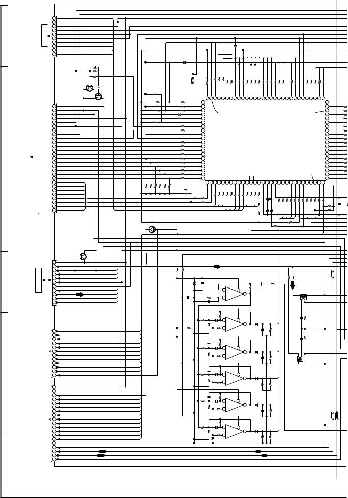
CD-C1W,CP-C1W
A
B
C
D
E
F
G
H
|
CNP201 |
|
|
|
DISPLAYPWB |
|
10 |
RESET |
|
|
GND(D) |
|
||
|
9 |
|
||
|
GND(D) |
|
||
C-1P36 CNS701 |
8 |
|
||
COM1 |
+B |
|||
|
|
7 |
+4.6V(D) |
|
|
|
+12V(M) |
+B |
|
|
|
6 |
||
|
|
+12V(M) |
+B |
|
|
|
5 |
||
|
|
DATA1 |
|
|
|
|
4 |
|
|
|
|
|
|
|
TO |
|
3 |
SCK1 |
|
|
2 |
|
||
|
STB1 |
|
||
|
|
|
|
|
|
|
1 |
|
|
1 1
CD SERVO PWB |
P35 7-H |
|
|
|
|
|
|
|
|
|
|
||
|
|
|
|
|
||
|
|
|
|
|
||
|
|
|
|
|
||
|
|
|
|
|
||
|
|
|
|
|
||
|
|
|
|
|
||
|
|
|
|
|
||
|
|
|
|
|
||
|
|
|
|
|
||
|
|
|
|
|
||
CFW1 |
|
|
|
|
||
|
|
|
|
|||
|
|
|
|
|||
|
|
|
|
|||
|
|
|
|
|||
|
|
|
|
|
||
|
|
|
|
|
|
|
TO |
|
|
|
|
|
|
|
|
|
|
|
|
|
|
|
|
|
|
|
|
|
|
|
|
|
|
|
|
|
|
|
|
|
|
|
|
|
|
|
|
|
|
|
|
|
|
|
|
|
|
|
|
|
|
|
|
|
|
|
|
|
|
|
|
|
|
|
|
|
|
|
|
|
|
|
|
27 27 FW1
CD R-CH
27
GND(Au)
26
CD L-CH
25
GND(D)
24
GND(CD2)
23
+7.3V(CD)
22
+7.3V(CD)
21
GND(4A)
20
PCCC
19
RES
18
SL–
17
SL+
16
RWC
15
CAM_SW1
14
13
CAM_SW2
CAM_SW3
12
CAM_SW4
11
TRY_SW1
10
TRY_SW2
9
TRY_SW3
8
TRY_SW4
7 COIN
6
SQ_OUT
5
CQCK
4
WRQ
3
DRF
2
PIUN
1
CFW2
Q501 GR2SC3199 0V
C207
22/25
R210
47K
R596 CD MUTE
0.7V 2.2K
 R595
R595
0V  2.2K
2.2K
|
0.7V |
Q502 |
2SC3199GR |
0V |
|
||
|
0V |
|
|
+B
TUNER PWB |
P31 11-H |
TO |
|
|
CNP202 |
|
1 |
|
2 |
CNP303 |
3 |
7 |
|
|
4 |
|
5 |
|
6 |
|
8 |
|
9 |
|
10 |
|
11 |
Q204
KTA1266 GR
GND(D)
CL
DO
CE
DI
+12V(A) +B
GND(A)
TUN MUTE
L-CH
R-CH
SD
12P27-B MECHANISMTAPE |
SECTION |
10 |
T1_CROM |
|
|
|
1 |
T2_RUN |
|
|
|
2 |
T1_RUN |
|
|
|
3 |
T2_SOL |
|
|
|
4 |
T1_SOL |
|
|
|
5 |
MOTOR |
|
|
|
T2_B-FP |
|
|
|
|
6 |
|
|
|
|
T2_A-FP |
|
|
|
|
7 |
|
|
|
|
T2_CROM |
|
|
|
|
8 |
|
|
|
|
T2_PLAY |
|
|
|
|
9 |
|
|
|
|
|
|
|
TO |
|
11 |
T1_PLAY |
|
|
HIGH_SP |
|
||
|
12 |
|
||
|
|
13 |
GND(D) |
|
|
|
+12V(A) |
+B |
|
|
|
14 |
||
|
|
HIGH_SP |
|
|
|
|
15 |
|
|
|
|
PB_MUTE |
|
|
|
|
16 |
|
|
D-12 |
SECTION |
TA_R/P |
|
|
21 |
|
|||
|
|
17 |
REC_MUT |
|
|
|
18 |
BEAT_CUT |
|
|
|
19 |
TA_BIAS |
|
|
|
TA_REC EQ |
|
|
|
|
20 |
|
|
|
|
|
|
|
P25 |
DECK |
22 |
DUBB_MOD |
|
D-ON/OFF |
|
|||
|
|
23 |
|
|
|
|
D-PB/REC |
|
|
|
|
24 |
|
|
|
|
TA_PB-EQ |
|
|
|
TO |
25 |
|
|
|
TA_T1/T2 |
|
||
|
26 |
|
||
|
|
GND(A) |
|
|
|
|
27 |
|
|
|
|
REC L-CH |
|
|
|
|
28 |
|
|
|
|
REC R-CH |
|
|
|
|
29 |
|
|
|
|
PRE L-CH |
|
|
|
|
30 |
|
|
|
|
PRE R-CH |
|
|
|
|
31 |
|
|
|
|
|
|
GND(CD2) |
|
|
|
|
GND(CD1) |
|
|
|
|
GND(D) |
|
|
|
|
+7.3V(CD) |
+B |
|
|
+B |
+12V(M) |
+B |
|
|
+B |
+4.6V(D) |
+B |
|
|
+B |
|
+B |
|
|
+4.6V( -CO |
|
|
|
|
GND( -CON |
|
|
|
C208 |
|
|
|
|
0.022 |
+B |
|
|
|
|
|
|
|
|
|
R211 |
|
D206 |
R205 |
|
10K |
|
|
|
||
|
1SS133 |
10K |
|
|
R214
47K
R206 10K
R240 10K
R209 10K
+B
R223 10K |
R224 10K |
R225 10K |
R226 10K |
R227 10K |
Q206 |
|
KRA107 M 4.0V 1 |
3 0.3V |
4.0V |
|
2 |
|
+B |
|
HIGH SP |
|
SELECTOR |
|
|
|
RA801K |
RA781K |
RA771K |
RA761K |
RA751K |
RA741K |
RA731K |
RA721K |
RA711K |
RA701K |
RA691K |
RA681K |
RA671K |
RA661K |
RA651K |
RA641K |
RA631K |
RA621K |
RA611K |
RA591K |
RA581K |
|
|
RA551K |
RA541K |
RA531K |
RA521K |
RA511K |
|
|
|
|
|
||||||||||||||
SW202 |
100/10 |
|
|
|
|
|
|
|
|
|
|
|
|
|
|
|
|
|
|
|
|
|
|
|
|
|
|
|
|
|
|
|
|
|
|
|
|
|
|
|
|
|
|
|
|
|
|
|
||
SPAN |
|
|
|
|
|
|
|
|
|
|
|
|
|
|
|
|
|
|
|
|
|
|
|
|
|
|
|
|
|
|
|
|
|
|
|
|
|
|
|
|
|
|
|
|
|
|
|
|
|
|
|
50/9 |
|
4.0V |
9K/10K |
POWER |
MUTSWFE |
MUTCENT |
MUTREAR |
MUTSYS |
MUTLINE |
CA-VOICE |
DOC2B |
DIC2B |
SDTUN |
CLC2B |
CEC2B |
ENAPL |
STRBQS |
CLQS |
DAQS |
INHSRS |
BSRS |
ASRS 3DSRS PASSSRS |
MUTTUN |
VSS VDD |
MOTOFUN |
RELAYSP |
MUTPB |
PB/REC-D |
ON/OFF-D 0V |
|
|
|
|
||||||||||||||||
|
|
|
RA79 |
|
|
|
|
|
|
|
|
|
|
|
|
|
|
|
|
|
|
|
|
|
|
|
|
|
|
|
|
|
|
|
|
|
|
|
|
|
|
|
|
|
|
|
|
|
||
|
|
|
|
1K |
|
|
|
|
|
|
|
|
|
|
|
|
|
|
|
|
|
|
|
|
|
|
|
|
|
|
|
|
|
|
|
|
|
|
|
|
|
|
|
|
|
|
|
|
|
|
RA81 |
|
0V |
|
80 |
79 |
78 |
77 |
76 |
75 |
74 |
73 |
72 |
71 |
70 |
69 |
68 |
67 |
66 |
65 |
64 |
63 |
62 |
61 |
60 |
59 |
58 |
57 |
56 |
55 |
54 |
53 |
52 |
51 |
|
RA49–RA3 |
|||||||||||||||
1K |
|
MIC_DET |
|
|
|
|
|
|
|
|
|
|
|
|
|
|
|
|
|
|
|
|
|
|
|
|
|
|
|
|
|
|
|
|
|
|
|
|
|
|
|
|
|
|
|
|
||||
|
|
PL6 |
PF7 |
PF6 |
PF5 |
|
|
|
|
|
|
|
|
|
|
|
|
|
|
|
|
|
|
|
|
|
|
|
|
|
|
|
|
|
PD0 |
|
PC5 |
|
0V |
|
|
|||||||||
RA83 1K |
|
TUN_ST |
81 |
PL5 |
PF4 |
|
PF3 |
PF2 |
PF1 |
PF0 |
PE7 |
PE6 |
PE5 |
PE4 |
|
PE3 |
PE2 |
PE1 |
PE0 |
|
PD7 |
PD6 |
PD5 |
PD4 |
PD3 |
|
PD2 |
VSS2 |
VDD2 |
|
|
PD1 |
3.8VPC7 |
PC6PC4 |
50 |
|
3.8V |
|
||||||||||||
|
83 |
PL0 |
|
0V |
4.0V |
4.0V |
|
|
|
|
|
|
.8V3 |
0V |
PC2 |
48 |
TA_T1/T2 |
|||||||||||||||||||||||||||||||||
RA82 1K |
|
82 |
PL4 0V |
|
|
|
4.0V |
3.7V |
|
3.7V |
|
|
4.0V |
|
4.0V |
|
|
4.0V |
|
|
4.0V |
|
|
|
|
|
3.6V |
3.8V |
|
|
|
|
|
|
|
|
|
PC3 49 |
||||||||||||
R207 10K |
AUT_SCAN |
|
|
4.0V |
|
0V |
0V |
0V |
0V |
|
0V |
0V |
|
0V |
0V |
0V |
0V |
0V |
4.0V |
|
0V |
3.8V 3.8V |
REC-EQ |
|
||||||||||||||||||||||||||
84 |
PL1 |
|
4.0V |
|
|
|
|
PC1 47 |
|
|||||||||||||||||||||||||||||||||||||||||
|
|
H/P SW |
|
|
|
|
|
|
|
|
|
|
|
|
|
|
|
|
|
|
|
|
|
|
|
|
|
|
|
|
|
|
|
|
|
|
|
|
|
|
|
|
|
|
|
|
REC_MUT |
|||
R208 10K |
|
SRS_A/NA |
85 |
PL2 |
|
4.0V |
|
|
|
|
|
|
|
|
|
|
|
|
|
|
|
|
|
|
|
|
|
|
|
|
|
|
|
|
|
|
|
|
|
0V |
PC0 46 |
TA_PB-EQ |
||||||||
|
|
DOL_A/NA |
|
|
|
|
|
|
|
|
|
|
|
|
|
|
|
|
|
|
|
|
|
|
|
|
|
|
|
|
|
|
|
|
|
|
TA_R/P |
|
||||||||||||
|
|
86 |
PL3 |
|
0V |
|
|
|
|
|
|
|
|
|
|
|
|
|
|
|
|
|
|
|
|
|
|
|
|
|
|
|
|
|
|
|
|
|
4.0V |
PB7 45 |
|
|||||||||
RA87 1K |
|
CD_MUTE |
|
|
|
|
|
|
|
|
|
|
|
|
|
|
|
|
|
|
|
|
|
|
|
|
|
|
|
|
|
|
|
|
|
|
BEAT_CUT |
|||||||||||||
|
87 |
P30 |
|
3.8V |
|
|
|
|
|
|
|
|
|
|
|
|
|
|
|
|
|
|
|
|
|
|
|
|
|
|
|
|
|
|
|
|
|
0V PB6 44 |
||||||||||||
RA88 1K |
|
|
PCCL |
|
|
|
|
|
|
|
|
|
|
|
|
|
|
|
|
|
|
|
|
|
|
|
|
|
|
|
|
|
|
|
|
|
|
TA_BIAS |
||||||||||||
|
|
88 |
P31 |
|
0V |
|
|
|
|
|
|
|
|
|
|
|
|
|
|
IC201 |
|
|
|
|
|
|
|
|
|
|
|
|
|
|
|
0V |
PB5 43 |
|||||||||||||
|
|
|
VSS |
|
|
|
|
|
|
|
|
|
|
|
|
|
|
|
|
|
|
|
|
|
|
|
|
|
|
|
|
|
|
HIGH_SP |
||||||||||||||||
|
|
|
89 |
VSS3 |
|
0V |
|
|
|
|
|
|
|
|
|
|
|
|
|
|
|
|
|
|
|
|
|
|
|
|
|
|
|
0.3V PB4 |
42 |
|||||||||||||||
RA91 10K |
|
|
VDD |
90 |
VDD3 |
|
4.0V |
|
|
|
|
|
|
|
|
|
|
|
IX0210AW |
|
|
|
|
|
|
|
|
|
|
|
|
4.0V |
PB3 41 |
T1_PLAY |
||||||||||||||||
|
|
RES |
|
|
|
|
|
|
|
|
|
|
|
|
|
|
|
|
|
|
|
|
|
|
|
|
T1_RUN |
|
||||||||||||||||||||||
RA92 10K |
|
|
SL– |
91 |
P32 |
|
4.0V |
|
|
|
|
SYSTEM MICROCOMPUTER |
|
|
|
|
|
4.0V PB2 40 |
T1_SOL |
|
||||||||||||||||||||||||||||||
|
|
92 |
P33 |
|
0V |
|
|
|
|
|
|
|
|
|
|
|
0V PB1 |
39 |
|
|||||||||||||||||||||||||||||||
RA93 10K |
|
|
SL+ |
93 |
P34 |
|
0V |
|
|
|
|
|
|
|
|
|
|
|
|
|
|
|
|
|
|
|
|
|
|
|
|
|
|
|
|
|
|
|
|
|
|
0V |
PB0 38 |
T2_SOL |
|
|||||
RA94 10K |
|
|
RWC |
|
|
|
|
|
|
|
|
|
|
|
|
|
|
|
|
|
|
|
|
|
|
|
|
|
|
|
|
|
|
|
|
|
|
|
MOTOR |
|
||||||||||
|
|
94 |
P35 |
|
0V |
|
|
|
|
|
|
|
|
|
|
|
|
|
|
|
|
|
|
|
|
|
|
|
|
|
|
|
|
|
|
|
|
|
|
0V PA7 37 |
|
|||||||||
RA95 10K |
|
CAM_SW1 |
|
|
|
|
|
|
|
|
|
|
|
|
|
|
|
|
|
|
|
|
|
|
|
|
|
|
|
|
|
|
|
|
|
|
|
VOL SW |
|
|||||||||||
|
95 |
P00 |
|
0V |
|
|
|
|
|
|
|
|
|
|
|
|
|
|
|
|
|
|
|
|
|
|
|
|
|
|
|
|
|
|
|
|
|
|
0V PA6 36 |
|
||||||||||
RA96 10K |
|
CAM_SW2 |
|
|
|
|
|
|
|
|
|
|
|
|
|
|
|
|
|
|
|
|
|
|
|
|
|
|
|
|
|
|
|
|
|
|
|
T2_PLAY |
||||||||||||
|
96 |
P01 |
|
0V |
|
|
|
|
|
|
|
|
|
|
|
|
|
|
|
|
|
|
|
|
|
|
|
|
|
|
|
|
|
|
|
|
|
4.0V |
PA5 35 |
|||||||||||
RA97 10K |
|
CAM_SW3 |
|
|
|
|
|
|
|
|
|
|
|
|
|
|
|
|
|
|
|
|
|
|
|
|
|
|
|
|
|
|
|
|
|
|
T2_RUN |
|
||||||||||||
|
97 |
P02 |
|
0V |
|
|
|
|
|
|
|
|
|
|
|
|
|
|
|
|
|
|
|
|
|
|
|
|
|
|
|
|
|
|
|
|
4.0V |
4.0V PA4 34 |
|
|||||||||||
RA98 10K |
|
CAM_SW4 |
|
|
Si0 |
SCKØ4.0V |
|
SO1 |
|
SI10V |
SCK13.8V |
P16 |
P17 |
INT0 |
RES |
P740V |
|
P75 |
VSS1 |
CF1 |
2.0VCF2 |
VDD14.0V |
AN0 |
AN1 |
AN2 |
0VAN3 |
|
AN4 |
AN50V |
AN60V |
|
0VAN7 |
INT1 |
T1_CROM |
||||||||||||||||
|
100 P06 |
P07 |
SO0 4.0V |
|
|
|
|
|
INT2 |
INT3PA0 |
31 |
|||||||||||||||||||||||||||||||||||||||
|
|
|
|
99 |
P04 |
|
0V |
|
0V |
|
|
0V |
|
|
|
2.0V |
4.0V |
0V |
4.0V |
|
|
0.4V |
|
1.7V |
|
|
|
0V |
0V |
0V |
|
|
0V |
|
|
|
|
|
4.0V |
|
4.0V |
PA2 |
32 |
|
|
|
||||
RA99 10K |
|
TRY_SW1 |
98 |
P03 |
|
0V |
|
|
|
|
|
|
|
|
|
|
|
|
|
|
|
|
|
|
|
|
|
|
|
|
|
|
|
|
|
|
|
|
|
4.0V |
PA3 |
33 |
T2_CROM |
|||||||
R256 10K |
|
TRY_SW2 |
|
P05 |
|
|
|
|
|
|
|
|
|
|
|
|
|
|
|
|
|
|
|
|
|
|
|
|
|
|
|
|
|
|
|
|
|
|
|
|
|
|
PA1 |
T2_A-FP |
||||||
R228 10K |
|
|
0V |
|
1 |
|
2 |
COIN |
SQ OUT |
CQCK |
COM |
DAT |
SCK |
STB |
DS RES |
WRQ |
RES |
DRF |
1KRA14 |
X201 4.19MHz |
CF2 |
VDD |
|
SP63Hz |
SP250Hz |
SP 1K |
SP 4K |
SP16K |
POSISTOR TUNSM |
SPDET |
|
SYSSTOP |
PROTECT |
0V |
T2B-FP |
|
|
4.0V |
|
|
||||||||||
|
|
1K |
|
|
|
|
|
10K |
|
|
||||||||||||||||||||||||||||||||||||||||
R201 10K |
|
|
|
4.0V |
SW3 |
SW4 |
|
|
|
|
|
|
|
|
|
|
|
|
|
|
|
PIUN |
VSS |
CF1 |
|
|
|
|
|
|
|
|
|
|
|
|
|
|
|
|
|
|
|
4.0V |
|
|
|
|
||
R202 10K |
|
|
RA01 |
TRY |
TRY |
|
|
|
|
|
|
|
|
|
|
|
|
|
|
|
|
|
|
|
|
|
|
|
|
|
|
|
|
|
|
|
|
|
|
|
|
|
|
|
|
|
|
|
||
|
|
|
1K |
|
RA031K |
RA041K |
RA051K |
RA061K |
RA071K |
RA081K |
RA091K |
RA101K |
RA111K RA121K |
R204RA131K 10K |
C205 |
C206 |
(CH)15P |
1KRA19 |
1KRA20 1KRA21 1KRA22 |
1KRA23 |
1KRA24 1KRA25 |
1KRA26 |
1KRA27 |
1KRA28 |
RA29 1K |
RA30 |
|
C256 0.022 |
||||||||||||||||||||||
|
|
|
RA02 |
|
4.0V |
1K |
10K |
|
||||||||||||||||||||||||||||||||||||||||||
|
|
|
|
|
|
|
|
|
|
|
|
|
|
|
|
|
|
|
|
|
|
|
|
|
|
|
|
|
|
|
|
|
|
|
|
|
|
|
|
|
|
|
R216 |
|
|
|||||
|
|
|
|
|
|
|
|
|
|
|
|
|
|
|
|
|
|
|
|
|
|
|
|
|
|
|
|
|
|
|
|
|
|
|
|
|
|
|
|
|
|
|
|
|
|
|
|
|||
|
|
|
|
|
|
|
|
|
|
|
|
|
|
|
|
|
|
|
|
|
|
|
|
|
|
|
|
|
|
|
|
|
|
|
|
|
|
|
|
|
|
|
|
|
|
|
|
R258 |
|
|
|
|
|
|
|
|
|
|
|
|
|
|
|
|
|
|
|
|
|
|
|
|
|
|
15P (CH) |
|
|
|
|
|
|
|
|
|
|
|
|
|
|
|
|
|
|
|
|
|
|
|
|||
HIGH SP |
|
|
|
|
|
|
|
|
|
|
|
|
|
|
|
|
|
|
|
|
|
|
|
|
R238 |
|
|
|
R257 |
|
|
|
|
|
|
|
|
|
|
|
|
|
|
|
|
|
|
|||
|
|
|
|
|
|
|
|
|
|
|
|
|
|
|
|
|
|
|
|
|
+B |
|
|
100K |
|
|
|
10K |
|
|
|
|
|
|
|
|
|
|
|
|
|
|
|
|
|
|
||||
GND(A)
|
|
+12V(A) |
|
|
+B |
|
|
|
|
|
|
|
|
–15V |
|
|
–B |
|
|
|
|
|
|
R582 |
|
R583 |
|
|
|
|
|
|
|
|
|
|
220 |
|
|
|
|
|
|
|
|
|
|
330 |
|
|
|
|
|
|
|
|
|
|
|
|
|
|
|
|
|
|
|
|
+B |
|
C560 |
|
|
ZD550 MTZJ5.6A |
0.022 |
|
0V 6 |
– |
8 |
470K |
|||
|
|
|
0.022 |
||||||||
|
|
|
C576 |
|
|
|
|
5.5V |
R554 |
|
|
|
|
|
|
|
|
|
|
|
|
||
|
|
|
R555 |
|
|
|
IC502 |
7 |
|
||
|
|
–B |
270K |
|
0V |
|
(1/2) |
|
|||
|
|
|
|
0V |
|
||||||
|
|
C575 |
C577 |
|
|
|
5 |
+ |
NJM4558MF |
|
|
|
|
0.022 |
0.022 |
|
|
|
|
|
OPE AMP. |
|
|
|
|
–B |
|
|
|
|
|
|
|
|
|
|
|
|
C571 |
|
|
|
R577 |
|
|
|
|
|
|
|
270P |
C572 |
390K |
-11.6V |
|
|
|||
|
|
R578 |
270P |
|
|
|
D556 |
||||
|
|
10K |
2 |
|
4 |
|
|||||
|
|
R558 |
|
|
|
0.5V |
– |
0.4V |
1SS133 |
||
|
|
R579 |
|
|
|
IC503 |
1 |
|
|||
|
+B |
100K |
33K |
|
|
0.5V |
3 |
(1/2) |
|
|
|
|
|
|
|
|
+ |
NJM4558MF C574 |
|||||
|
|
|
|
|
R580 |
||||||
|
|
|
|
|
|
|
|||||
|
|
|
|
|
|
|
OPE AMP. |
2.2/50 |
|||
|
+B |
|
|
|
220K |
|
|
||||
|
|
|
|
|
|
|
|
|
+B |
|
|
|
|
|
|
|
R572 |
|
|
|
|
||
|
|
C569 |
|
|
|
|
|
|
|||
|
|
|
470K |
0.5V |
|
|
5.5V |
|
|||
|
|
680P |
|
|
|
|
|
|
|
D555 |
|
|
|
|
|
|
|
|
6 |
– |
8 |
0.4V |
|
|
|
12K |
C570 |
680P |
|
1SS133 |
|||||
|
|
0.5V |
(1/2) |
7 |
|
||||||
|
|
R573 |
|
|
|
|
IC504 |
|
|
||
|
|
|
R574 |
|
|
R575 |
5 |
+ |
NJM4558MF C573 |
||
|
|
|
39K |
|
|
|
|
||||
|
|
–B |
|
|
|
220K |
|
|
OPE AMP. |
2.2/50 |
|
|
|
C565 |
|
R569 |
|
|
|
|
|
||
|
|
0.0027 |
|
390K |
0.5V |
|
-11.6V |
|
|
||
|
|
|
|
|
|
|
|
|
|
D554 |
|
|
|
|
|
|
|
|
2 |
– |
4 |
|
|
|
|
R567 |
|
C566 |
0.4V |
1SS133 |
|||||
|
|
|
|
IC504 |
1 |
|
|||||
|
|
12K |
|
0.0027 |
(2/2) |
|
|||||
|
|
|
|
|
|||||||
|
|
|
R568 |
|
|
|
3 |
+ |
NJM4558MF |
|
|
|
|
|
68K |
|
R570 |
0.5V |
C568 |
||||
|
+B |
C563 |
|
220K |
OPE AMP. |
2.2/50 |
|||||
|
|
|
R564 |
|
|
|
|
|
|||
|
|
0.0082 |
|
680K |
0.5V |
5.5V |
|
|
|||
|
|
|
|
|
|
|
|
|
|||
|
|
|
|
|
|
|
|
|
|
D553 |
|
|
|
|
|
|
|
|
6 |
– |
8 |
|
|
|
|
R562 |
|
C564 |
0.4V |
1SS133 |
|||||
|
|
|
|
IC503 |
|||||||
|
|
|
|
7 |
|
||||||
|
|
18K |
|
0.0082 |
|
(2/2) |
|
||||
|
|
|
|
|
|
||||||
|
|
|
R563 |
|
R565 |
5 |
+ |
NJM4558MF C567 |
|||
|
|
|
22K |
|
|
|
|||||
|
|
–B |
|
|
220K 0.5V |
OPE AMP. |
2.2/50 |
||||
|
|
C561 |
|
R560 |
|
|
|
|
|
||
|
|
0.0068 |
|
2.2M |
0.5V |
|
|
|
|||
|
|
|
|
|
|
|
|
|
-11.6V |
|
D552 |
|
|
|
|
|
|
|
2 |
– |
4 |
0.4V |
|
|
|
R556 |
|
C562 |
1SS133 |
||||||
|
|
|
|
IC502 |
|
||||||
|
|
|
|
1 |
|
||||||
|
|
56K R557 |
|
0.0068 |
|
(2/2) |
|
||||
|
|
|
3 |
|
|
||||||
|
|
|
470K |
|
|
R559 |
+ |
NJM4558MF |
C559 |
||
|
|
|
|
|
|
|
|||||
|
|
|
D557 |
|
2.2M |
0.5V |
OPE AMP. |
2.2/50 |
|||
|
|
|
1SS133 |
|
|
|
|
|
|
|
|
+
R553 |
R594 |
R593 |
|
|
|
1K |
1K |
|
|
||
15K |
|
|
|||
|
|
|
|
|
|
|
|
MPX.FILTER |
|||
|
|
|
L251 |
|
|
16KHz |
|
C251 |
0.0033 |
R591 |
.2K2 |
SPE-1 |
|
|
|
|
|
R581 |
|
|
|
|
|
100K |
|
|
|
R592 |
2.2K |
|
|
C252 |
0.0033 |
||
4KHz |
|
|
|
|
|
SPE-2 |
|
|
|
|
|
 R576 100K
MPX.FILTER
L252
1KHz SPE-3
 R571 100K
250Hz SPE-4
 R566 100K
63Hz SPE-5
 R561
R561
100K GND(A)
REC L-CH
REC R-CH
PRE L-CH
PRE R-CH
NOTES ON SCHEMATIC DIAGRAM can be found on page 16.
1 |
2 |
3 |
4 |
5 |
6 |
Figure 22 SCHEMATIC DIAGRAM (1/15)
– 22 –
 Loading...