


GSM TELEPHONE
SGH-X820
GSM TELEPHONE |
CONTENTS |
1. |
Safety Precautions |
2. |
Specification |
3. |
Product Function |
4. |
Array course control |
5. |
Exploded View and Parts List |
6. |
Disassembly and Assembly |
|
instructions |
7. |
MAIN Electrical Parts List |
8. |
Block Diagrams |
9. |
PCB Diagrams |
10. Flow Chart of Troubleshooting |
|
11. |
Reference data |

Contents
1. |
Safety Precautions |
|
1-1. Repair Precaution ........................................................................... |
1-1 |
|
1-2. ESD(Electrostatically Sensitive Devices) Precaution ........................... |
1-2 |
|
2. |
Specification |
|
2-1. GSM General Specification .............................................................. |
2-1 |
|
2-2. GSM Tx Power Class ...................................................................... |
2-2 |
|
3. |
Product Function |
|
3-1. Main Function ................................................................................ |
3-1 |
|
4. |
Array course control |
|
Software Downloading |
|
|
4-1. Downloading Binary Files ................................................................ |
4-2 |
|
4-2. Pre-requsite for Downloading .......................................................... |
4-2 |
|
4-3. S/W Downloader Program ............................................................... |
4-3 |
|
5. |
Exploded View and Parts List |
|
5-1. Cellular phone Exploded View ......................................................... |
5-1 |
|
5-2. Cellular phone Part list ................................................................... |
5-2 |
|
6. |
Disassembly and Assembly instructions |
|
6-1. Disassembly .................................................................................. |
6-1 |
|
6-2. Assembly ...................................................................................... |
6-3 |
|
6-3. LCD KIT Disassembly ..................................................................... |
6-6 |
|
6-4. LCD KIT Assembly ......................................................................... |
6-7 |
|
7. |
MAIN Electrical Parts List |
|
8. |
Block Diagrams |
|
9. |
PCB Diagrams |
|

|
Contents |
|
|
|
|
|
|
10. Flow Chart of Troubleshooting |
|
|
|
10-1. Baseband |
|
|
|
10-1-1. Power ON .............................................................................. |
10-1 |
||
10-1-2. Initial .................................................................................... |
10-4 |
||
10-1-3. Sim Part ............................................................................... |
10-6 |
||
10-1-4. Charging Part ........................................................................ |
10-8 |
||
10-1-5. Microphone Part ..................................................................... |
10-9 |
||
10-1-6. Speaker Part ........................................................................ |
10-11 |
||
10-1-7. LCD .................................................................................... |
10-13 |
||
10-1-8. Camera ............................................................................... |
10-16 |
||
10-2. RF |
|
|
|
10-2-1. GSM Receiver........................................................................ |
10-18 |
||
10-2-2. DCS Receiver........................................................................ |
10-19 |
||
10-2-3. PCS Receiver......................................................................... |
10-20 |
||
10-2-4. |
GSM Transmitter................................................................... |
10-23 |
|
10-2-5. |
DCS Transmitter.................................................................... |
10-24 |
|
10-2-6. |
PCS Transmitter.................................................................... |
10-25 |
|
10-2-7. |
Bluetooth Part ...................................................................... |
10-27 |
|
11. Reference data

1. Safety Precautions
1-1. Repair Precaution
●Repair in Shield Box, during detailed tuning. Take specially care of tuning or test,
because specipicty of cellular phone is sensitive for surrounding interference(RF noise).
●Be careful to use a kind of magnetic object or tool,
because performance of parts is damaged by the influence of manetic force.
●Surely use a standard screwdriver when you disassemble this product, otherwise screw will be worn away.
●Use a thicken twisted wire when you measure level.
A thicken twisted wire has low resistance, therefore error of measurement is few.
●Repair after separate Test Pack and Set because for short danger (for example an overcurrent and furious flames of parts etc) when you repair board in condition of connecting Test Pack and tuning on.
●Take specially care of soldering, because Land of PCB is small and weak in heat.
●Surely tune on/off while using AC power plug, because a repair of battery charger is dangerous when tuning ON/OFF PBA and Connector after disassembing charger.
●Don't use as you pleases after change other material than replacement registered on SEC System. Otherwise engineer in charge isn't charged with problem that you don't keep this rules.
1-1
SAMSUNG Proprietary-Contents may change without notice
This Document can not be used without Samsung's authorization

Safety Precautions
1-2. ESD(Electrostatically Sensitive Devices) Precaution
Several semiconductor may be damaged easilly by static electricity. Such parts are called by ESD(Electrostatically Sensitive Devices), for example IC,BGA chip etc. Read Precaution below. You can prevent from ESD damage by static electricity.
●Remove static electricity remained your body before you touch semiconductor or parts with semiconductor. There are ways that you touch an earthed place or wear static electricity prevention string on wrist.
●Use earthed soldering steel when you connect or disconnect ESD.
●Use soldering removing tool to break static electricity. , otherwise ESD will be damaged by static electricity.
●Don't unpack until you set up ESD on product. Because most of ESD are packed by box and aluminum plate to have conductive power,they are prevented from static electricity.
●You must maintain electric contact between ESD and place due to be set up until ESD is connected completely to the proper place or a circuit board.
1-2
SAMSUNG Proprietary-Contents may change without notice
This Document can not be used without Samsung's authorization

2. Specification
2-1. GSM General Specification
|
GSM900 |
EGSM 900 |
DCS1800 |
PCS1900 |
|
|
Phase 1 |
Phase 2 |
Phase 1 |
||
|
|
||||
|
|
|
|
|
|
Freq. Band[MHz] |
890~915 |
880~915 |
1710~1785 |
1850~1910 |
|
Uplink/Downlink |
935~960 |
925~960 |
1805~1880 |
1930~1990 |
|
|
|
|
|
|
|
ARFCN range |
1~124 |
0~124 & |
512~885 |
512~810 |
|
975~1023 |
|||||
|
|
|
|
||
|
|
|
|
|
|
Tx/Rx spacing |
45 MHz |
45 MHz |
95 MHz |
80 MHz |
|
|
|
|
|
|
|
Mod. Bit rate/ |
270.833 kbps |
270.833 kbps |
270.833 kbps |
270.833 kbps |
|
Bit Period |
3.692 us |
3.692 us |
3.692 us |
3.692 us |
|
|
|
|
|
|
|
Time Slot |
576.9 us |
576.9 us |
576.9 us |
576.9 us |
|
Period/Frame |
|||||
4.615 ms |
4.615 ms |
4.615 ms |
4.615 ms |
||
Period |
|||||
|
|
|
|
||
|
|
|
|
|
|
Modulation |
0.3 GMSK |
0.3 GMSK |
0.3 GMSK |
0.3 GMSK |
|
|
|
|
|
|
|
MS Power |
33 dBm~13 dBm |
33 dBm~5 dBm |
30 dBm~0 dBm |
30 dBm~0 dBm |
|
|
|
|
|
|
|
Power Class |
5 pcl ~ 15 pcl |
5 pcl ~ 19 pcl |
0 pcl ~ 15 pcl |
0 pcl ~ 15 pcl |
|
|
|
|
|
|
|
Sensitivity |
-102 dBm |
-102 dBm |
-100 dBm |
-100 dBm |
|
|
|
|
|
|
|
TDMA Mux |
8 |
8 |
8 |
8 |
|
|
|
|
|
|
|
Cell Radius |
35 Km |
35 Km |
2 Km |
- |
|
|
|
|
|
|
2-1

Speclflcation
2-2. GSM Tx Power Class
TX Power |
GSM900 |
|
control level |
||
|
||
|
|
|
5 |
33±2 dBm |
|
|
|
|
6 |
31±2 dBm |
|
|
|
|
7 |
29±2 dBm |
|
|
|
|
8 |
27±2 dBm |
|
|
|
|
9 |
25±2 dBm |
|
|
|
|
10 |
23±2 dBm |
|
|
|
|
11 |
21±2 dBm |
|
|
|
|
12 |
19±2 dBm |
|
|
|
|
13 |
17±2 dBm |
|
|
|
|
14 |
15±2 dBm |
|
|
|
|
15 |
13±2 dBm |
|
|
|
|
16 |
11±3 dBm |
|
|
|
|
17 |
9±3 dBm |
|
|
|
|
18 |
7±3 dBm |
|
|
|
|
19 |
5±3 dBm |
|
|
|
|
|
|
TX Power |
DCS1800 |
|
control level |
||
|
||
|
|
|
0 |
30±3 dBm |
|
|
|
|
1 |
28±3 dBm |
|
|
|
|
2 |
26±3 dBm |
|
|
|
|
3 |
24±3 dBm |
|
|
|
|
4 |
22±3 dBm |
|
|
|
|
5 |
20±3 dBm |
|
|
|
|
6 |
18±3 dBm |
|
|
|
|
7 |
16±3 dBm |
|
|
|
|
8 |
14±3 dBm |
|
|
|
|
9 |
12±4 dBm |
|
|
|
|
10 |
10±4 dBm |
|
|
|
|
11 |
8±4 dBm |
|
|
|
|
12 |
6±4 dBm |
|
|
|
|
13 |
4±4 dBm |
|
|
|
|
14 |
2±5 dBm |
|
|
|
|
15 |
0±5 dBm |
|
|
|
TX Power |
PCS1900 |
|
control level |
||
|
||
|
|
|
0 |
30±3 dBm |
|
|
|
|
1 |
28±3 dBm |
|
|
|
|
2 |
26±3 dBm |
|
|
|
|
3 |
24±3 dBm |
|
|
|
|
4 |
22±3 dBm |
|
|
|
|
5 |
20±3 dBm |
|
|
|
|
6 |
18±3 dBm |
|
|
|
|
7 |
16±3 dBm |
|
|
|
|
8 |
14±3 dBm |
|
|
|
|
9 |
12±4 dBm |
|
|
|
|
10 |
10±4 dBm |
|
|
|
|
11 |
8±4 dBm |
|
|
|
|
12 |
6±4 dBm |
|
|
|
|
13 |
4±4 dBm |
|
|
|
|
14 |
2±5 dBm |
|
|
|
|
15 |
0±5 dBm |
|
|
|
2-2

3. Product Function
Main Function
-Camera and camcorder -Image editor
-Music player -Bluetooth -Photo printing -Phone to TV -Image editor -File viewer -Web browser -Java
-Offline mode
-Multimedia Message Service (MMS) -E-mail
3-1
SAMSUNG Proprietary-Contents may change without notice
This Document can not be used without Samsung's authorization
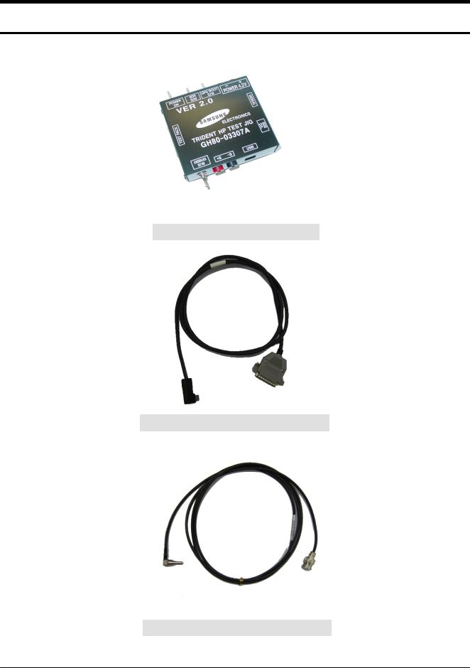
4. Array course control
Test Jig (GH80-03307A)
Test Cable (GH39-00478A)
RF Test Cable (GH39-00182A)
4-1
SAMSUNG Proprietary-Contents may change without notice
This Document can not be used without Samsung's authorization

Array course control
Software Downloading
4-1. Downloading Binary Files
•Three binary files for downloading X820.
–X820XXYY.s3 : Main source code binary.
4-2. Pre-requsite for Downloading
•Downloader Program(OptiFlash.exe)
•X820 Mobile Phone
•Data Cable
•Binary files
4-2
SAMSUNG Proprietary-Contents may change without notice
This Document can not be used without Samsung's authorization
Array course control
4-3. S/W Downloader Program
1. Load the binary download program by executing the “OptiFlash.exe”
2. Select the “Options” -> “Settings” -> “Generic” -> “Specify hardware platform”.
Choose hardware platform for the downloader file setting.
Set the everything else as the default values which are shown below
4-3
SAMSUNG Proprietary-Contents may change without notice
This Document can not be used without Samsung's authorization
Array course control
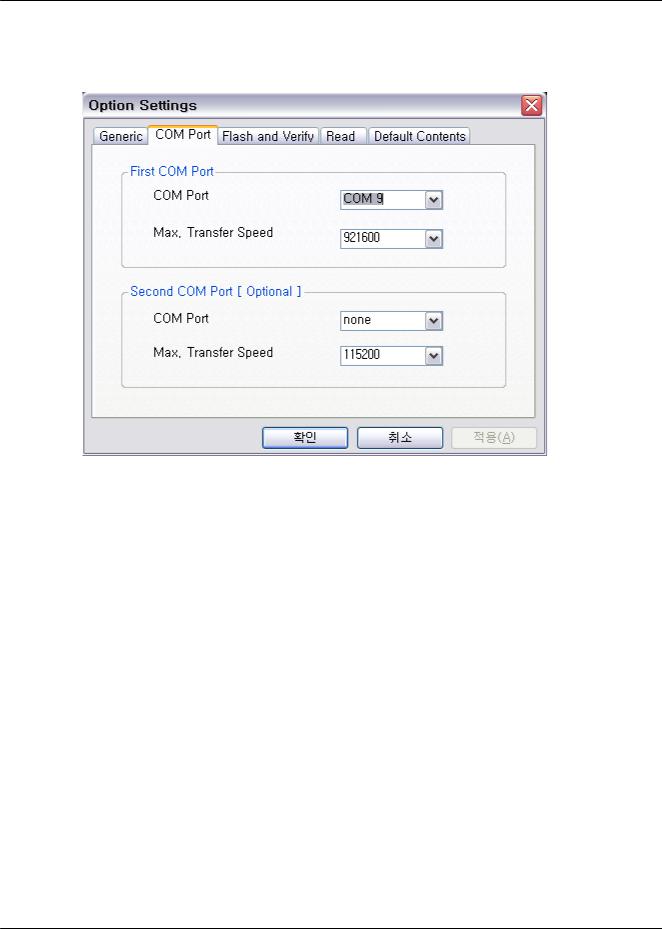
3. Select the COM port when the download cable is connected
Up to twelve ports are supported. Additionally you can select the maximum transfer speed OptiFlash will use to communicate with the phone. However, OptiFlash will use a slower speed if either the PC’s or the phone’s serial hardware is incapable of handling the selected speed
4-4
SAMSUNG Proprietary-Contents may change without notice
This Document can not be used without Samsung's authorization
Array course control
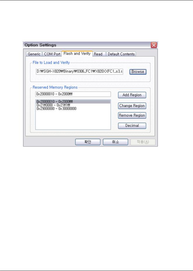
4. Select the“Flash&Verify” -> “Browse”
Set the directory path and choose the latest s/w binary, for example “X820XXYY.s3”, for the downloader binary setting.
Make sure that not to change the reserved memory regions.
In case of X820 the reserved regions are : -0x20000010 – 0x2000ffff
-0x21ff0000– 0x21ff1fff -0x29000000 – 0x30000000
4-5
SAMSUNG Proprietary-Contents may change without notice
This Document can not be used without Samsung's authorization
Array course control
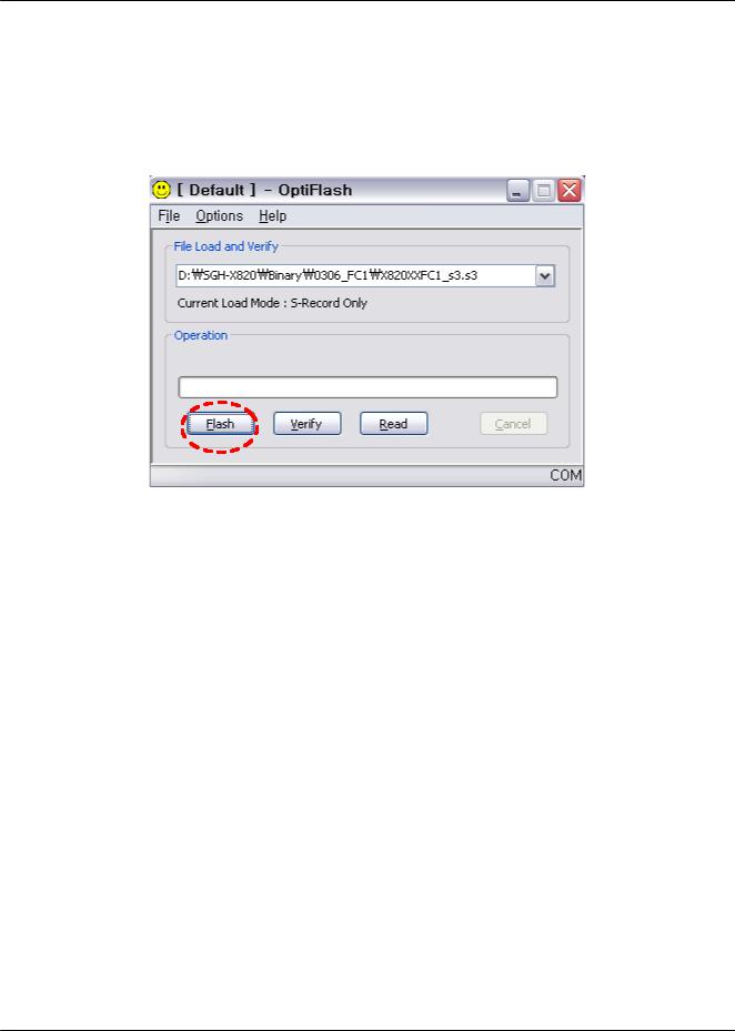
5. Click “OK” button then press “Flash”.
(Before pressing ‘Flash’ button, push the button ‘*’and ‘END’ at the same time. Then press ‘Flash’.)
Downloader will upload the binary file as below for the downloading.
6.When downloading is finished successfully, there is a “All is well” message.
7.After finishing downloading, Certain memory resets should be done to guarantee the normal performance.
8.Confirm the downloaded version name and etc. :
*#1234#
Full Reset :
*2767*3855#
4-6
SAMSUNG Proprietary-Contents may change without notice
This Document can not be used without Samsung's authorization

5. Exploded View and Parts List
5-1. Cellular phone Exploded View
QKP01
QME01
QMI03
QFR01
QCK01
QVO01
QLC01 |
QMI07 |
|
|
|
QCR05 |
|
QMP01 |
QSP02 |
|
QAN02 |
QCA02 |
QVK01 |
|
QCA01 |
|
QRE01 |
QRF03 |
|
QCR06 |
|
QSC01 |
|
QSC02 |
QBA01 |
|
|
QCW01 |
|
QRF01 |
|
|
QBA00 |
5-1
SAMSUNG Proprietary-Contents may change without notice
This Document can not be used without Samsung's authorization

Main Electrical Parts List
5-2. Cellular phone Parts list
Design LOC |
Discription |
SEC CODE |
|
QAN02 |
|
INTENNA-SGHX820 |
GH42-00791A |
QBA00 |
|
PMO-CASE BATTERY |
GH72-29063A |
QBA01 |
|
INNER BATTERY PACK-630MAH,BLK, |
GH43-02386A |
QCA01 |
|
UNIT-CAMERA |
GH59-02950A |
QCA02 |
|
UNIT-CAMERA KEY |
GH59-03026A |
QCK01 |
|
MEC-CAM KEY |
GH75-09582A |
QCR05 |
|
SCREW-MACHINE |
6001-001478 |
QCR06 |
|
SCREW-MACHINE |
6001-001155 |
QCW01 |
|
PMO-COVER WINDOW CAMERA |
GH72-29074A |
QKP01 |
|
MEC-KEYPAD(ZKA/XEF) |
GH75-09583A |
QLC01 |
|
LCD-SGHX820 MODULE |
GH07-00882A |
QME01 |
|
UNIT-EL KEY PBA |
GH59-02966A |
QMI07 |
|
ASSY-CASE-MIC SUB |
GH98-01045A |
QMP01 |
|
PBA MAIN-SGH-X820 |
GH92-02621A |
QRF01 |
|
PMO-COVER RF |
GH72-29064A |
QSC01 |
|
PMO-COVER SCREW L |
GH72-29065A |
QSC02 |
|
PMO-COVER SCREW R |
GH72-29066A |
QSP02 |
|
UNIT-SPK MODULE |
GH59-02958A |
QVK01 |
|
UNIT-VOLUMEKEY |
GH59-03027A |
QVO01 |
|
MEC-VOLUME KEY |
GH75-09581A |
QFR01 |
|
MEC-CASE FRONT |
GH75-09579A |
|
QMI03 |
RMO-COVER MIC HOLDER |
GH73-06452A |
QRE01 |
|
MEC-CASE REAR |
GH75-09580A |
|
QRF03 |
PMO-COVER EAR JACK |
GH72-29073A |
5-2
SAMSUNG Proprietary-Contents may change without notice
This Document can not be used without Samsung's authorization

Main Electrical Parts List
Discription |
SEC CODE |
BAG PE |
6902-000297 |
ADAPTOR-SGHD800 TA(EU) |
GH44-01060A |
UNIT-EARPHONE(BLK) |
GH59-02499A |
LABEL(P)-IMEI |
GH68-01335D |
LABEL(P)-WATER SOAK |
GH68-02026A |
LABEL(P)-WATER SOAK |
GH68-02026A |
MANUAL USERS-EU FRENCH |
GH68-10846A |
LABEL(R)-MAIN(FRANCE) |
GH68-10850A |
BOX(P)-UNIT MAIN(EU) |
GH69-03932A |
CUSHION-CASE TA2 MA4 |
GH69-03934A |
RMO-CHSHION INDUCTOR-2 |
GH73-07097A |
MPR-TAPE LCD FPCB |
GH74-20633A |
MPR-CUSHION INDUCTOR-1 |
GH74-21005A |
MPR-VINYL BOHO REAR |
GH74-21012A |
MPR-VINYL BOHO MAIN WINDOW |
GH74-21905A |
MPR-TAPE SPK CONN |
GH74-22095A |
MPR-TAPE SPK CONN |
GH74-22095A |
MPR-TAPE KEYPAD CONN |
GH74-22098A |
MPR-VINYL BOHO KEYPAD |
GH74-22928A |
MPR-CUSHION INDUCTOR-3 |
GH74-23850A |
MPR-VINYL BOHO LCD |
GH74-24623A |
MPR-VINYL BOHO REAR-2 |
GH74-25033A |
MPR-VINYL BOHO EAR DECO |
GH74-25298A |
AS-LCD WINDOW |
GH81-03179A |
AS-TAPEKEYPAD |
GH81-04637A |
AS-LCD TAPE |
GH81-04638A |
5-3
SAMSUNG Proprietary-Contents may change without notice
This Document can not be used without Samsung's authorization
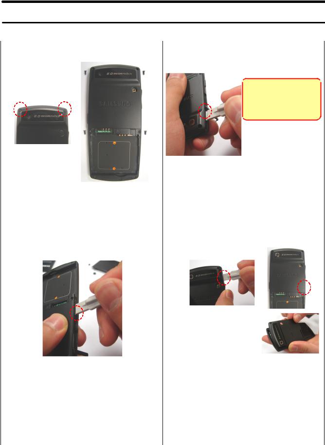
6. Disassembly and Assembly instructions
6-1. Disassembly
1 |
|
2 |
|
 -Please use dismantle
  tool to open
-REAR case is too  soft to be broken
|
|
|
1) |
Press the Rear Camera Hook side with the |
||
1) |
Remove SCREW CAP |
|||||
|
dismantle tool to release the locker |
|||||
2) |
release the screws(4 point) |
|
||||
caution |
||||||
caution |
1) |
Handle the HOOK with care, and check No |
||||
1) |
Handle with care. No scratch |
|
bending the board and front/rear cover |
|||
3 |
|
|
4 |
|
|
|
|
|
|
|
|
|
|
|
|
|
1) |
Press the Rear volume key side (upper and |
|
|
|
|
lower) with the dismantle tool to release |
|
1) |
Press the rear sim connector Hook side |
|
|
|
|
the locker |
||
|
|
with the dismantle tool to release the |
|
|
|
|
|
|
|
|
|
locker |
2) |
Open the rear cover |
|
caution |
caution |
||
|
|
|
||
|
1) |
Handle with care. No scratch |
1) |
Handle with care. No scratch |
|
2) |
Handle the HOOK with care, and check No |
||
|
2) |
Handle the HOOK with care, and check No |
||
|
|
bending the board and front/rear cover |
|
bending the board and front/rear cover |
|
|
6-1 |
|
|
|
|
SAMSUNG Proprietary-Contents may change without notice |
||
This Document can not be used without Samsung's authorization
Disassembly and Assembly instructions
5 |
|
6 |
|
|
|
|
1) |
remove EL SHEET F-PCB |
||
|
|
|
|
CONNECTOR TAPE |
||
|
|
|
2) |
unlock the connector LOCKER and |
||
1) |
Separate CAMERA KEY and VOLUME KEY |
|||||
|
separate key F-PC |
|||||
|
from the cover |
|
||||
|
caution |
|||||
caution |
1) |
FPCB is easy to break and crack |
||||
1) |
FPCB is easy to break and crack |
2) |
Connector is easy to break |
|||
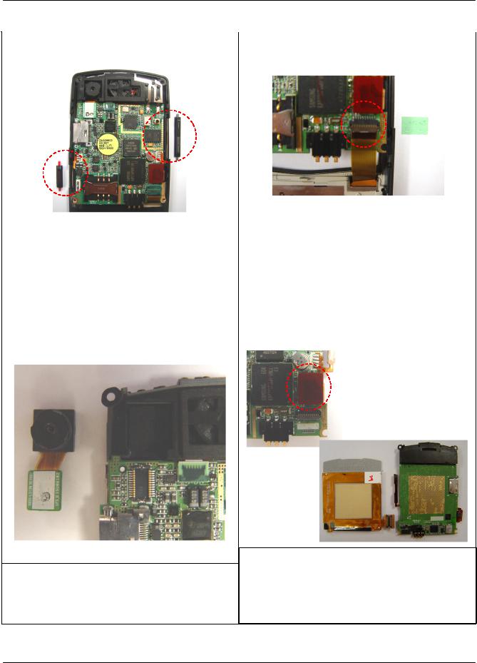
7 |
|
|
8 |
|
||
1)take off the CAMERA CONNECTOR
2)Separate CAMERA MODULE
caution
1) Camera FPCB is easy to break
1)Take off LCD CONNECTOR
2)Separate LCD MODULE
caution
1)LCD glass and LDI are easy to break. Separate LCD module slowly with care
6-2
SAMSUNG Proprietary-Contents may change without notice
This Document can not be used without Samsung's authorization
Disassembly and Assembly instructions
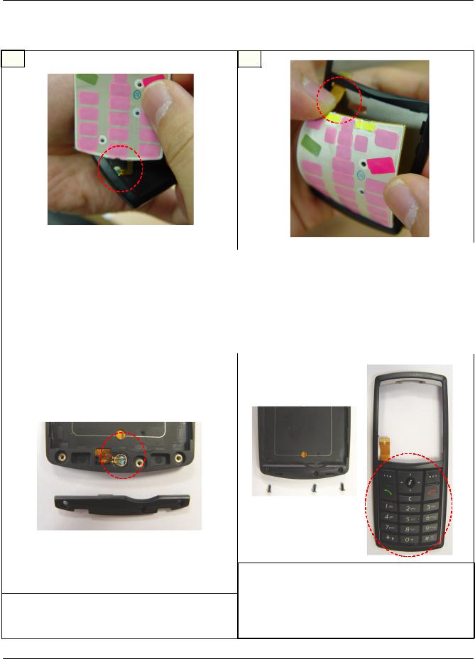
2
|
|
|
1) |
Insert KEY FPCB into the FRONT upper |
||
1) |
Prepare the EL KEY SHEET |
|||||
|
hole |
|||||
2) |
Remove the release paper |
|
||||
2) |
attach a EL KEY PAD to the Front cover |
|||||
3) |
Insert the MIC into the hole of FRONT |
caution |
||||
|
lower hole |
1) |
KEY FPCB has to be inserted before the |
|||
caution |
|
sheet attached. |
||||
1) |
Handle the MIC F-PCB with care. This FPCB |
2) |
Handle the KEY F-PCB with care. This FPCB |
|||
|
tears easily. |
|
tears easily. |
|||
3 |
|
|
4 |
|
|
|
|
|
|
|
|
|
|
1) Place the MIC as the picture below
caution
1) Check the MIC FPCB is OK
1)Put the MIC COVER and CREW
2)Attach KEYPAD
3)Press the KEYPAD not to be detached
caution
1) Check the KEY PAD is OK
6-3
SAMSUNG Proprietary-Contents may change without notice
This Document can not be used without Samsung's authorization
Disassembly and Assembly instructions
5 |
|
6 |
|
|
|
1) |
Combine the module. |
|
|
|
|
||
1) Separated INTENNA ASS'Y and SPEAKER |
caution |
|||
MOTOR MODULE |
1) |
Make sure the FPCB place |
||
7 |
|
8 |
|
|
1)Open the INTENNA ASS'Y F-PCB CONNECTOR LOCKER
2)put the module on the board with checking the PCB guide and FPCB at the same time
caution
1) SPK FPCB has to be inserted to the SILK |
1)Solder INTENNA pad. |
line |
2) Put the blue tape on the connector |
6-4
SAMSUNG Proprietary-Contents may change without notice
This Document can not be used without Samsung's authorization
 Loading...