

Page 1
PIONEER CORPORATION 1-1, Shin-ogura, Saiwai-ku, Kawasaki-shi, Kanagawa 212-0031, Japan
PIONEER ELECTRONICS (USA) INC. P.O. Box 1760, Long Beach, CA 90801-1760, U.S.A.
PIONEER EUROPE NV Haven 1087, Keetberglaan 1, 9120 Melsele, Belgium
PIONEER ELECTRONICS ASIACENTRE PTE. LTD. 253 Alexandra Road, #04-01, Singapore 159936
PIONEER CORPORATION 2012
AVIC-X940BT/XNUC
MULTIMEDIA NAVIGATION RECEIVER
ORDER NO.
CRT4887
AVIC-X940BT
NAVIGATION AV SYSTEM
/XNUC
AVIC-F940BT/XNEU5
AVIC-F840BT/XNEU5
AVIC-F940BT/XNUW5
AVIC-F940BT/XNAU
AVIC-F840BT/XNAU
This service manual should be used together with the following manual(s):
Model No. Order No. Mech.Module Remarks
CX-3283 CRT4843 LS2 DVD Mech. Module : Circuit Descriptions, Mech. Descriptions, Disas-
sembly
K-ZZZ FEB. 2012 Printed in Japan
Page 2
1234
1234
C
D
F
A
B
E
SAFETY INFORMATION
Where in a manufacturer’s service documentation, for example in circuit diagrams or lists
of components, a symbol is used to indicate that a specific component shall be replaced only
by the component specified in that documentation for safety reasons, the following symbol shall
be used:
CAUTION:
USE OF CONTROLS OR ADJUSTMENTS OR PERFORMANCE OF PROCEDURES OTHER THAN THOSE
SPECIFIED HEREIN MAY RESULT IN HAZARDOUS RADIATION EXPOSURE.
- Safety Precautions for those who Service this Unit.
When checking or adjusting the emitting power of the laser diode exercise caution in order to get safe, reliable
results.
Caution:
1. During repair or tests, minimum distance of 13 cm from the focus lens must be kept.
2. During repair or tests, do not view laser beam for 10 seconds or longer.
CAUTION
This product is a class 1 laser product classified under the Safety of laser products, IEC
60825-1:2007, and contains a class 1M laser
module. To ensure continued safety, do not remove any covers or attempt to gain access to
the inside of the product. Refer all servicing to
qualified personnel.
CAUTION—CLASS 1M INVISIBLE LASER
RADIATION WHEN OPEN, DO NOT VIEW
DIRECTLY WITH OPTICAL INSTRUMENTS.
CAUTION
This service manual is intended for qualified service technicians; it is not meant for the casual do-it-yourselfer.
Qualified technicians have the necessary test equipment and tools, and have been trained to properly and safely repair
complex products such as those covered by this manual.
Improperly performed repairs can adversely affect the safety and reliability of the product and may void the warranty.
If you are not qualified to perform the repair of this product properly and safely, you should not risk trying to do so
and refer the repair to a qualified service technician.
W
ARNING
This product may contain a chemical known to the State of California to cause cancer, or birth defects or other reproductive
harm.
Health & Safety Code Section 25249.6 - Proposition 65
2
AVIC-X940BT/XNUC
Page 3

5 678
56
7
8
C
D
F
A
B
E
WARNING!
The AEL (accessible emission level )of the laser power output is less than CLASS 1
but the laser component is capable of emitting radiation exceeding the limit for
CLASS 1.
A specially instructed person should do servicing operation of the apparatus.
Laser diode characteristics
Wave length:
DVD:660 nm to 670 nm
CD:780 nm to 800 nm
Focus lens on Maximum output:
CD:6.26 mW(Emitting period :9 sec.)
DVD:1.27 mW (Emitting period : unlimited)
Additional Laser Caution
Transistors Q1103 and Q1104 in PCB drive the laser diodes for DVD and CD
respectively. When Q1103 or Q1104 is shorted between their terminals,
the laser diodes for DVD or CD will radiate beam. If the top cover is removed
with no disc loaded while such short-circuit is continued, the naked eyes may
be exposed to the laser beam.
AVIC-X940BT/XNUC
3
Page 4

1234
1234
C
D
F
A
B
E
CONTENTS
SAFETY INFORMATION..................................................................................................................................... 2
1. SERVICE PRECAUTIONS............................................................................................................................... 5
1.1 SERVICE PRECAUTIONS ........................................................................................................................ 5
1.2 NOTES ON SOLDERING .......................................................................................................................... 6
2. SPECIFICATIONS............................................................................................................................................ 7
2.1 SPECIFICATIONS ..................................................................................................................................... 7
2.2 DISC/CONTENT FORMAT ...................................................................................................................... 16
3. BASIC ITEMS FOR SERVICE........................................................................................................................ 17
3.1 CHECK POINTS AFTER SERVICING..................................................................................................... 17
3.2 PCB LOCATIONS .................................................................................................................................... 18
3.3 JIGS LIST ................................................................................................................................................ 19
3.4 CLEANING............................................................................................................................................... 20
4. BLOCK DIAGRAM.......................................................................................................................................... 22
4.1 OVERALL CONNECTION DIAGRAM...................................................................................................... 22
4.2 BLOCK DIAGRAM ................................................................................................................................... 24
4.3 POWER SUPPLY SYSTEM FIGURE ...................................................................................................... 38
5. DIAGNOSIS.................................................................................................................................................... 48
5.1 OPERATIONAL FLOWCHART................................................................................................................ 48
5.2 INSPECTION METHOD OF PICKUP UNIT............................................................................................. 49
5.3 DIAGNOSIS FLOWCHART ..................................................................................................................... 52
5.4 ERROR CODE LIST ................................................................................................................................ 72
5.5 CONNECTOR FUNCTION DESCRIPTION............................................................................................. 75
6. SERVICE MODE ............................................................................................................................................ 76
6.1 TEST MODE ............................................................................................................................................ 76
6.2 DVD TEST MODE ................................................................................................................................. 131
7. DISASSEMBLY ............................................................................................................................................ 137
8. EACH SETTING AND ADJUSTMENT ......................................................................................................... 142
8.1 DVD ADJUSTMENT .............................................................................................................................. 142
9. EXPLODED VIEWS AND PARTS LIST........................................................................................................ 148
9.1 PACKING ............................................................................................................................................... 148
9.2 EXTERIOR (1) ....................................................................................................................................... 152
9.3 EXTERIOR (2) ....................................................................................................................................... 154
9.4 EXTERIOR (3) ....................................................................................................................................... 156
9.5 DVD MECHANISM MODULE (1)........................................................................................................... 158
9.6 DVD MECHANISM MODULE (2)........................................................................................................... 160
10. SCHEMATIC DIAGRAM............................................................................................................................. 162
10.1 AV UNIT (PS/IF SECTION)(GUIDE PAGE) ......................................................................................... 162
10.2 AV UNIT (SYSTEM uCOM SECTION)(GUIDE PAGE) ........................................................................ 168
10.3 AV UNIT (AUDIO SECTION)(GUIDE PAGE)....................................................................................... 174
10.4 AV UNIT (TUNER/VICS SECTION)(GUIDE PAGE) ............................................................................ 180
10.5 AV UNIT (FLAP SENSOR IF)(GUIDE PAGE)...................................................................................... 186
10.6 KEYBOARD PCB................................................................................................................................. 192
10.7 DVD CORE UNIT (GUIDE PAGE) ....................................................................................................... 194
10.8 IF PCB (GUIDE PAGE)........................................................................................................................ 200
10.9 MICRO SD PCB................................................................................................................................... 206
10.10 CC MONITOR UNIT(SERVICE)(P/S,I/F SECTION)(GUIDE PAGE).................................................. 208
10.11 CC MONITOR UNIT(SERVICE)(CPU SECTION)(GUIDE PAGE) ..................................................... 214
10.12 CC MONITOR UNIT(SERVICE)(CPU AROUND SECTION)(GUIDE PAGE) .................................... 220
10.13 CC MONITOR UNIT(SERVICE)(DDR/FLASH_ROM/SRAM SECTION)(GUIDE PAGE) .................. 226
10.14 CC MONITOR UNIT(SERVICE)(NAND SECTION)........................................................................... 232
10.15 CC MONITOR UNIT(SERVICE)(VIDEO DEC/T-CON SECTION)(GUIDE PAGE)............................. 234
10.16 CC MONITOR UNIT(SERVICE)(BT/DISPLAY SECTION)(GUIDE PAGE)........................................ 240
10.17 LCD-IF UNIT ...................................................................................................................................... 246
10.18 WAVEFORMS .................................................................................................................................... 248
11. PCB CONNECTION DIAGRAM.................................................................................................................. 250
11.1 AV UNIT ............................................................................................................................................... 250
11.2 KEYBOARD PCB ..............................................................................................................
1.3 DVD CORE UNIT................................................................................................................................. 256
1
11.4 IF PCB.................................................................................................................................................. 258
11.5 MICRO SD PCB ................................................................................................................................... 262
11.6 CC MONITOR UNIT(SERVICE)........................................................................................................... 264
11.7 LCD-IF UNIT ........................................................................................................................................ 268
12. ELECTRICAL PARTS LIST ........................................................................................................................ 270
................... 254
4
AVIC-X940BT/XNUC
Page 5
5 678
56
7
8
C
D
F
A
B
E
1. You should conform to the regulations governing the product (safety, radio and noise, and other regulations), and
should keep the safety during servicing by following the safety instructions described in this manual.
2. Be careful in handling ICs. Some ICs such as MOS type are so fragile that they can be damaged by electrostatic
induction.
3. Please be sure to conduct line process to original status if you make assembling after repair.
4. Please be careful of not to imply static charge onto integrated circuits, etc, when you conduct repair work.
Especially, please use soldering iron with its tip grounded.
Also, please use a pair of tweezers with static charge protection capability if there is the possibility of contacting to
device terminals, and avoid the use of metal-made tweezers.
5. Before disassembling the unit, be sure to turn off the power. Unplugging and plugging the connectors during power-on
mode may damage the ICs inside the unit.
6. To protect the pickup unit from electrostatic discharge during servicing, take an appropriate treatment (shorting-solder)
by referring to "the DISASSEMBLY".
7. Please keep the distance of more than 13 cm from focus lens for safety when you check pickup and make adjustment,
and do not look straight at Laser Beam for more than 10 seconds.
8. Please power adjustment when you replaced mechanical area of DVD Mecha Module or DVD core unit.
9. Graphically-illustrated areas become hot. Be careful not to burn yourself.
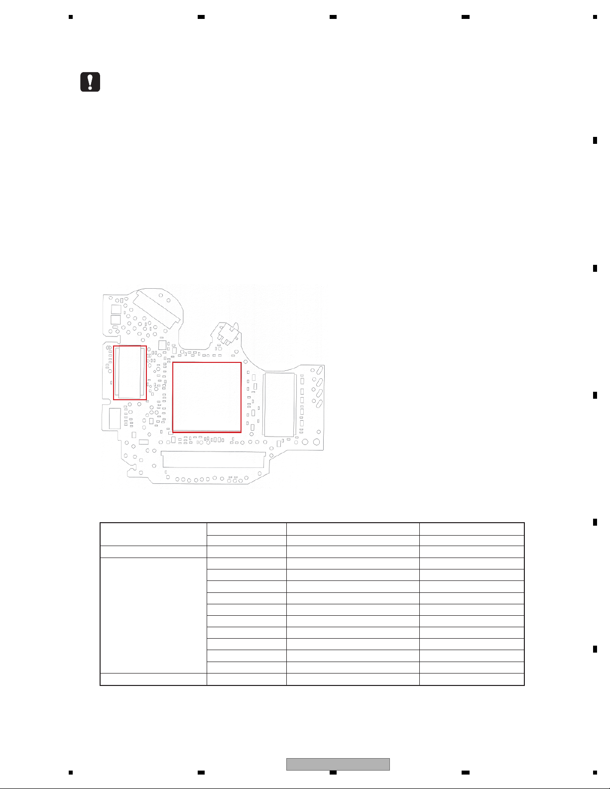
Main IC
IC1501
Drive
IC
IC1251
10. The part listed below is difficult to replace as a discrete component part.
When the part listed in the table is defective, replace whole Assy.
11. On this mechanism, Pickup and Spindle Motor can not be replaced at the service site, because a special facility is
required for the adjustment after replacing them.
So, if Pickup or Spindle Motor is defective, replace the Mechanism Unit.
IF PCB
LCD-IF UNIT
AV UNIT
CC MONITOR UNIT
IC151 GRF3I-0336S Heat pad
IC4204, IC4205 LTC3412AEFE Heat pad
IC5001 R1290K103A Heat pad
IC4001 TT4421 BGA
IC4654 WM1616LGEFL Terminal is bent inside
IC4501 PEM002C8 BGA
IC4901 TC90192XBG BGA
IC4406 CY62147EV30LL45BVA BGA
IC4403 CXX4262 BGA
IC3200 OZ527IRN Heat pad
IC4701 341S2162 Terminal is bent inside
IC5513 AK8859VN Terminal is bent inside
IC1281 LT3505EDD Heat pad
IC2141 LT1912EMSE Heat pad
1. SERVICE PRECAUTIONS
1.1 SERVICE PRECAUTIONS
AVIC-X940BT/XNUC
5
Page 6
1234
1234
C
D
F
A
B
E
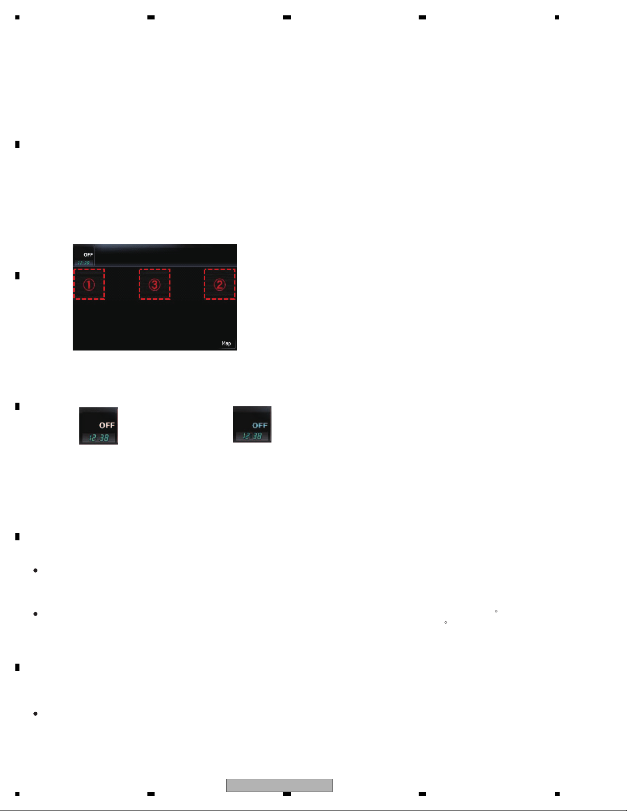
< Procedure >
Top Menu -> AV Source -> Source OFF
Short push area "1" -> Short push area "2" -> Long push area "3" on above screen.
(In order to change the status, follow the same operation.)
The current status can be confirmed by "OFF" character color.
Eject Lock: ON
(Blue character)
Eject Lock: OFF
(White character)
11 33
22
12. Notes on the temperature protection
The temperature protection is set considering the use temperature range of eNAND.
If the temperature reaches the detection temperature shown below, the operation stops (ASENS is disabled).
Detection temperature on low temperature side: -25°C, return temperature: -20°C
Detection temperature on high temperature side: 86.5°C, return temperature: 80°C
13. Control of FAN
There is the control of STOP, low rotation and high rotation.
The temperature (eNAND, DVD mechanism) are detected and controlled it.
14. Pay attention to the wiring of BT cable. (It affects the sensitivity of BT antenna)
15. EJECT LOCK MODE for DVD mechanism
In order to change the EJECT LOCK/UNLOCK status of the mechanism, please perform following procedure.
For environmental protection, lead-free solder is used on the printed circuit boards mounted in this unit.
Be sure to use lead-free solder and a soldering iron that can meet specifications for use with lead-free solders for repairs
accompanied by reworking of soldering.
Compared with conventional eutectic solders, lead-free solders have higher melting points, by approximately 40 C.
Therefore, for lead-free soldering, the tip temperature of a soldering iron must be set to around 373 C in general, although
the temperature depends on the heat capacity of the PC board on which reworking is required and the weight of the tip of
the soldering iron.
Compared with eutectic solders, lead-free solders have higher bond strengths but slower wetting times and higher melting
temperatures (hard to melt/easy to harden).
The following lead-free solders are available as service parts:
Parts numbers of lead-free solder:
GYP1006 1.0 in dia.
GYP1007 0.6 in dia.
GYP1008 0.3 in dia.
1.2 NOTES ON SOLDERING
6
AVIC-X940BT/XNUC
Page 7

5 678
56
7
8
C
D
F
A
B
E
General
Rated power source...............14.4 V DC
(allowable voltage range:
10.8 V to 15.1 V DC)
Grounding system..................Negative type
Maximum current consumption
..........................................10. 0 A
Dimensions (W × H × D):
AVIC-X940BT
Chassis.....................178mm × 100 mm ×
165 mm
(7 in. × 3-7/8 in. × 6-1/2 in.)
Nose...........................170 mm × 96 mm × 12 mm
(6-3/4 in. × 3-3/4 in. ×
1/2 in.)
Weight:
AVIC-X940BT....................1.87 kg (4.1 lbs)
NAND flash memory .............4 GB
Navigation
GPS receiver:
System ...............................L1, C/Acode GPS
SPS (Standard Positioning
Service)
Reception system..........32-channel multi-channel
reception system
Reception frequency.... 1 575.42MHz
Sensitivity ......................... –140 dBm (typ)
Position update frequency
.........................................Approx. once per second
GPS antenna:
Antenna ............................Micro strip flat antenna/
right-handed helical polari-
zation
Antenna cable.................3.55 m (11 ft. 7 in.)
Dimensions (W × H × D)
......................................... 33 mm × 14 .7 mm × 36 m m
(1-1/4 in. × 4/7 in. ×
1-3/8 in.)
Weight ...............................73.7 g (0.211lbs)
Display
Screen size/aspect ratio:
AVIC-X940BT................... 6.1 i nch w ide /16:9
Effective display area:
AVIC-X940BT....................136.2 mm × 72 mm
Pixe ls ........................................... 3 84 00 0 (80 0 × 480)
Di spl ay m eth od ....................... T FT A cti ve ma tri x dr ivi ng
Ba ckl ight .................................... LED
Color system.............................N TSC c omp atibl e
Tolerable temperature range:
Pow er on ........................... +1 4 °F to +140 °F
Pow er of f ...........................–4 °F t o +17 6 °F
Angle adjustment
AVIC-X940BT................... 0°
Audio
Maximum power output .......50 W × 4
50 W × 2 ch/4 Ω +70W×
1 ch/2 Ω (for subwoofer)
Continuous power output ...22 W × 4 (50Hz to 15 kHz,
5 %THD, 4 Ω LOAD, Both
Channels Driven)
Load impedance ..................... 4 Ω (4 Ω to 8 Ω [2 Ω for 1 ch]
allowable)
Preout output level (max):
AVIC-X940BT................... 2. 2 V
Preout impedance:
AVIC-X940BT....................1 kΩ
Equalizer (8-Band Graphic Equalizer):
Frequency......................... 40 Hz /80 H z/2 00 Hz /40 0 Hz/
1 kHz/2.5 kHz/8 kHz/10 kHz
Ga in .....................................±12 dB
Loudness contour:
Lo w ......................................+3.5 dB (100Hz), +3 dB
(10 kHz)
Mi d ......................................+ 10 dB ( 100 Hz ), +6 .5 dB
(10 kHz)
Hi gh ....................................+1 1 dB (10 0 Hz) , +11 d B
(10 kHz)
(volume:–30 dB)
HPF:
Frequency......................... 50 Hz /63 H z/8 0 Hz/ 100 H z/
125 Hz
Sl ope ...................................–12 d B/o ct
Subwoofer:
Frequency......................... 50 Hz /63 H z/8 0 Hz/ 100 H z/
125 Hz
Sl ope ...................................–18 d B/o ct
Ga in .....................................–2 4/+6 dB
Ph ase ................................. Nor mal/Reverse
Bass boost:
Ga in .................................... 0 d B to +1 2 dB
Backup current ........................ 3 mA or less
• AVIC-X940BT/XNUC
2. SPECIFICATIONS
2.1 SPECIFICATIONS
AVIC-X940BT/XNUC
7
Page 8
1234
1234
C
D
F
A
B
E
DVD Drive
System ........................................ DVD-Video, CD, MP3, WMA,
AAC, DivX system
Usable discs .............................DVD-Video, DVD-R(DL),
DVD-RW, CD-ROM, CD-DA,
CD-R/RW
Region number .......................1
Signal format:
Sampling frequency.....44.1 kHz/48 kHz/96 kHz
Number of quantization bits
..........................................16 bit/20 bit/24bit; linear
Frequency response.............. 5Hz to 44 000Hz (with DVD,
at sampling frequency
96 kHz)
Signal-to-noise ratio.............. 97 dB (1kHz) (IHF-A net-
work)
(CD: 96 dB (1 kHz) (IHF-A
network))
Dynamic range ........................95 dB (1kHz) (CD: 94 dB
(1 kHz))
Distortion ................................... 0.008 % (1kHz)
Output level:
Video.................................. 1.0Vp-p/75 Ω (±0.2 V)
Audio ................................. 1.0V (1 kHz, 0dB)
Number of channels ............. 2 (stereo)
MP3 decoding format ...........MPEG-1, 2 & 2.5 Audio Layer
3
WMA decoding format ......... Ver. 7, 8 & 9
AAC decoding format............MPEG-4 AAC (only encoded
by iTunes):
.m4a
DivX decoding format............Home Theater Ver.3.11,
Ver.4.X, Ver.5.X, Ver.6.X:
.avi, .divx
USB
USB standard spec................USB 2.0 High Speed
Max current supply.................1A
File system................................ FAT16, FAT32
USB class.................................. Mass storage class
Decoding format ..................... MP3/WMA/AAC/WAVE/
H.264/MPEG4/WMV
SD (AVIC-X940BT)
microSD card, microSDHC card
Compatible physical format
......................................... Ve rsion 2 .00
Fi le s yst em....................... FAT 16, FAT3 2
De cod ing f ormat ............ MP3 /WMA/AAC/WAVE/
H.264/MPEG4/WMV
Bluetooth
Ver sio n........................................ Blu eto oth 2 .0+ EDR
Ou tpu t po wer ........................... +4 d Bm Ma x.
(Power class 2)
FM tuner
AVIC-X940BT
Fre que ncy r ang e............87 .9 MH z to 10 7.9 M Hz
Us abl e se nsi tiv ity ...........9 dBf ( 0.8 µ V/7 5 Ω, mono,
S/N: 30 dB)
Si gna l-to- noi se ra tio ..... 72 dB (IHF-A network)
Di sto rtion .......................... 0.3 % (a t 65 dB f, 1 k Hz,
stereo)
0.1 % (at 65 dBf, 1 kHz,
mono)
Fre que ncy r esp ons e..... 30 Hz to 1 5 000 Hz ( ±3 dB )
St ere o se par ati on.......... 45 d B (at 6 5 dBf, 1 kHz )
AM tuner
AVIC-X940BT
Fre que ncy r ang e............53 0 kHz t o 1 7 10 kH z
(10 kHz)
Us abl e se nsi tiv ity ...........25 µV (S/N: 20 dB)
Si gna l-to- noi se ra tio ..... 62 dB (IHF-A network)
CEA2006 Specifications
Power output ............................1 4 W R MS × 4 Channels
(4 Ω and
1 % THD+N)
S/N ratio ..................................... 9 1 dBA (reference: 1 W into
4 Ω)
Note
Specifications and design are subject to possible
modifications without notice due to improvements.
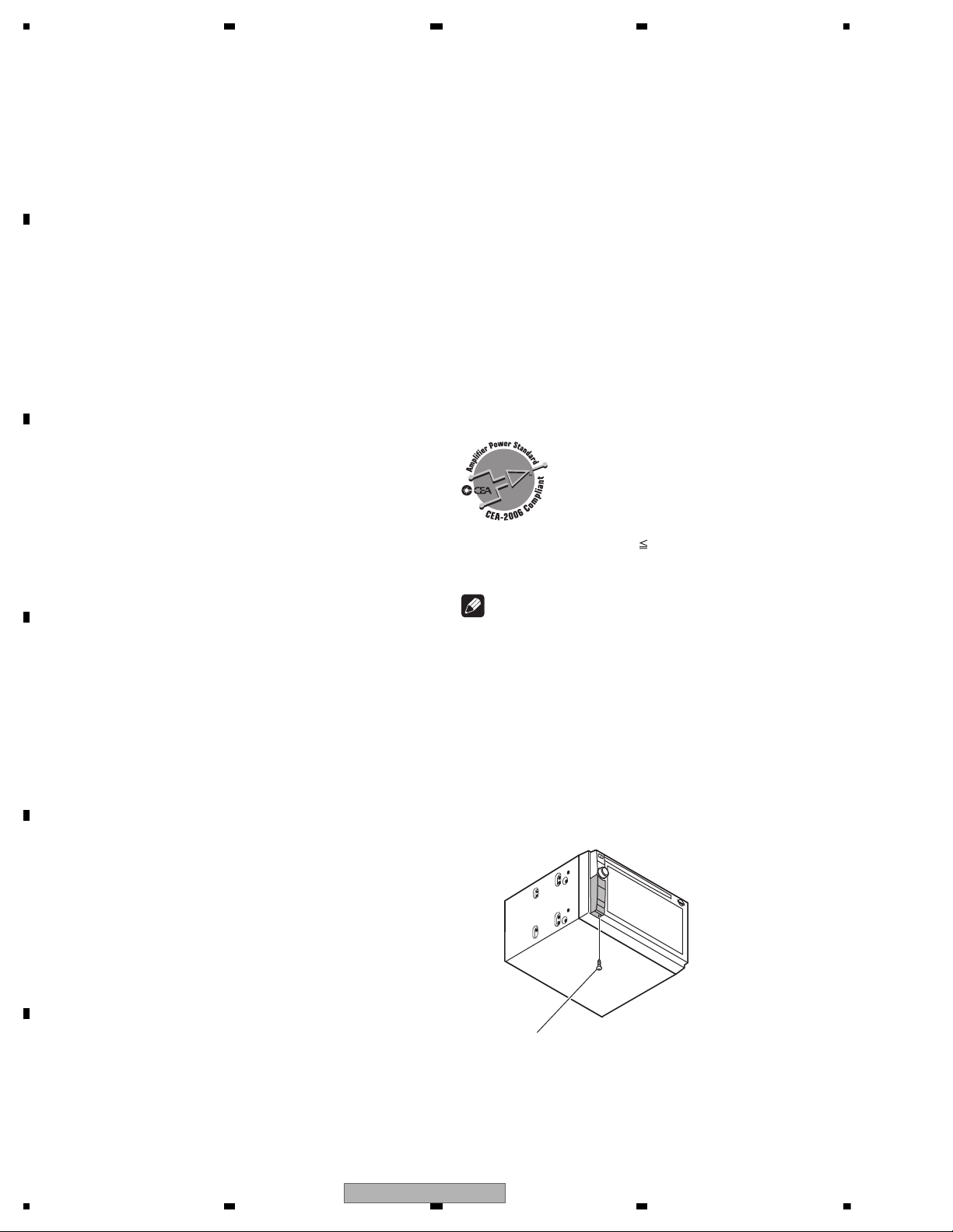
Fastening the detachable faceplate
• This description is for AVIC-X940BT.
If you do not plan to remove the detachable faceplate, the detachable faceplate can be fastened with the supplied screw.
Screw : BPZ20P040FTC (2 mm × 4 mm) (UC)
8
AVIC-X940BT/XNUC
Page 9

5 678
56
7
8
C
D
F
A
B
E
• AVIC-F940BT/XNEU5, AVIC-F840BT/XNEU5
General
Rated power source...............14.4 V DC
(allowable voltage range:
12.0 V to 14.4 V DC)
Earthing system ......................Negative type
Maximum current consumption
......................................... 10. 0 A
Dimensions (W × H × D):
AVIC-F940BT
DIN
Chassis.....................18 8 mm × 118 mm ×
157 mm
Nose...........................170 mm × 96 mm × 2 0 mm
D
Chassis.....................17 8 mm × 100 mm ×
165 mm
Nose...........................170 mm × 96 mm × 1 2 mm
AVIC-F840BT
DIN
Chassis.....................18 8 mm × 118 mm ×
157 mm
Nose...........................170 mm × 96 mm × 2 0 mm
D
Chassis.....................17 8 mm × 100 mm ×
165 mm
Nose...........................170 mm × 96 mm × 1 2 mm
Weight:
AVIC-F940BT................... 2 .4 kg
AVIC-F840BT................... 2 .4 kg
NAND flash memory ............ 4 G B
Navigation
GPS receiver:
Sy ste m............................... L1 , C/Acode GPS
SPS (Standard Positioning
Service)
Reception system..........32-channel multi-channel
reception system
Reception frequency.... 1 575.42 MHz
Sensitivity ......................... –1 40 dB m (typ)
Position update frequency
......................................... Approx. once per second
GPS aerial:
Ae ria l .................................. Mic ro strip flat aerial/right-
handed helical polarisation
Ae ria l ca ble ..................... 3. 55 m
Dimensions (W × H × D)
......................................... 33 mm × 14.7 mm × 36 mm
Wei ght ............................... 73. 7 g
Display
Screen size/aspect ratio:
AVIC-F940BT................... 6 .1 in ch wi de/ 16: 9
AVIC-F840BT................... 6 .1 in ch wi de/ 16: 9
Effective display area:
AVIC-F940BT....................1 36. 2 mm × 72 mm
AVIC-F840BT....................1 36. 2 mm × 72 mm
Pixe ls ........................................... 3 84 00 0 (80 0 × 480 )
Di spl ay m eth od ....................... T FT A cti ve ma tri x dr ivi ng
Backlight ................................... L ED
Co lou r sy ste m ..........................PA L/NTSC compatible
Tolerable temperature range:
Pow er on ........................... –10 °C t o +60 °C
Pow er of f ...........................–2 0 °C to +8 0 °C
Angle adjustment
AVIC-F940BT................... 0 °
AVIC-F840BT................... 0 °
Audio
Ma xim um p owe r out put ....... 50 W × 4
50 W × 2 ch/4 Ω +70W×
1 ch/2 Ω (for subwoofer)
Continuous power output ...22 W × 4 (50Hz to 15 kHz,
5 %THD, 4 ΩLOAD, Both
Channels Driven)
Lo ad im ped ance ..................... 4 Ω (4 Ω to 8 Ω [2 Ω for 1 ch]
allowable)
Preout output level (max):
AVIC-F940BT................... 2 .2 V
AVIC-F840BT................... 2 .2 V
Preout impedance:
AVIC-F940BT....................1 kΩ
AVIC-F840BT....................1 kΩ
Equaliser (8-Band Graphic Equaliser):
Fre que ncy .........................4 0 Hz/8 0 Hz/ 200 H z/4 00 Hz /
1 kHz/2.5 kHz/8 kHz/10 kHz
Ga in .....................................±12 dB
Loudness contour:
Lo w ......................................+3. 5 dB (10 0 Hz) , +3 dB
(10 kHz)
Backup current ....................... 3 mA or less
AVIC-X940BT/XNUC
9
Page 10

1234
1234
C
D
F
A
B
E
Mid ......................................+10 dB (100 Hz), +6.5dB
(10 kHz)
High ....................................+11 dB (100 Hz), +11 dB
(10 kHz)
(volume:–30 dB)
HPF:
Frequency......................... 50 Hz/63Hz/80 Hz/100Hz/
125 Hz
Slope.................................. –12 dB/oct
Subwoofer:
Frequency......................... 50 Hz/63Hz/80 Hz/100Hz/
125 Hz
Slope.................................. –18 dB/oct
Gain .................................... –24/+6dB
Phase ................................ Normal/Reverse
Bass boost:
Gain .................................... 0 dB to +12 dB
DVD Drive
System ........................................ DVD-Video, CD, MP3, WMA,
AAC, DivX system
Usable discs ............................ DVD-Video, DVD-R(DL),
DVD-RW, CD-ROM, CD-DA,
CD-R/RW
Region number .......................2
Signal format:
Sampling frequency.....44.1 kHz/48 kHz/96 kHz
Number of quantisation bits
..........................................16 bit/20 bit/24bit; linear
Frequency response...............5Hz to 44 000Hz (with DVD,
at sampling frequency
96 kHz)
Signal-to-noise ratio...............97 dB (1 kHz) (IEC-A net-
work)
(CD: 96 dB (1 kHz) (IEC-A
network))
Dynamic range ........................95 dB (1kHz) (CD: 94 dB
(1 kHz))
Distortion ................................... 0.008 % (1kHz)
Output level:
Video...................................1.0 Vp-p/75 Ω (±0.2 V)
Audio ..................................1.0 V (1kHz, 0 dB)
Number of channels ............. 2 (stereo)
MP3 decoding format .......... MPEG-1, 2 & 2.5 Audio Layer
3
WMA decoding format ......... Ver. 7, 8 & 9
AAC decoding format............MPEG-4 AAC (only encoded
by iTunes):
.m4a
DivX decoding format............Home Theater Ver.3.11,
Ver.4.X, Ver.5.X, Ver.6.X:
.avi, .divx
USB
USB standard spec................U SB 2.0 H igh S pee d
Max current supply.................1 A
File system................................. FAT16, FAT32
US B cla ss .................................. Ma ss st ora ge cl ass
De cod ing f ormat ..................... MP3 /WM A/AAC/WAVE/
H.264/MPEG4/WMV
SD (AVIC-F940BTand AVIC-F840BT)
microSD card, microSDHC card
Compatible physical format
..........................................Ve rsion 2 .00
File system....................... FAT 16, FAT3 2
De cod ing f ormat ............ MP3 /WMA/AAC/WAVE/
H.264/MPEG4/WMV
Bluetooth
Ver sio n........................................ Blu eto oth 2 .0+ EDR
Ou tpu t po wer ........................... +4 d Bm Ma x.
(Power class 2)
FM tuner
Fre que ncy r ang e..................... 87 .5 MH z to 10 8.0 MH z
Us abl e se nsi tiv ity .................... 9 dBf ( 0.8 µV /75 Ω, mono,
S/N: 30 dB)
Si gna l-to- noi se ra tio ...............72 dB (IEC-A network)
Di sto rtion .................................... 0.3 % (a t 65 dBf, 1 kH z,
stereo)
0.1 % (at 65 dBf, 1 kHz,
mono)
Fre que ncy r esp ons e.............. 3 0 Hz to 1 5 000 Hz ( ±3 dB)
St ere o se par ati on................... 45 dB (a t 65 dB f, 1 k Hz)
MW tuner
Fre que ncy r ang e..................... 53 1 kHz to 1 60 2 kHz ( 9 kHz )
Us abl e se nsi tiv ity .................... 25 µV (S/N: 20 dB)
Si gna l-to- noi se ra tio ...............62 dB (IEC-A network)
LW tuner
Fre que ncy r ang e......................15 3 kHz to 2 81 kH z
Us abl e se nsi tiv ity .................... 28 µV (S/N: 20 dB)
Si gna l-to- noi se ra tio ...............62 dB (IEC-A network)
RDS-TMC tuner
Rated power source...............1 3.8 V D C
(allowable voltage range:
10.0 V to 14.5 V DC)
Earthing system ...................... Negative type
Maximum current consumption
..........................................60 mA
Dimensions (W × H × D) ...68 mm × 49 mm × 19mm
Weight .........................................18 0 g
Note
Specifications and design are subject to possible
modifications without notice due to improvements.
10
AVIC-X940BT/XNUC
Page 11

5 678
56
7
8
C
D
F
A
B
E
• AVIC-F940BT/XNUW5
General
Rated power source...............14.4 V DC
(allowable voltage range:
12.0 V to 14.4 V DC)
Earthing system ......................Negative type
Maximum current consumption
......................................... 10. 0 A
Dimensions (W × H × D):
DIN
Chassis..............................188 mm × 118mm ×
157 mm
Nose....................................170 mm × 96 mm × 20 mm
D
Chassis..............................178 mm × 100mm ×
165 mm
Nose....................................170 mm × 96 mm × 12 mm
Weight ........................................ 2.4 kg
NAND flash memory .............4 GB
Navigation
GPS receiver:
System ...............................L1, C/Acode GPS
SPS (Standard Positioning
Service)
Reception system..........32-channel multi-channel
reception system
Reception frequency.... 1 575.42MHz
Sensitivity ......................... –140 dBm (typ)
Position update frequency
.........................................Approx. once per second
GPS aerial:
Aerial ..................................Micro strip flat aerial/right-
handed helical polarisation
Aerial cable .....................3.55 m
Dimensions (W × H × D)
......................................... 33 mm × 14 .7 mm × 3 6 mm
Weight ...............................73.7 g
Display
Screen size/aspect ratio.......6.1 inch wide/16:9
(effective display area:
136.2 mm × 72 mm)
Pixels ........................................... 384 000 (800 × 480)
Display method ....................... TFT Active matrix driving
Backlight ................................... LED
Colour system.......................... PAL/NTSC/SECAM compati-
ble
Tolerable temperature range:
Power on.......................... –10°C to +60 °C
Power off.......................... –20°C to +80 °C
Audio
Maximum power output .......50 W × 4
50 W × 2 ch/4 Ω +70W×
1 ch/2 Ω (for subwoofer)
Continuous power output ...22 W × 4 (50Hz to 15 kHz,
5 %THD, 4 Ω LOAD, Both
Channels Driven)
Load impedance ..................... 4 Ω (4 Ω to 8 Ω [2 Ω for 1 ch]
allowable)
Preout output level (max) ....2.2 V
Preout impedance ..................1 kΩ
Equaliser (8-Band Graphic Equaliser):
Fre que ncy .........................40 H z/8 0 Hz/ 200 H z/4 00 Hz /
1 kHz/2.5 kHz/8 kHz/10 kHz
Ga in .................................... ±12 dB
Loudness contour:
Lo w ..................................... +3.5 dB (100Hz), +3 dB
(10 kHz)
Mi d ..................................... + 10 dB ( 100 Hz ), +6 .5 dB
(10 kHz)
Hi gh ................................... +1 1 dB (10 0 Hz) , +11 dB
(10 kHz)
(volume:–30 dB)
HPF:
Frequency......................... 50 Hz /63 H z/8 0 Hz/ 100 H z/
125 Hz
Sl ope .................................. –12 d B/o ct
Subwoofer:
Frequency......................... 50 Hz /63 H z/8 0 Hz/ 100 H z/
125 Hz
Sl ope .................................. –18 d B/o ct
Ga in .................................... –2 4/+6 dB
Ph ase ................................. Nor mal/Reverse
Bass boost:
Ga in .....................................0 d B to +1 2 dB
DVD Drive
Sy ste m........................................ DVD -Video, CD, MP3, WMA,
AAC, DivX system
Usable discs .............................D VD-Vi deo, DVD-R(DL),
DVD-RW, CD-ROM, CD-DA,
CD-R/RW
Re gio n nu mbe r ....................... 5
Signal format:
Sampling frequency.....44.1 kHz/48 kHz/96 kHz
Number of quantisation bits
......................................... 16 bit/20 bit/24 bit; linear
Frequency response.............. 5 Hz to 4 4 000 H z (with DVD,
at sampling frequency
96 kHz)
Signal-to-noise ratio.............. 9 7 dB (1 kHz ) (IEC-A net-
work)
(CD: 96 dB (1 kHz) (IEC-A
network))
Backup current ....................... 3 mA or less
AVIC-X940BT/XNUC
11
Page 12

1234
1234
C
D
F
A
B
E
Dynamic range ........................95 d B ( 1 kHz ) (C D: 94 dB
(1 kHz))
Distortion ................................... 0.008 % (1kHz)
Output level:
Video................................... 1.0 Vp-p/75 Ω (±0.2 V)
Audio .................................. 1.0 V ( 1 kHz, 0dB)
Number of channels ............. 2 (s tereo)
MP3 decoding format ...........MPEG-1, 2 & 2.5 Audio Layer
3
WMA decoding format .........Ver. 7 , 8 & 9
AAC decoding format............ MPEG-4 AAC (only encoded
by iTunes):
.m4a
DivX decoding format............Home Theater Ver.3.11,
Ver.4.X, Ver.5.X, Ver.6.X:
.avi, .divx
USB
USB standard spec................ USB 2 .0 H igh Speed
Max current supply................. 1 A
File system................................. FAT16, F AT32
USB class.................................. M ass storage class
Decoding format ..................... MP3/WMA/AAC/WAVE/
H.264/MPEG4/WMV
SD
microSD card, microSDHC card
Compatible physical format
................................................... Version 2.00
File system................................. FAT16, F AT32
Decoding format ..................... MP3/WMA/AAC/WAVE/
H.264/MPEG4/WMV
Bluetooth
Version........................................ Bluetooth 2.0+EDR
Output power ........................... +4 d Bm Max.
(Power class 2)
FM tuner
Frequency range..................... 87.5 M Hz to 108.0 MHz
Usable sensitivity.................... 9 dBf ( 0.8 µV/75 Ω, mono,
S/N: 30 dB)
Signal-to-noise ratio............... 72 dB (IEC -A network)
Distortion ................................... 0 .3 % (a t 65 dB f, 1 kHz,
stereo)
0.1 % (at 65 dBf, 1 kHz,
mono)
Frequency response.............. 30 Hz to 1 5 000 Hz ( ±3 dB)
Stereo separation................... 4 5 dB (a t 65 dB f, 1 k Hz)
MW tuner
Frequency range..................... 531 kH z t o 1 602 k Hz (9 kHz)
Usable sensitivity.................... 25 µV (S/N: 20 dB)
Signal-to-noise ratio............... 62 dB (IEC -A network)
LW tuner
Frequency range......................153 kH z t o 28 1 kHz
Usable sensitivity.................... 28 µV (S/N: 20 dB)
Signal-to-noise ratio............... 62 dB (IEC -A network)
Note
Specifications and design are subject to possible
modifications without notice due to improvements.
12
AVIC-X940BT/XNUC
Page 13

5 678
56
7
8
C
D
F
A
B
E
• AVIC-F940BT/XNAU, AVIC-F840BT/XNAU
General
Rated power source...............14.4 V DC
(allowable voltage range:
10.8 V to 15.1 V DC)
Earthing system
...................... Negative type
Maximum current consumption
..........................................10. 0 A
Dimensions (W × H × D):
AVIC-F940BT
D
Chassis.....................17 8 mm × 100 mm ×
165 mm
Nose...........................170 mm × 96 mm × 1 2 mm
AVIC-F840BT
D
Chassis.....................17 8 mm × 100 mm ×
165 mm
Nose...........................170 mm × 96 mm × 1 2 mm
Weight:
AVIC-F940BT....................1 .85 k g
AVIC-F840BT................... 1 .85 k g
NAND flash memory ............ 4 G B
Navigation
GPS receiver:
System .............................. L 1, C /Acode GPS
SPS (Standard Positioning
Service)
Reception system..........32-channel multi-channel
reception system
Reception frequency.... 1 575.42 MHz
Sensitivity ......................... –1 40 dB m (typ)
Position update frequency
..........................................Approx. once per second
GPS aerial:
Aerial .................................. Micro strip flat aerial/right-
handed helical polarisation
Aerial cable ..................... 3.55 m
Dimensions (W × H × D)
......................................... 33 mm × 14 .7 mm × 36 m m
Weight ............................... 73 .7 g
Display
Screen size/aspect ratio:
AVIC-F940BT................... 6 .1 in ch wide/16:9
AVIC-F840BT................... 6 .1 in ch wide/16:9
Effective display area:
AVIC-F940BT....................1 36. 2 mm × 72 mm
AVIC-F840BT....................1 36. 2 mm × 72 mm
Pixe ls ........................................... 3 84 00 0 (80 0 × 480 )
Di spl ay m eth od ....................... T FT A cti ve ma tri x dr ivi ng
Ba ckl ight .................................... LED
Co lou r sy ste m ..........................PA L/NTSC compatible
Tolerable temperature range:
Pow er on .......................... –10 °C t o + 60 °C
Pow er of f .......................... –2 0 °C to +8 0 °C
Angle adjustment
AVIC-F940BT................... 0 °
AVIC-F840BT................... 0 °
Audio
Ma xim um p owe r out put ....... 50 W × 4
50 W × 2 ch/4 Ω +70W×
1 ch/2 Ω (for subwoofer)
Continuous power output ...22 W × 4 (50Hz to 15 kHz,
5 %THD, 4 Ω LOAD, Both
Channels Driven)
Lo ad im ped ance ..................... 4 Ω (4 Ω to 8 Ω [2 Ω for 1 ch]
allowable)
Preout output level (max):
AVIC-F940BT................... 2 .2 V
AVIC-F840BT................... 2 .2 V
Preout impedance:
AVIC-F940BT....................1 kΩ
AVIC-F840BT....................1 kΩ
Equaliser (8-Band Graphic Equaliser):
Fre que ncy .........................4 0 Hz/8 0 Hz/ 200 H z/4 00 Hz /
1 kHz/2.5 kHz/8 kHz/10 kHz
Ga in .................................... ±12 dB
Loudness contour:
Lo w ..................................... +3. 5 dB (10 0 Hz) , +3 dB
(10 kHz)
Mi d ..................................... + 10 dB ( 100 Hz ), + 6.5 dB
(10 kHz)
Hi gh ................................... +1 1 dB (10 0 Hz) , +11 dB
(10 kHz)
(volume:–30 dB)
HPF:
Fre que ncy .........................5 0 Hz/6 3 Hz/ 80 Hz /10 0 Hz/
125 Hz
Sl ope .................................. –12 d B/o ct
Subwoofer:
Fre que ncy .........................5 0 Hz/6 3 Hz/ 80 Hz /10 0 Hz/
125 Hz
Sl ope .................................. –18 d B/o ct
Backup current ....................... 3 mA or less
AVIC-X940BT/XNUC
13
Page 14

1234
1234
C
D
F
A
B
E
Gain .................................... –24/+6dB
Phase .................................Normal/Reverse
Bass boost:
Gain .................................... 0 dB to +12 dB
DVD Drive
System ........................................ DVD-Video, CD, MP3, WMA,
AAC, DivX system
Usable discs .............................DVD-Video, DVD-R(DL),
DVD-RW, CD-ROM, CD-DA,
CD-R/RW
Region number .......................4
Signal format:
Sampling frequency.....44.1 kHz/48 kHz/96 kHz
Number of quantisation bits
..........................................16 bit/20 bit/24bit; linear
Frequency response.............. 5Hz to 44 000Hz (with DVD,
at sampling frequency
96 kHz)
Signal-to-noise ratio.............. 97 dB (1kHz) (IEC-A net-
work)
(CD: 96 dB (1 kHz) (IEC-A
network))
Dynamic range ........................95 dB (1kHz) (CD: 94 dB
(1 kHz))
Distortion ................................... 0.008 % (1kHz)
Output level:
Video.................................. 1.0Vp-p/75 Ω (±0.2 V)
Audio ................................. 1.0V (1 kHz, 0dB)
Number of channels ............. 2 (stereo)
MP3 decoding format ...........MPEG-1, 2 & 2.5 Audio Layer
3
WMA decoding format ......... Ver. 7, 8 & 9
AAC decoding format............MPEG-4 AAC (only encoded
by iTunes):
.m4a
DivX decoding format............Home Theater Ver.3.11,
Ver.4.X, Ver.5.X, Ver.6.X:
.avi, .divx
USB
USB standard spec................USB 2.0 High Speed
Max current supply.................1A
File system.................................FAT16, FAT32
USB class...................................Mass storage class
Decoding format ..................... MP3/WMA/AAC/WAVE/
H.264/MPEG4/WMV
SD (AVIC-F940BTand AVIC-F840BT)
microSD card, microSDHC card
Compatible physical format
..........................................Ve rsion 2 .00
File system....................... FAT 16, FAT3 2
De cod ing f ormat ............ MP3 /WMA/AAC/WAVE/
H.264/MPEG4/WMV
Bluetooth
Ver sio n........................................ Blu eto oth 2 .0+ EDR
Ou tpu t po wer ........................... +4 d Bm Ma x.
(Power class 2)
FM tuner
Fre que ncy r ang e..................... 87 .5 MH z to 10 8.0 MH z
Us abl e se nsi tiv ity .................... 9 dBf ( 0.8 µV /75 Ω, mono,
S/N: 30 dB)
Si gna l-to- noi se ra tio ...............72 dB (IEC-A network)
Di sto rtion ................................... 0 .3 % (a t 65 dBf, 1 kH z,
stereo)
0.1 % (at 65 dBf, 1 kHz,
mono)
Fre que ncy r esp ons e.............. 3 0 Hz to 1 5 000 Hz ( ±3 dB)
St ere o se par ati on................... 45 dB (a t 65 dB f, 1 k Hz)
AM tuner
Fre que ncy r ang e..................... 53 1 kHz to 1 60 2 kHz ( 9 kHz )
Us abl e se nsi tiv ity .................... 25 µV (S/N: 20 dB)
Si gna l-to- noi se ra tio .............. 62 dB (IEC-A network)
Note
Specifications and design are subject to possible
modifications without notice due to improvements.
14
AVIC-X940BT/XNUC
Page 15
5 678
56
7
8
C
D
F
A
B
E
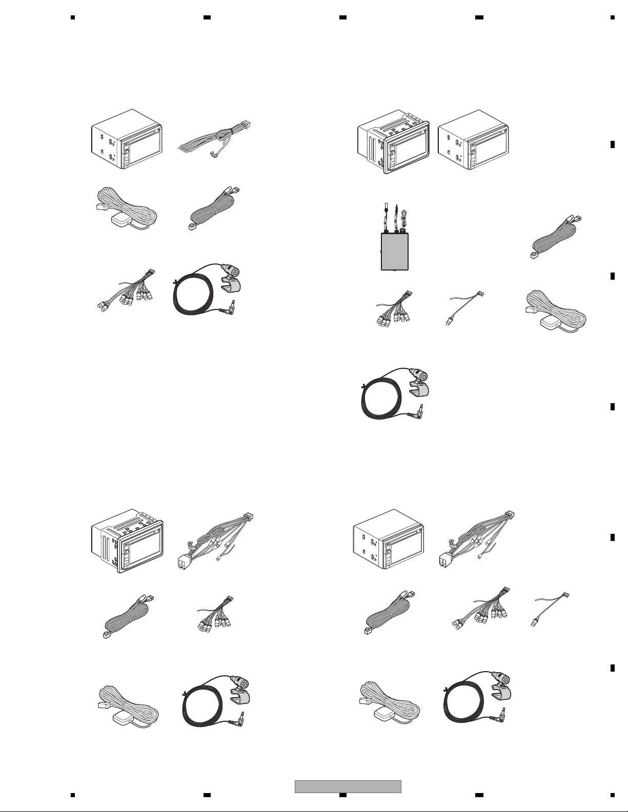
Parts supplied
AVIC-X940BT/XNUC
AVIC-X940BT/XNUW5
The navigation unit Power cord
CDP1479
GPS antenna
CXE3204
CXE3204
CXE3204
CXE3204
USB and mini-jack
CDP1425
CDP1425
CDP1425
CDP1425
connector
RCA connector
CDP1375
CDP1375
Microphone
CPM1083
CPM1083
CPM1083
CPM1083
AVIC-F940BT/XNEU5, AVIC-F840BT/XNEU5
(AVIC-F940BT/XNEU5) (AVIC-F840BT/XNEU5)
(AVIC-F940BT/XNEU5) (AVIC-F840BT/XNEU5)
The navigation unit
CDP1306
CDP1306
RDS-TMC tuner
CXE2176
USB and mini-jack
connector
RCA connector
CDP1376
CDP1376
CDP1460
CDP1460
GPS aerial
Microphone
The navigation unit Power cord
USB and mini-jack
connector
RCA connector
GPS aerial Microphone
AVIC-F940BT/XNAU, AVIC-F840BT/XNAU
(AVIC-F940BT/XNAU)
The navigation unit Power cord
USB and mini-jack
connector
RCA connector
GPS aerial Microphone
(AVIC-F840BT/XNAU)
RCA connector
The navigation unit
RCAconnector
AVIC-X940BT/XNUC
15
Page 16
1234
1234
C
D
F
A
B
E
2.2 DISC/CONTENT FORMAT
The Bluetooth word mark and logos are owned by the Bluetooth SIG, Inc.
and any use of such marks by Pioneer Corporation is under license.
Other trademarks and trade names are those of their respective owners.
16
AVIC-X940BT/XNUC
Page 17

5 678
56
7
8
C
D
F
A
B
E
To keep the product quality after servicing, please confirm following check points.
No. Procedures Item to be confirmed
1 Confirm whether the customer complain has
been solved.
If the customer complain occurs with the
specific media, use it for the operation
check.
The customer complain must not be
reappeared.
Display, video, audio and operations must
be normal.
2 DVD Measure playback error rates at the
innermost and outermost tracks by using the
test mode with the following disc.
DVD test disc (GGV1025)
Deterioration of mecha-drive can be
checked.
The error rate must be less than the
threshold value.
(Refer to the chapter of DIAGNOSIS for the
threshold value.)
3 DVD Play back a DVD.
(Menu operation; Title/chapter search)
Display, video, audio and operations must
be normal.
4 CD Play back a CD.
(Track search)
Display, audio and operations must be
normal.
5 FM/AM tuner Check FM/AM tuner action.
(Seek, Preset)
Switch band to check both FM and AM.
Display, audio and operations must be
normal.
6 GPS positioning Connect GPS antenna to the product, and
check whether the current location is correct.
Current location must be correct.
Display and operations must be normal.
7 Gyro action On "3D Calibration Status", check whether
the gyro sensor works well by moving the
front face of the product from left to right and
up and down.
Gyro-sensing, display and operations must
be normal.
8 Map display
Touch-panel
operation
Remote-control
operation
Check functions of map scale change and
map scroll.
Display and operations must be normal.
9 Delete data added during the operating
check.
Check whether no media (CD etc.) is inside
the product.
Make sure to delete data added during the
operating check.
The media used for the operating check
must be ejected.
10 Appearance check No scratches or dirt on its appearance after
receiving it for service.
See the table below for the items to be checked regarding video and audio:
Item to be checked regarding video Item to be checked regarding audio
Block-noise Distortion
Horizontal noise Noise
Dot noise Volume too low
Disturbed image (video jumpiness) Volume too high
Too dark Volume fluctuating
Too bright Sound interrupted
Mottled color
3. BASIC ITEMS FOR SERVICE
3.1 CHECK POINTS AFTER SERVICING
AVIC-X940BT/XNUC
17
Page 18
1234
1234
C
D
F
A
B
E
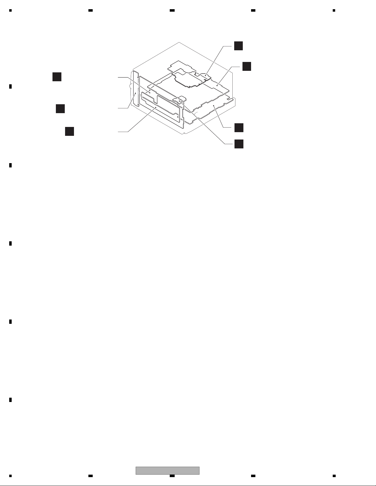
3.2 PCB LOCATIONS
AV Unit
A
CC Monitor Unit
(Service)
F
LCD-IF Unit
G
C
DVD Core Unit
D
IF PCB
Keyboard PCB
B
Micro SD PCB
E
A:AVIC-X940BT/XNUC
B:AVIC-F940BT/XNEU5
C:AVIC-F840BT/XNEU5
D:AVIC-F940BT/XNUW5
E:AVIC-F940BT/XNAU
F:AVIC-F840BT/XNAU
Unit Number : CWN6406(A)
: CWN6407(B)
: CWN6410(C)
: CWN6408(D)
: CWN6409(E)
: CWN6411(F)
Unit Name : AV Unit
IF Unit
Consists of
Keyboard PCB
IF PCB
Micro SD PCB
Unit Number : CWN6412(A)
: CWN6413(B)
: CWN6416(C)
: CWN6414(D)
: CWN6415(E)
: CWN6417(F)
Unit Name : IF Unit
Unit Number : YWX5033
Unit Name : DVD Core Unit
Unit Number : CXX4255(A)
: CXX4256(B)
: CXX4259(C)
: CXX4257(D)
: CXX4258(E)
: CXX4260(F)
Unit Name : CC Monitor Unit(Service)
Unit Number : CWN6419
Unit Name : LCD-IF Unit
18
AVIC-X940BT/XNUC
Page 19
5 678
56
7
8
C
D
F
A
B
E
Jigs List
RemarksJig No.Name
DISC GGV1025 Check points after servicing,
Inspection method of Pickup Unit
DISC TCD-782 Inspection method of Pickup Unit
20P FFC Extension Cable GGF1158 AV UNIT <---> IF PCB
50P FFC Extension Cable GGD1250 AV UNIT <---> IF PCB
30P FFC Extension Cable GGD1222 AV UNIT <---> DVD CORE UNIT
50P Extension Board GGF1656 IF PCB <---> CC MONITOR UNIT
50P FFC Extension Cable GGD1250 IF PCB <---> CC MONITOR UNIT
80P FPC Extension Cable GGD1633 AV UNIT <---> CC MONITOR UNIT
Test Mode File GGS1109 Test Mode
Grease List
DVD Mechanism ModuleGEM1024Grease
DVD Mechanism ModuleGEM1038Grease
DVD Mechanism ModuleGEM1045Grease
RemarksJig No.Name
3.3 JIGS LIST
Use the cable used in this product.
IF PCB
DVD Mechanism Module(LS2)
GGD1222
GGD1633
GGF1158
GGF1656
AV Unit
GGD1250
GGD1250
CC Monitor Unit (Service)
AVIC-X940BT/XNUC
19
Page 20

1234
1234
C
D
F
A
B
E
3.4 CLEANING
Before shipping out the product, be sure to clean the following portions by using the prescribed cleaning tools:
Portions to be cleaned Cleaning tools
DVD pickup lenses Cleaning liquid : GEM1004
Cleaning paper : GED-008
Portions to be cleaned Cleaning tools
Fans Cleaning paper : GED-008
20
AVIC-X940BT/XNUC
Page 21

5 678
56
7
8
C
D
F
A
B
E
AVIC-X940BT/XNUC
21
Page 22
1234
1234
C
D
F
A
B
E
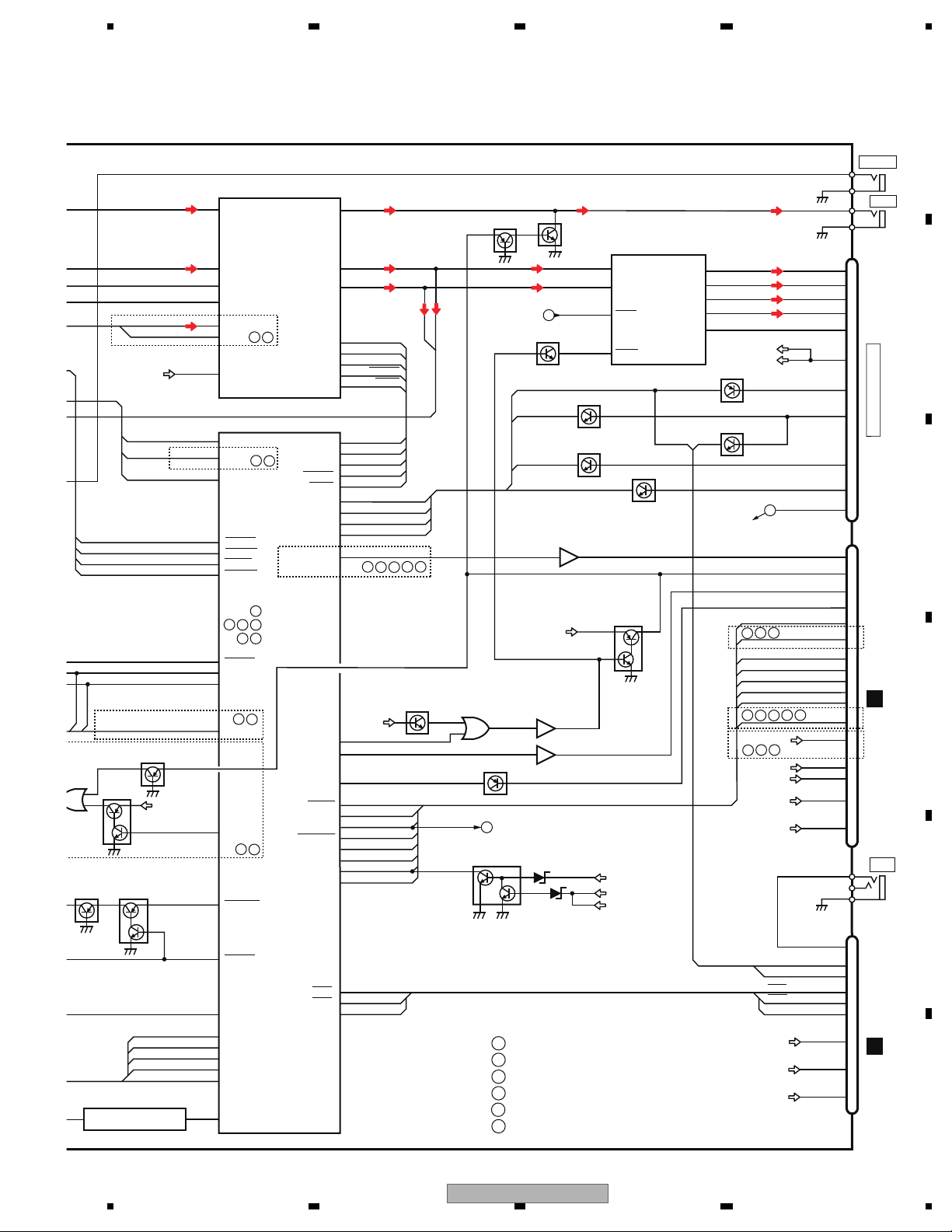
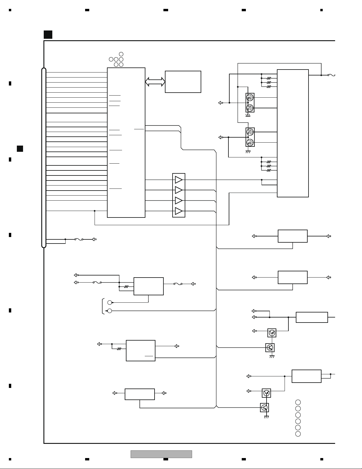
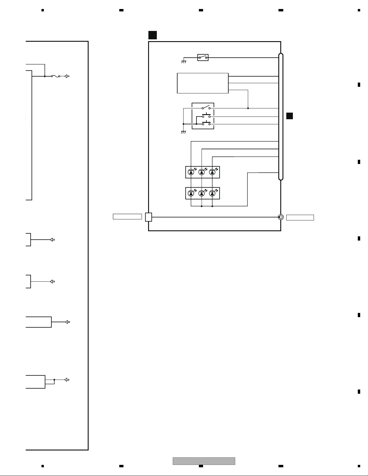
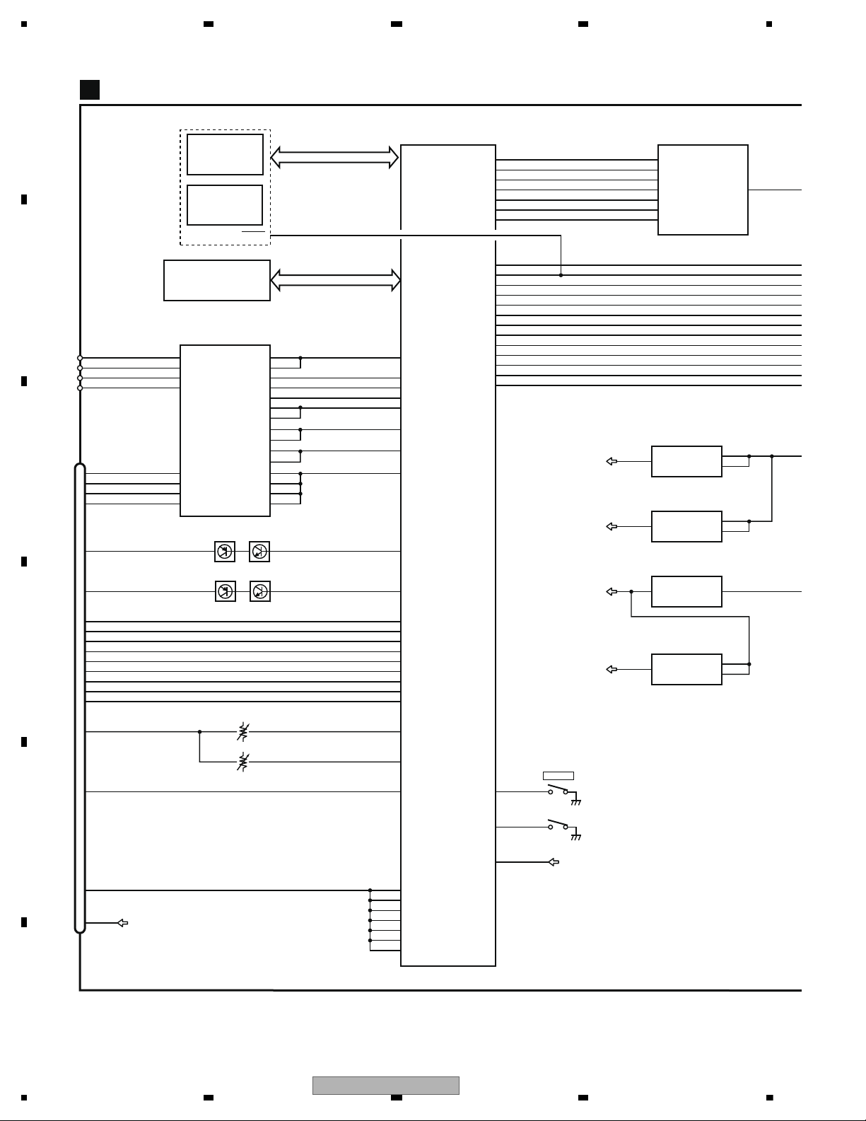
4. BLOCK DIAGRAM
Note: When ordering service parts, be sure to refer to " EXPLODED VIEWS AND PARTS LIST" or
"ELECTRICAL PARTS LIST".
JA1891
180
CN2301
1
20
CN1851
120
CN291
150
CN101
GPS
JA151
1
C
RCA TERM
CODE
AV(PREOU
B, D
A, E
A
115
CN3303
FFC
1
40
1
2
B
BT
MODULE
CDE9389
CN5607
CN5608
150
80
1
FPC
FPC
GPS ANTENNA ASSY
CXE3204
14
CN3360
CN3300
FPC
TOUCH PANEL
CSX1164
1
10
FPC
LCD PANEL
CWX4028
CN3201
118
JA4712
SD CARD
Connector
1
16
1
16
1
14
CN4602
CN5952
CN5951
FFC
MICRO SD CARD
CONNECTOR
TO
B
11 1
CN3302
1
11
FFC
CN2902
115
CN2902
2
1
2
1
FFC
CWX4254
CODE ASSY
1
CN5104
60
1
CN5004
60
110
FPC
101
FFC
1
CN5605
40
FFC
1
CN5001
40
CN5002
CN5102
1
110
10
CN5101
1
40
FPC
FPC
CN5103
CN5003
FFC
CN3200
1
10
CN2901
CN2901
C, F :
G
LCD-IF UNIT
E
MICRO SD PCB
IF UNIT
Consists of
KEYBOARD PCB
IF PCB
MICRO SD PCB
F
CC MONITOR UNIT(SERVICE)
BT/DISPLAY SECTION
7/7
F
VIDEO DEC/T-CON SECTION
6/7
F
NAND SECTION
5/7
F
DDR/FLASH_ROM/SRAM SECTION
4/7
F
CPU AROUND SECTION
3/7
F
CPU SECTION
2/7
F
P/S I/F SECTION
1/7
F
KEYBOARD
PCB
B
KEYBOARD
PCB
NM
NM
NM
NM
except C, F
4.1 OVERALL CONNECTION DIAGRAM
22
AVIC-X940BT/XNUC
Page 23
5 678
56
7
8
C
D
F
A
B
E
C
D
B
E
A
F
ASENBO
5
9
IPR+
IPLG
IPBUS-
IPL+
4
IPL-
11
IPR-
7
3
IPBUSG
8
10
IPRG
NC
1
2
IPBUS+
6
RR+
SPEED
PULSE
REVERSE
FR-
RL-
BREM
FR+
P.BREAK
RR- RL+
ILM
ACC
FL+
B.UP
FL-
GND
AVIC-F840BT/XNEU5
AVIC-F940BT/XNAU
AVIC-F940BT/XNUW5
AVIC-F940BT/XNEU5
AVIC-X940BT/XNUC
CN1521
30
1
1
30
CN1952
JA2351
MIC
IP-BUS
JA1001
FUSE
JA2061
JA1891
150
CN2401
101
CN2201
CN2301
1
20
CN1851
101
CN101
FFC
16
CN251
CXE2176
RDS-TMC TUNER
150
CN103
120
CN291
CN101
GPS
JA151
124
CN261
FAN
FAN MOTOR
CN201
21
Wired Remote
Jack
JA241
POWER SUPPLY TERMINALS
CODE ASSY
B, D, E, F: CDP1306
A : CDP1479
CN231
13
CN301
CANBUS
Connector
CDE9388
RCA TERMINAL
CODE ASSY
AV(PREOUT) TERMINALS
B, D : CDP1376
A, E : CDP1375
AV24
CODE ASSY
4PIN JACK
USB-A
JUNCTION SOCKET
17PIN PLUG
USB/iPod
CONNECTOR
USB EXT
CDP1425
1
17
FFC
FFC
FFC
GPS ANTENNA ASSY
MIC ASSY
CPM1083
JA1831
AVIC-F840BT/XNAU
C, F : CDP1460
C
DVD CORE UNIT
DRIVE UNIT
D
IF PCB
A
AV UNIT
FLAP SENSOR IF
5/5
A
TUNER/VICS SECTION
4/5
A
AUDIO SECTION
3/5
A
SYSTEM uCOM SECTION
2/5
A
PS/IF SECTION
1/5
A
except C, F
NM
only A, D
only B, C
only B, C
AVIC-X940BT/XNUC
23
Page 24
1234
1234
C
D
F
A
B
E
4.2 BLOCK DIAGRAM
JA2061
RFIN1
18
33
5
32
57
34
TDA7706
IC2001
RF FRONT END IC
FMMIXIN1
I2CSDA
RDSINT
31
RSTN
LNAIN
DACOUTL
I2CSCL
TUNPCK
TUNPDA
TUNRST
RDSINT
TUN_L_HIT
ANTENNA
RDS TMC TUNER
16
PINDIN
I
AV UNIT(1/2)
A
CN2301
74
MONO
80
AVSELOUT
75
GNDAZ
72
NAVI_L
22
AS_SDA0
20
AS_SCL0
68
PLL_ON
73
GNDN
25
GMUTE
62
TCON_SCL
64
TCON_SDA
71
69
13
CN1521
STANBY12LS1
→ SRX
11
S
→ LS1TX
10
IRQPWR9XRES
7
VDD5
19
COMPOSIT
SPEED_IN
24
23
PCHNG
18
SPEED
LS1VDD
1
VD(Dry)2VD(Dry)
3
VD8V
VD(Reg)
5
1
IC1471
NJM2904M
SPEED SENS
17
LOUT
LS1L
8
AMUTE
Q1472
Q1471
11
IPL-
8
ASENBO
7
IPL+
IP_LG
IP_L
1
IPBUS+
5
IPBUS-
JA1831
AU8
47
iPod_L
43
iPod_V
44
iPod_VG
46
iPod_AG
6
(BCV)
5
(BCVG)
CN2401
VTR2L
17
VTRIN2V
VTRIN2VG
VTR2V
VTR2VG
13
VTR2LG
MFL
3
4
5
6
RLOUT2
9
MRL
CN1851
IP-BUS DRIVER
IC1831
HA12241FP
ROUTBUS+
DIN1BUS-
62
8
1
5
STBY
Q1831
Q1832
BUP
ASENBO
22
REARLOUT
REARVOUT
LOUT2
45
SDA
17
RSTN
43
LIN1
11
VIN1
9
VIN2
8
VGND2
5
VIN4
4
VGND4
3
VIN5
2
VGND5
GND3
LIN4
40
39
LIN2
LIN3
36
35
33
GND4
32
GND2
46
SCL
IICSDA
IICSCL
AK4223VQ
IC1691
AV SELECTOR
24
LOUT1
14
VOUT1
13
VOUT2
LS1V
iPod_V
iPod_VG
BCV
BCVG
7
3
2
4
1
3
BA4558RFVM
GUIDE ISO/LPF
IC1641
NJM2125F
AU4.3 REG.
IC1621
AU84
RDSINT
TUNPCK
TUNPDA
TUNRST
IPTOS
STOIP
IPPW
Q1752
Q1522
Q1521
AU84
Q2442
AU84
iPod_L
iPod_AG
VTR2L
VTR2G
NAVI_L
GNDN
(1/2)
Q2441
IC1301
S-80929CNMC
2
POWER ON R
VDD33
15
14
5
ADS7828E
IC2223
ADC
GY2221
GYRO
SCL
16
+VDD
SDA
CH4
665
CH5
7
CH6
1
CH0
2
CH1
3
CH2
VREF
VOUT
VOUT
8
VDD
1
VDD
CSX1149
IC2222
G SENSOR
12
10
8
OUTX
OUTY
OUTZ
15
RES2
14
VDD
SN2221
TEMP
4
5
1
VDD5
VIN
VOUT
S-1167B30-M5
ON/OFF
3
IC2221
AD3 REG.
Q1664
Q1662
AU84
Q1861
Q1862
Q1866
Q1865
IP_LG
IP_L
TUN_
GUID
AV_L
iPod_
Q1751
IICSDA
IICSCL
(1/3)
CN103
D
CN291
D
CN5607
F
IP-BUS IN
CN1952
C
CCDIO3
56
VDD33
49
SWVDD33
VDD3
+
-
+
-
BCV
BCVG
REARLOUT
ASENBO
IICSCL
IICSDA
ASENB
CCD3_IOON
SENSOR
STAN
LS1
→
S →
IRQP
XRES
GND SELECT
GUIDE MUTE
Q17
DUAL ZONE
SENSOR
AEQ/AUX SW
B
C
A
D
E
F
A
D
D
E
A
B
A
B
D
E
24
AVIC-X940BT/XNUC
Page 25
5 678
56
7
8
C
D
F
A
B
E
ROT2
49
DETACH
27
ROT1
47
I
G
128
TC74VHCT541AFK
IC1511(1/3)
3V→5V
(2/2)
50
PREMUTE
11
(ANTON5)
7
FANON
18
TELMUTEIN
8
REMIN
48
RDSSNS
49
TMC_ON5
38
FANCONT
26
DDCLOCK
40
WREMIN2
41
WREMIN1
42
BSENS
9
10
13
14
17
|
SWVDD33
BUP
NKBUP
19
23
|
CCD5
CCDIO3
17
26
30
|
CCD5
40
43
|
CCD3
ILMV
BUP
Q1501
119
137
TC74VHCT541AFK
IC1511(2/3)
3V→5V
Q1191
MUTEBUP
Q1302
1
8
14
5
12
3
21
23
4SYSPW5
22
PA2030A
IC1051
POWER AMP
IN2
OUT2(+)
OUT2(-)
IN4
OUT4(+)
OUT4(-)
25
H-SW/VOS-DET
STBY
MUTE
JA1001
JA1891
8
9
12
5
7
6
RL+
RL-
PKB
PKB
BUP
FL+
FL-
16
BUP
NKBUP
13
STOIP
51
IPTOS
50
IPPW
70
XRES
64
IRQPW
82
SYSTOD
90
DTOSYS
88
LS1STBY
77
POWER SUPPLY
CN2401
BREM
60
Rear_L
59
Pre_SWL
31
DATA
14
IN5L
18
Mic_in
8
IN2L
9
IN3L
12
IN4L-
11
IN4L+
32
STB
PML020A
IC1761
E-VOL
61
Front_L
30
CLK
28
SACLK
27
SA_TEST
VDT
VST
VCK
54
VP
AU84
REARVOUT
SYSTEM u-COM
IC1302 (1/2)
Q1031
11
REVSYSREV
Q1012
Q1011
ILM
SPEED
ACC
ILMSNS Q1141
14
10
ASENS
Q1151
LCH
VIDEO
RDSINT
9
RDSINT
TUNPCK
6
TUNSCL
TUNPDA
5
IICSDA
1
TUNSDA
TUNRST
107
TUNRST
144
IICSCL
98
RMUTE
127
MICSENL
36
AV_RST
VDT
VST
VCK
SPECLK
SPEIN
96
95
97
92
99
PBSENS
BKSNS
ILMSNS
ASENS
72
89
52
103
MUTE
30
ANTON
81
TELMUTE
68
Q1752
MUTEBUP
Q1793
PREMUTE
SW OUT MUTE
Q1181
TO 2/2
MFL
MRL
84
TMC_MSN_ON
131
GNDSEL
75
DDCLK
ASENBO
FANCONT
WREMIN2
37
FANON
112
71
105
136
WREMIN1
REMIN
RDSSNS
137
4
BSENS
104
119
RESET
19
IC1301
S-80929CNMC-G8Z
21
POWER ON RESET
45
PKB
MIC+
REV
9
11
13
ROT_IN2
DETACH
ROT_IN1
CN2301
(2/3)
JA2351
MIC
Q1861
Q1862
26
AEQSW
IP_LG
IP_L
TUN_L
GUIDER
AV_LOUT1
iPod_L
PKB
SYSREV
IICSDA
IICSCL
FL
RL
H
PREMUTE
TO 2/2
DDCLK
BUP
BUP
Q1131
CN5607
F
CN103
D
ASENBO
SPECLK
SPEIN
STANBY
LS1
→ SRX
S
→ LS1TX
IRQPWR
XRES
Q1753
DUAL ZONE
VIDEO
VGND
SWL
SWL
LGND
AMP MUTE
GNDD
MIC
PKB
REV
ILMSENS
ASENS
REVPKB
PREMUTE
OFFMUTE
BSENS
NKBUP
DDCLK
Q1801
REV
ROT2
ROT1
AEQ/AUX SW
:AVIC-X940BT/XNUC
:AVIC-F940BT/XNEU5
:AVIC-F840BT/XNEU5
:AVIC-F940BT/XNUW5
:AVIC-F940BT/XNAU
:AVIC-F840BT/XNAU
A
B
C
D
E
F
D
E
F
D
E
F
A
B
C
E
F
A
D
A
D
A
B
C
E
F
A
D
A
E
E
PEQ006A8
PEQ004A8
PEQ005A8
F
A
B
C
D
AVIC-X940BT/XNUC
25
Page 26
1234
1234
C
D
F
A
B
E
AV UNIT (2/2)
A
PWRBL
47
PWRBL
48
DDCLK2
35
ILMOSC(DDCLK2)
16
IC1111
BD3931FP
1
3
VDD5
MUTEBUP
Q1122
Q1121
VDD5 REG.
SWVDD5
1
3
5
VDD33
ON/OFF
VOUT
VIN
VDD33 REG.
IC1091
S-1200B33-M5
1
2
VD8V
SW
VIN
BD9781HFP
EN
7
DDCLK
BU
1
4
2
ACC84 REG.
IC1161
NJM2388F84
ACC84
CONTROL
VOUT
VIN
IC1241
MOT8 REG.
G
TO 1/2
H
CCD5
22
SW1
SENSE1+
TG2
SW2
SENSE2-
TG1
BG1
CONVERTER
IC1201
LTC3850IGN
VIN
CCD3
26
2
VFB1
6
SENSE1-
3
25
23
11
RUN1
1
RUN2
13
MODE/PLLIN
27
16
SENSE2+
12
VFB2
8
17
20
BG2
Q1204
Q1205
P1201
P1243
BUP
P1242
ILMV
BU
NKBUP
1
4
2
AU84 REG.
IC1171
NJM2388F84
AU84
LS1VDD
CONTROL
VOUT
VIN
LS1VDD REG.
IC1281
LT3505EDD
SW
VIN
2
FB
7
SHDN
4
Q1102
Q1101
SWVDD33
(3/3)
IC1511
TC74VHCT541AFK
182
173
164
155
3V→5V
NAVION
48
ACCPW
114
SWACPW
67
SYSPW
69
NAVION5
ACC84
2
1
4
TU5V REG.
IC1941
NJM2846DL3-05
TU5V
CONT
VOUT
VIN
SYSTEM u-COM
IC1302 (2/2)
125
TUON1
TUON1
60
VD5CONT
VD5CONT
ACCPW5
SWACPW5
SYSPW5
ACCPW5
SYSPW5
VD5CONT
SYSPW5SYSPW5
ACCPW5
TUON1
SWACPW5
CN2301(3/3)
3
P1291
BUP
CN5607
F
DC/DC
SWVDD5 REG.
SWVDD33 REG.
6
5
INV
FB
66
PIPRST
3
KDT0
6
5
FCONT_C
KDT1
7
KDT2
55
4
CASHFSNS
MOVITEMP
PIPRST
113
KDT0
138
FCONT_C
126
KDT1
139
KDT2
133
CARDSNS
73
CCTEMPIN
129
CTOSYS
116
44
CTOSYS
65
LCDTEMP
77
DIMMER
63
MBLPW
LCDTEMPIN
134
108
DIMMER
80
MBLPW
SYSTOC
118
BLSYNC
33
NAVION2
111
76
NAVION2
46
SYSTOC
BLSYNC
61
OFFOK
66
ILMRST
54
OFFOK
60
BSENRQ
63BSENRQ
67
10
ILMRST
14
COMDC
57
ILMSDA
12
ILMCK
COMDC
3
BLERR2
59
BLERR2
100
CPUWDT
58
CPUWDT
61
40
ILMSDA
38
ILMSCL
21
RDSSNSO
128
RDSSNSO
ASENRQ
55
56
CCRST
51
50
ASENRQ
NAVIRST
EEPROM
IC1303
S-93C56BD0I-I8
:AVIC-X940BT
:AVIC-F940BT
:AVIC-F840BT
:AVIC-F940BT
:AVIC-F940BT
:AVIC-F840BT
A
B
C
D
E
F
E
PEQ006A8
PEQ004A8
PEQ005A8
F
A
B
C
D
26
AVIC-X940BT/XNUC
Page 27
5 678
56
7
8
C
D
F
A
B
E
IC1111
1
1
3
ON/OFF
VIN
BUP
1
22
P1201
NKBUP
BUP
1
.
NKBUP
VDD5
BT ANTENNA
RG
54
1
2
3
B
JA2901
12
RGB
1
D2902
D2901
CN2902
4
3
5
6
7
KEY MATRIX
VOLUME/POWER OFF
DETACH
ILMB1
1
ILMV
KEY2
DETACH
KEY1
2
KEY0
14
ROT_IN1
13
ROT_IN2
ILMR1
ILMG1
KEYBOARD PCB
B
S3004, S3005, S3006,
S3007, S3008
CN2901
1
S3001
S3003
CN3303
F
BT MODULE
AVIC-X940BT/XNUC
27
Page 28
1234
1234
C
D
F
A
B
E
RESET
12
VCC5
VD8
PU (DP11)
SDRAM
IC1480
M12L64164A-5TG2M
24
17
VO4+WHITE
14
VO2+
MOTOR DRIVER
IC1251
BA5839FP
OPINSL
23
OPOUTSL
27
OPIN3+
7
OPOUT1
2
OPIN2+
5
OPIN1+
22
LDIN
21
CNT
9
MUTE
151
SYSTEM uCOM
IC1501
MN2DS0018MA
ADOUT
150
LRCK
VCC5
1
T+
12
VO1+
2
F-
11
VO1-
3
F+
13
VO2-
4
T-
6
TEMP
10
F+H/G+H
16
B
17
A
18
C
19
D
20
FE1
21
FE2
11
E+G/E+F
13
78LD
14
65LD
9
VCC
CN1101
DVD CORE UNIT
C
VR1101
FLASH ROM (16M x 2)
IC1401
CWW5043
IC1402
CWW5044
LECRGM
18
VO4-GREEN
LECRGP
15
VO3+BLK
SPDLM
16
VO3-
7
ADAC
IC1801
PCM1753DBQ
VCC5 REG.
IC1002
VOUT
VIN
5
4
ON/OFF
3
S-1133B50-U5
VCC5_AU
VCC5-AU REG.
IC1003
VOUT
VIN
5
1
ON/OFF
3
S-1200B50-M5
VCC33
VCC33 REG.
IC1004
Vout
Vin
3
1
NJM2855DL1-33
VCC12
VCC12 REG.
IC1953
VOUT
VIN
1
6
ON/OFF
4
S-1135D12-A6
VOUTL
2
DATA
3
LRCK
149
SRCK
1
BCK
148
DACCK
16
SCK
57
SDODAC
13
MD
58
SCKDAC
14
MC
56
LTDAC
75
EXTRG1
70
NRES
48
IRQPWR
53
CMDCOMN
54
STSCOMN
191
STANDBY
138
COMPOSITE
144
LOUT
146
ROUT
152
IECOUT
47
I2C_SCL
46
I2C_SDA
65
HOME
61
CP_Reset
15
ML
RED
SPDLP
67
CRGDRV
62
LDIN
63
CONT1
64
CONT2
6
OPIN1-
127
FD
4
OPOUT2
126
TD
25
OPOUT3
66
MD
1
VR
110
VHALF
122
TEMP
112
F+H_G+H
100
VIN3RF
99
VIN4RF
98
VIN2RF
97
VIN1RF
115
VIN7
116
VIN8
23
RF
96
RFINP
8
Vref
109
VREFH
113
VIN5
114
VIN6
117
VIN3
118
VIN4
119
VIN2
120
VIN1
22
IMON
105
CDMPD
VR1102
103
DVDMPD
111
E+G_E+F
106
LPCO2
104
LPCO1
Q1102
S1
55
12EJ
121
VDSENS
S3
Q1104
Q1101Q1103
HOME
3
OPIN2-
26
OPIN3-
28
AVIC-X940BT/XNUC
Page 29
5 678
56
7
8
C
D
F
A
B
E
CN1521
A
ANALOG LOUT
14
AMUTE
23
XRESET
22
30
29
28
IRQPWR
21
HSTCMD
20
SLVSTS
19
STANBY
18
COMPOSITE
12
D-
9
D+
8
IECOUT
6
SCL
4
SDA
3
RESET
VD8
24
VD5
2
CN1952
7
4
3
1
3
1
6
4
VD8
AVIC-X940BT/XNUC
29
Page 30

1234
1234
C
D
F
A
B
E
IC223
TC7SET08FUS1
IC221
TC7SET04FUS1
2
1
4
24
WREMIN2
WREMIN1
TUNDI
TUNCS(TS_EN)
TUNDO(TS_DAT)
19
17
21
20
TUNCLK(TS_CLK)
OPEN
43
GRF_RESET
44
SHORT
42
GPS
GRF3I-0336S
IC151
IC195
TC7SH08FUS1
1,2 4
1
3
4
CCD5
TUNDO(VICSTOC)
TUNCS
TUNDI(CTOVICS)
TUNCLK
47
49
50
48
15
14
SPI_CLK
16
SPI_DO/MAG
SPI_DI
13
SPI_CEB
41
40
39
X_UTXD_1
X_USCLK_1
X_UTFS_1
GRFRST
19
GPS_MAG
IC191
TC7SH08FUS1
1,2 417
SIGN_MAG
GPS_SGN
IC187
TC7SH08FUS1
1,2 418
ACQCLK
5
RFIN
GPS_CLK
GPS_SAMPLE_CLK
50
GPS33 REG.
BU33TA2WNVX
IC153
VOUT
VIN
STBY
7
IO3
Q151
ANTIN
JA151
1
GPS ANTENNA
BA10358F
12
6
GPS_MAG
GPS_SGN
GPS_CLK
IF PCB
CN291
13
3
CN5608
FL
RL
RLOUT2
VTRIN2VG
VTRIN2V
VTR2LG
VTR2L
17
42
SWVDD33(VTR3V)
REMIN(VTR3VG)
43
6
9
5
4
CN103
CN101
1
45
33
25
46
PREMUTE
9
(BCV)
(BCVG)
TELMUTEIN
BSENS
7
4
8
5
13
iPod_V
11
10
44
iPod_VG
iPod_L
5
iPod_AG
34
22
23
33
KMODE
CTOEX
HYOKA
EXTOC
38
PPW
37
PVSNS
30
USB+
29
USB-
FANCONT
FANON
CN2401
CN1851
A
A
D
F
Q262Q261
49
48
46
IC381
BD9008F
8
5
VIN
EN/SYNC
2
4
3
SW
INV
FB
USB5 REG.
IC382
BD82001FVJ
2
3
IN1
IN2
4
EN
5
OC
6
8
7
OUT1
OUT3
OUT2
NKBUP
34
|
37
DDCLK
P201
BUP
IO3
DTV3
41
BUP
38
CCD5
28
|
32
IC152
IC101
RS-470
4
2
OUT
VCC
NKBUP
IN1-
OUT2
OUT1
IN2-
IR REMOTE
USB5
Q264
F151
5
IN2+
3
IN1+
CCDIO3
CANTOC
CTOCAN
CCD5
2
TMC_ON5
3
RDSSNS
CANTOC(ETCTOC)
CTOCAN(CTOETC)
25
26
35
CTOVICS(TMC/VICS common)
36
VICSTOC(TMC/VICS common)
PRE MUTE
1
PVIN
GPS33
A
BDE
DEF
30
AVIC-X940BT/XNUC
Page 31

5 678
56
7
8
C
D
F
A
B
E
CN231
JA241
2
4
USB+
USB-
A_RETURN
LOUT
V_RETURN
VOUT
USB 5V
1
7
11
12
13
1
3
2
WREMIN2
WREMIN1
USB/iPod
WIRED
REMOTE
CN261
CN201
14
2
15
3
7
9
22
10
23
5
PFL
PRL
RLOUT2
VTRIN2VG
VTRIN2V
TELMUTE
BCVG
BCV
12
11
21
(HYOKA)
24
EXTOC
CTOEX
KMODE
VTR2LG
VTR2L
Q263
P201
BUP
FAN REG.
2
FAN MOTOR
Q201, Q202
Q204, Q205
FANCONT
FANON
AV(PREOUT)
USB5
HYOKA
KMODE
FANV
GNDD
CN251
1
VICSTOC
CTOVICS
RDSSNS
TMC_MSN_ON
SWBUP
4
5
3
2
TPD1018F
IC252
SW BUP
TC7WH126FK
IC251
6
1
IN OUT
2
3
1
7
6
5
CANTOC
CTOCAN
CN301
CCD5
1
IC301
TC7SET08FUS1
2
1
IO3
IC303
TC7SH08FUS1
1
2
NTOCAN
2
CANTON
4
4
CANBUS
RDS-TMC TUNER
:AVIC-X940BT/XNUC
:AVIC-F940BT/XNEU5
:AVIC-F840BT/XNEU5
:AVIC-F940BT/XNUW5
:AVIC-F940BT/XNAU
:AVIC-F840BT/XNAU
A
B
C
D
E
F
B
C
A
BCE
F
A
AVIC-X940BT/XNUC
31
Page 32

1234
1234
C
D
F
A
B
E
CC MONITOR UNIT(SERVICE)(1/2)
CPLD
PE9019A
IC4621
17
I/O_16
I/O_22
I/O_80
I/O_18
I/O_17
I/O_15
99
19
18
16
AA18
AA22
Y22
AC22
X_VIP_PXD[13]
X_CKO_0
27 AC13
X_SPI_EN_1
X_SPI_CLK_1
X_SPI_DIN_1
A2
AC4
AA4
AB4
X_GPS_MAG
X_GPS_SGN
B3
X_UTXD_1
X_UTFS_1
AC16
B2
X_VIP_PXD[15]
X_GPS_CLK
W23
Y23
X_FA[24]
X_FA[25]
X_USCLK_1
A1
X_SAMPLE_CLK
VIDEO DECODER
IC5513
AK8859VN
X_VIP_PXD[10]
X_VIP_PXCLK
X_VIP_HSYNC
X_VIP_VSYNC
X_VIP_DVALID_FID
AC17
AC19
AC18
Y18
3
16
15
14
DTCLK
PDN
AB17
30
VD_F
VAR
HD
27
SDA
AIN1
X_SDA12
SCL
X_SCL11
X_VIP_PXD[0-7]
VIDEO PROCESSING IC
IC4901
TC90192XBG
X_L_FCK
X_L_LCK
X_L_PCLK
F2
F1
E1
R4
T4
U4
45_D-RGB_H_IN
58_D-RGB_Clk_IN
N1
36_D-YUV_Clk_IN
M1
33_OSD_B4_H_IN
M2
34_OSD_B5_V_IN
46_D-RGB_V_IN
U16
98_DAC_OUT
U15
94_PLL_IN
P17
145_STV1
106_C.Video_IN1
C16
153_Load
E17
154_STH
160_CPH
C17
B17
147_CPV
E16
140_Vcom1
F17
LDD_R[1-5]
D
55_I2C_Clk_IN
56_I2C_Data_IN
U3
U2
49_Reset_IN
T1
AC97CODEC
WM1616LGEFL
IC4654
X_VIP_PXD[11]
X_AC97_SYNC
X_AC97_DIN
X_AC97_BIT_CLK
X_AC97_DOUT
W2
Y2
W1
Y1
10
8
6
5
SYNC
RESETB
AB16
X_VIP_PXD[12]
Y16
X_SD_VCC_ON_1
T5
11
BITCLK
SDATAOUT
SDATAIN
LINEL
MONO
HPL
31
39
23
LINE_L
X_TXD_2
AB3
CTOS
X_GPIO[5]
AC14
W10
XCCSTBY
CC_RST
X_YN
X_YP
H23
H22
SDA_1
SCL_1
X_SCL1
X_SDA1
D1
D2
nRESET
X_VIP_PXD[9]
Y19
I2C_SDA/SPI_SOMI
13
I2C_SCL/SPI_SIMO
12
4
iPod AUTHENTICATRION IC
IC4701
341S2162
SD3CCD3
IC4212
IC4207
TC7SH08FUS1
TC7SH08FUS1
2
1
4
X_RESET_B
2
1
4
CCD5
IC4203
S-80944
POWER ON RESET
CCD3
POWER ON RESET
IC4206
S-80929
SN
CPU
TT4421
IC4001
2
1
2
1
CN101
CN2301
JTG_RST
JTG_RST
Q4903
X_XN
F23
Q4701
eNAND TE
LDD_G[0-5]
LDD_B[1-5]
CN5608
39
41
48
46
40
49
X_UTFS_1
44
X_UTXD_1
43
X_USCLK_1
42
GPS_MAG
50
GPS_SGN
GPS_CLK
GRF_RESET
OPEN
SHORT
GPS_SAMPLE_CLK
AA23
K1
N5
P5
X_IDE_DACK_B
X_TXD_1
W3
X_SD_CD_B_0
X_SD_VCC_ON_0
AB15
Y3
X_UTXD_2
X_RXD_1
AC5
W15
X_USB_DP
X_URXD_2
X_LDD[20]
AB5
X_USB_DN
38
37
34
33
23
22
PPW
35
PVSENS
36
KMODE
30
HYOKA
29
CTOEX
EXTOC
CTOVICS
VICSTOC
USB+
USB-
X_RXD_0
AA1
26
CANTOC/ETCTOC
X_TXD_0
AB1
25
CTOCAN/CTOETC
X_VIP_PXD[0-7]
TOP
BOTTOM
L
G
CTOSYS
OFFOK
NAVIRST
37
21
31
CN5607
(1/4)
24
AK
IC
5
11
RST
AOU
3
1
2
NJM2746RB1
IC5451
-
+
BT_RES
X_UTXD_0
AC2 CTOBT
X_URXD_0
AA2 BTTOC
X_IDE_IRQ
W16 BT_BOOTS
Q3360
D
F
A
LCD_D25
D
D
Q4206
Q4209
(1/2)
SD3 REG.
CN4602
SD3
SD_DATA[0] - SD_DATA[3]
10
.
.
.
3
13
15
5
VDD
SD_DET
SD_CL
SD_CMD
U1
X_SD_CMD_1
V1
X_SD_CLK_1
U5
X_SD_CD_B_1
1
7
11
CN5952
E
CNMC-G9E
CNMC-G8Z
X_SCL1
X_SDA1
Y19
(1/2)
32
AVIC-X940BT/XNUC
Page 33

5 678
56
7
8
C
D
F
A
B
E
IC4406
CY62147EV30LL45BVA
IC4403
CXX4262
27
X_SDA12
X_SCL11
P17
C16
E17
C17
B17
STH1
DCLK
39
STV1
13
E16
F17
CPV
12
VCOM1(POL)
11
14
FCONT_C
9
NAVION2
16
COMDC
24
NAVION2
5
D_R[0-5]
U3
U2
T1
TCON_SDA
TCON_SCL
PIPRST
NAVI_L
MONO
13
12
MOVITEMP
AVSELOUT
1
19
17
15
9
7
I2S_OUT1
VCC
38
I2S_MCLK
37
23
24
I2S_CLK
35
I2S_SYNC
39
NRESET
10
77
18
23
J2
X_LDD[16]
J1
X_LDD[17]
J3
X_LDD[18]
K2
X_LDD[19]
C2
X_GPIO[1]
AC3
X_RXD_2
E22
X_SDA_0
AB14
X_GPIO[6]
AA14
X_GPIO[7]
E23
X_SCL_0
23
36
63
56
30
GMUTE
PCHNG
ASENRQ
35
CPUWDT
59
61
14
SYSTOC
AD_SDA0
AD_SCL0
73
REV
PKB
BSENRQ
L1
X_LDD[22]
60
RDMSDSENS
74
KDT2
76
KDT1
78
KDT0
68
DETACH
70
ROT_IN2
72
ROT_IN1
67
ILMSCL
69
ILMSDA
71
4
ILMRST
CN2301
CN2301
SN4201
CN5605
CN5607
CPU
TT4421
4
eNAND TEMP. SENSOR
IC4401
H5DU5162ETR-E3C
IC4402
H5DU5162ETR-E3C
IC4404
H5DU5162ETR-E3C
IC4405
H5DU5162ETR-E3C
DDR SDRAM(512Mbit x 4)
SRAM(4Mbit)
FLASH ROM(8Mbit)
14
6
G
IC4407
TC7PA53FU
B5
CE
B4
RESET
K22
X_FCE_B[1]
|
5
8
4
|
25
30
|
32
37
|
CN5607
(2/4)
4
3
1
CN3300
TOP
BOTTOM
L
SPEED_IN
57
CN3360
24bit-DAC
AK4388VT
IC3360
5
11
RSTN
AOUTL
LRCK
4
MCLK
SDTI
1
3
BICK
2
BT_RESET
U0_IN
29
U0_OUT
30
BOOTS
9
9
10
ILMV
KDT2
KDT1
KDT0
512
11
10
4
IC3300
NJU6062V
RGB ILM DRIVER
3
LED1
LED2
LED3
SCL
SDA
RSTb
65
ILMOSC7
OSC
10
21
IC3200
OZ527IRN
LCD
9
OVP
ISEN1
8
ISEN2
7
ISEN3
5
ISEN4
VIN
16
SW
15
PREC
2
ENA
14
PWM
13
STATUS
ILMR1
ILMG1
ILMB1
3
2
4
11
13
12
14
15
KEY2
KEY1
KEY0
CN3303
ROT_IN1
ROT_IN2
DETACH
LCDTEMP
TH3201
(3/4)
BT MODULE TOUCH PANEL
A
A
8
10
6
5
4
3
K2
K3
K4
Anode
K1
CN3201
18
SYNC
20
BLSYNC
22
BLERR2
18
DIMMER
16
MBLPW
PWRBL
CCD3
CCD3_IOON
D_G[0-5]
D_B[0-5]
CN2902
B
IC4001(2/2)
VCC
LOAD
TEMP. SENSOR
BACKLIGHT DRIVER
IC4501
PEM002C8
moviNAND(4GByte)
|
CN5002
G
CN5001
G
4
3
1
CN3300
TOP
BOTTOM
L
TOUCH PANEL
B
FCONT_C
75
COMDC
10
:AVIC-X940BT/XNUC
:AVIC-F940BT/XNEU5
:AVIC-F840BT/XNEU5
:AVIC-F940BT/XNUW5
:AVIC-F940BT/XNAU
:AVIC-F840BT/XNAU
A
B
C
D
E
F
19
HSB
A
B
CEF
MIC1P
MIC+
80
5
AVIC-X940BT/XNUC
33
Page 34

1234
1234
C
D
F
A
B
E
CCD5
IO_ON
13
6
PLL_ON
CCD25
CCD25_PLLON
CCD5
P4202
IC4204
LTC3412AEFE
CCD25 REG.
10
11
14
SW_1
SW_2
SW_3
15
1
16
9
7
SW_4
SVIN
PVIN_2
PVIN_1
RUN/SS
OUTB
OUTA
VDDA
VDDB
CTRL
Q4207
Q4218
POWER ON RESET
IC4217
1
2
CCD5
4
IC4208
CCD3
LCD15
CCD5
4
IC4209
LCD25
NJM2878F3-15
NJM2878F3-25
CP3
Q4210
Q4211
4
5
1
IC4211
NJM2878F3-18
CCD3
VD18
CP18
IC4281
POWER ON RESET
1
2
PWRBL
CCD3
38
32
|
41
51
|
55
64
VDD3
25
CCD3_IOON
58
IC5514
NJM2125F
CC5
CCA25
CCA25 REG.
CP3 REG.
5
1
5
1
LCD15 REG.
LCD25 REG.
4
IC4361
NAND3
NJM2888F33
5
1
NAND3 REG.
VD18 REG.
CCD25_PLLON REG.
7
8
1
2
IC4219
BD6522F
CCD3
CCD3_IOON
CCA3_IOON
USB3
USB3 REG.
CCD3_IOON REG.
CC5
RTC33
BUP3
ILMV
CCD5
CCD3
SWAC33
CC3
4
CCD3
CCD12
PLL12
CCD5
P4201
CCD12 REG.
IC4205
LTC3412AEFE
10
11
14
SW_1
SW_2
SW_3
15
1
16
9
7
SW_4
SVIN
PVIN_2
PVIN_1
RUN/SS
PLL12 REG.
POWER ON RESET
IC4216
1
2
CCD5
Q4212
Q4214
Q4216
Q4217
VIN
VOUT
CONTROL
VOUT
VIN
CONT
VOUT
VIN
CONT
VIN
VOUT
CONT
CC MONITOR UNIT(SERVICE)(2/2)
F
CN5607 (4/4)
CCD5
CN2301
A
33
34
GNDA
8
GNDA
10
GNDA
12
GNDA
1
3
4
-
+
VDD3
PLL_ON
S-80844
CLMC-B65
S-80830
CLMC-B6P
S-80835
CLMC-B6U
LCD_D25
4
VFB
4
VFB
:AVIC-X940BT/XNUC
:AVIC-F940BT/XNEU5
:AVIC-F840BT/XNEU5
:AVIC-F940BT/XNUW5
:AVIC-F940BT/XNAU
:AVIC-F840BT/XNAU
A
B
C
D
E
F
AVIC-X940BT/XNUC
34
Page 35

5 678
56
7
8
C
D
F
A
B
E
CN2301
CN5952
9
5
3
CN5951
MICRO SD CARD
16
SD_DET
6
SD_CMD
10
SD_CL
4
7
VDD
SD_DET
SD_CMD
SD_CL
VDD
MICRO SD PCB
E
CN4602
F
SD_DATA[0] - SD_DATA[3]
8
7
2
1
.
.
.
14
12
4
2
.
.
.
AVIC-X940BT/XNUC
35
Page 36

1234
1234
C
D
F
A
B
E
LCD-IF UNIT
G
CN5605
F
CN3201
F
12
LOAD
COMDC
18
4
|
23
25
|
30
32
|
37
10
CN5001
5
8
VCC
|
R[0 - 5]
G[0 - 5]
B[0 - 5]
3
1
2
BA4558RFVM
IC5002
+
-
VCOM1
11
CPV
VSY
13
HSY
14
NAVION2
16
DCLK
39
IC5001
R1290K103A
STEP-UP DC/DC CONVERTER
6
4
CE
VIN
23
20
24
LX1
CPVCC
LX2
22
CPPSW
21
CPP
17
CPPFB
19
CPN
15
CPNFB
10
DTC
5
VREF
V34
Q5001
STEP-UP
VOLTAGE
STEP-UP
VOLTAGE
V18
V92
VM6
GRADATION
VOLTAGE
V92
V34
VM6
V18
V
8
10
6
5
4
3
K2
K3
K4
Anode
K1
|
CCN5002
V34
VR[1
7
VFB
36
AVIC-X940BT/XNUC
Page 37

5 678
56
7
8
C
D
F
A
B
E
CN5004
30
|
35
36
|
41
42
|
47
29
1
2
Vcom
LOAD
11
POL
14
VCLK
17
STV2
59
DIO1
23
HCLK
VOLTAGE
48
|
57
26
27
V92
22V34
8VM6
6V18
AVDD
DVDD
VEEG-6V
VDDG+18V
K2
K3
K4
Anode
K1
1
3
5
6
7
8
|
CN5003
LCD MODULE
LCD
LCD BACKLIGHT
XON(Hi)
10
L/R(Hi)
28
VR[1-10]
AVIC-X940BT/XNUC
37
Page 38

1234
1234
C
D
F
A
B
E
4.3 POWER SUPPLY SYSTEM FIGURE
A
+B
AV UNIT
System u-com
R5F64165DFD
RESET IC
S-80929CNMC
EEPROM
S-93C56BD0I-I8
SPEED I/F
NJM2904M
3 5 LEVEL SHIFT
TC74VHCT541AFST
ACCPW5
(syscom)
LC-Filter
UVDD33
TO IF PCB
SWACPW5
(syscom)
TELMUTE
Circuit
LSA1576UB
SWVDD5
LSA1576UB
SWVDD33
LSA1576UB
VDD5(Reg)
Constant
PowerSupply5V
BD3931FP
VDD33(Reg)
Constant
PowerSupply3.3V
S-1200B33-M5
ASENBO
(syscom)
IP-BUS POWER SUPPLY
SW
LSA1576UB
IP-BUS Driver
HA12241FP
IP-BUS
MAX:8.5mA
2mA
10mA
(150mA/0.3W)
100mA/0.17W
0.5A/1.6W
0.11A/1.045W
2mAMAX 45mA
TYP 32mA
47mA
2mA
HOLD BUP
4700[uF]/16[V]
CCD5/CCD3
LTC3850IGN
5.21V : Max1.6A
3.43V : Max1.36A
FET(7A)
TO CC MONITOR
UNIT(SERVICE)
1500mA
100mA
NAVION5
DDCLK2
(syscom)
TO IF PCB
1360mA
TO CC MONITOR
UNIT(SERVICE)
TO CC MONITOR
UNIT(SERVICE)
21mA
PK
LSA
PLLON
(prima)
GYRO Sensor
CSX1147XV8100CB
G Sensor
CSX1149LIS344ALH
ADC
ADS7828E
Temp S
S-58LM
3.0V(2.4V-3.6V)
TYP:0.68mA
MAX:0.85mA
3.0V
(2.7V-3.6V)
TYP:0.225mA
MAX:0.32mA
3.0V(2.
TYP:0.
MAX:0
3.0V±0.15V
TYP:1.7mA
MAX:2.7mA
: POWER SUPPLY
CCD5
CCD3
IPPW
(syscom)
P1291
SOC 1A
CEK1254-A
PWRBL
UC/UW5 Only
NKBUP
BUPV
P1201
SOC 3.15A
CEK1259-A
6.1inch :
max415mA
NKBUP
TO IF PCB
AD3V(Reg)
S-1167B30-M5TRB
AV UNIT
38
AVIC-X940BT/XNUC
Page 39

5 678
56
7
8
C
D
F
A
B
E
CE)
TO IF PCB
TO CC MONITOR
UNIT(SERVICE)
CCDIO3
PKB Circuit
LSA1576UB
Temp Sensor
S-58LM20A-N4
6V)
3.0V(2.7V-5.5V)
TYP:0.0045mA
MAX:0.006mA
AVIC-X940BT/XNUC
39
Page 40

1234
1234
C
D
F
A
B
E
A
VD8(Reg)
MAX 140mA
TYP 130mA
MAX 420mA
TYP 390mA
8.4V
typ: 33mA
max: 50mA
DVD MECHANISM
MODULE
POWER AMP
TOSHIBA made
IC "PA2030A"
FM/AM
(Silico
AV S ELECTOR
AK4223VQ
5.7mA
AV4.3(4.2V)
NJM2125F
typ 3mA
max 5mA
1.6mA max
DualZone MUTE
RN4982
1mA max
(Center Voltage for Audio)
Silicon Tu
PowerSu
• RF5V±
RF5V±0.25V max300mA
TU5(Reg)
NJM2846DL3-05
0.8A/1-10W
300mA/1.05W
TUON1
(syscom)
VD5CONT
(syscom)
450mA
MT81V(D/D)
8.1V
BD9781HFP
* 2.130A
DDCLK
(syscom)
BUPV
LS1VDD5V
(D/D)
LT3505EDD
AU84(Reg)
8.4V
NJM2388F84
ACC84(Reg)
8.4V
NJM2388F84
ACCPW5
(syscom)
SYSPW5
(syscom)
(1A/2-18W)
400mA/2.68W
(1A/2-18W)
NX071 : 149.6mA/1.0W
NX072,073 : 134mA/0.9W
TO CC MONITOR
UNIT(SERVICE)
MAX 120mA
UC, AU Only
P1242
Littel
250mA
CEK1276-A
ILMV
SOC 5A
CEK1261-A
VD8(Dry)
MAX 840mA
TYP 200mA
typ:
40
AVIC-X940BT/XNUC
Page 41

5 678
56
7
8
C
D
F
A
B
E
8.4V
MUTE Circuit
Guide, P-Amp.
RN4982*3
FM/AM Tuner
(Silicon Tuner)
E-VOL
CAMELEON
PML020A
5.7mA
1.6mA max
NAVI ISOLATO R
BA4558RFVM
GND SELECT
RN4983
IMH23
1mA max
Silicon Tuner (HIT2 AM/FM)
PowerSupply
• RF5V±0.25V 300mA(MAX)
typ:66.8mA,max:86.3mA
AVIC-X940BT/XNUC
41
Page 42

1234
1234
C
D
F
A
B
E
IC4209
LCD25
NJM2878F3-25
PRE_ON
IO_ON
PLL_ON
PLL_ON
IO_ON
CCD5
CCD3
CCD12
CCD3IOON
CCD25
LCD25
IC4219
BD6522F
From AV UNIT
CCD25PL
USB3
NAND3
PWRBL(12VBUP)
CCD3 max1.4A
CCD5 max1.5A
VDD33 max22mA
ILMV(8V) max120mA
1.5k
1.5k
Q4218
Q4214
Q4
IC4204
CCD2.5V
LTC3412A
1.5k
1.5k
IC4361
NAND3
NJM2888F33
IC4205
CCD1.2V
LTC3412A
MAX:870.5mA
MAX:1551.5mA
MAX:930.9mA(80%)
MAX:250mA(80%)
MAX:658.5mA
MAX:295mA
P4201
CEK1283
1.75A
P4202
CEK1282
1.5A
ADEFGBC
CC MONITOR UNIT(SERVICE)
42
AVIC-X940BT/XNUC
Page 43

5 678
56
7
8
C
D
F
A
B
E
D/D
2.5V±0.2V
MAX:350mA*4
T-CON
IC4901
TC90192XBG
3.3V±0.3V
MAX:70mA
eNAND (4G)
IC4501
NX104
PEN002A or
PEN005A
(H26M31001EFR)
NX105,NX105D
PEM002C8
3.3V(2.5V-3.6V)
IO MAX:15.5mA
CORE MAX:300mA
NOR-Flash (8Mb)
IC4403
S29AL008J70BFIO20E
3.3V±0.3V
MAX:90mA
2.5V±0.2V
MAX:105mA
LDO
1.25V±0.125V
MAX:1mA*4
2.5V
1.25V
2.5V
3.3V
2.5V
3.3V
1.5V
3.3V
3.3V(CORE)
3.3V
VDDIO 3.0V-3.6V TYP:100mA
VPROG 2.5V±0.25V TYP:30mA
VDDA3V3_USB 3.0V-3.6V TYP:6mA
VDDA2V5_USB 2.5V±0.25V TYP:22mA
VDD_TSC 1.14V-1.26V TYP:0.5mA
VDDIO_TSC 2.25V-2.75V
VDDIO_MEM 2.4V-2.6V-2.7V TYP:100mA
VREF_MEM TYP:0.005mA
VDDA_PLL 1.2V±0.06V TYP:10mA
VDDIO_PLL 3.3V 3.0V-3.6V TYP:100mA
VDD_PDN 1.2V±0.06V TYP:800mA
VDDIO_RTC 3.3V(2.3V-3.6V) TYP:1mA
VDD_LVR 2.3V-3.6V TYP:1mA3.3V
3.3V
1.2V
3.3V
1.2V
1.25V
2.5V
CPU
IC4001
SiRF_Prima
TT4421
RTC
CORE
PLL
MEM
TSC
USB
eFUSE
IO
1.2V
VDD_PRE 1.2V±0.06V TYP:50mA
VDDA_TSC 2.25V-2.75V
512Mb×4
1.5V±0.2V
MAX:120mA
SRAM (4Mb)
IC4406
CY62147EV30LL45
BVA
3.3V
3.3V(2.2V-3.6V)
MAX:20mA
PLL_ON
VDD_PLL 1.2V±0.06V TYP:10mA
VREF_ADC 2.5V 2.0V-2.75V TYP:@mA
1.2V
2.5V
3.3V(IO)
CCD25PLLON
USB3
VREF125
PLL12
BUP3
TYP:25mA
DDR SDRAM
IC4401/IC4402
/IC4403/IC4405
H5DU5162ETR-E3C
5V
Q4217
1.5k
1.5k
G
AVIC-X940BT/XNUC
43
Page 44

1234
1234
C
D
F
A
B
E
X_SD_VCC_ON
(for SiRFprima)
IC4208
LCD15
NJM2878F3-15
LCD15
VD18
SD3
IO_ON
Q4
RST1
3.0V
RST2
3.5V
RST3
4.4V
PRE_ON
IO_ON
PLL_ON
Sequence generation
MBLPW
IC3200
BL DRIVER
OZ527
RED
BLUE
GREEN
IC3300
LED DRIVER
NJU6062V
R4383
R
Q4209
R4381
IC4216
IC4217
IC4281
ILMV
PWRBL
IC4211
VD18
NJM2878F3-18
MAX:0.2mA
MAX:200mA
MAX:72mA
MAX:10mA
MAX:110mA
MAX:200mA
ADEFGBC
44
AVIC-X940BT/XNUC
Page 45

5 678
56
7
8
C
D
F
A
B
E
AC97-CODEC
IC4654
WM1616LGEFL
3.3V(2.7V-3.6V)
MAX(A):13.6mA
MAX(D):18.4mA
VIDEO-Decoder
IC5513
AK8859VN
All Max 62mA
3.3V±0.3V
TYP:5mA
CPLD
IC4621
XA2C2567VQG100I
(PE9019A)
3.3V±0.3V
MAX:10mA
3.3V(A)
3.3V
1.8V
1.8V(D)(1.7V-2.0V)
TYP:13mA
3.3V
Ipod
authenticatrion
IC4701
(2.0B_Class4)
341S2162
3.3V(1.8V-3.6V)
MAX:10.0mA
3.3V
1.8V
1.8V±0.1V
MAX:10mA
SD Slot
3.3V(2.7V-3.6V)
MAX:200mA
CC_ON
3.3V
1.8V
3.3V(D)
Q4210
CP3
LCD3
BT
(CN3360)
Parrot CK5050+
CWX4254-
BT3
3.2V-3.6V
MAX:300mA
StartUP950us380mA
NAVION2
BL
To Keyboard PCB
1.8V(A)(1.7V-2.0V)
SinTYP:27mA
CP18
R4383
R4937
R4381
To AV Unit
To LCD-IF Unit
G
AVIC-X940BT/XNUC
45
Page 46

1234
1234
C
D
F
A
B
E
IF PCB
IF PCB
FROM AV UNIT
CCDIO3
max
100 mA
K-MODE
max
100 mA
BUP
max
1500 mA
NKBUP
max
10 mA
SWVDD33
CCD5
max
100 mA
UC only
IR-REMOTE
RS-470
UW5/AU only
USB
sense
USB5V
BD9008F
DDCLK
(syscom)
USB Highside
switch
BD82001FVJ
CAN-BUS
Circuit
2 mA
EU5 only
LDO
GPS33
BU33TA2WNVX
GPS_SAMPLE_CLK
(prima)
/BSENS
and PPW
(prima)
MAX:1A
GPS-RF
GRF3I-0336B
TYP:14.9mA MAX :15.4mA
buffa
GPS_CLK
buffa
GPS_SGN
buffa
GPS_MAG
• USB
• iPod
• iPhone
SWBUP
TPD1018F
TMC-ON5
(syscom)
P201
1A:CEK1254
SOC
46
FAN power
2SD1760F5(QR)
2SA1587(GRBL)
FANON
(syscom)
AVIC-X940BT/XNUC
TMC Tuner
CXE2176
max500mA
FAN
CXN1394-A
MAX:100mA
buffa
prima TMC
UC/EU5/AU only
Page 47

5 678
56
7
8
C
D
F
A
B
E
V92
60 mA max
VM6
1 mA max
V18
1 mA max
V34
10 mA max
R1290
LCD-IF UNIT
From CC MONITOR
UNIT(SERVICE)
CPT
LCD
NAVION2
LCD-IF UNIT
Vcom
AMP
AVIC-X940BT/XNUC
47
Page 48

1234
1234
C
D
F
A
B
E
5. DIAGNOSIS
NO
YES
NO
YES
NO
YES
Parallel Operation
CCRST : Pin 56
OFFOK : Pin 66
PIPRST : Pin 113
MBLPW : Pin 108
BLSYNC : Pin 33
DIMMER : Pin 80
CCRST -> H
SWACPW : Pin 67
NAVION : Pin 48
VCC : Pin 23, 39, 59,
74, 91, 132
BSENS : Pin 104
ASENS : Pin 103
ACCPW : Pin 114
DDCLK -> PULSE
VD5CON -> H
VD5CONT : Pin 60
DDCLK : Pin 37
The communication
with LS1 begins.
LS1STBY <- H
LS1STBY : Pin 77
XRES -> H
XRES : Pin 64
OFFOK <- H
NAVION -> H
SWACPW -> H
ACCPW -> H
The communication
with CC begins.
PIPRST -> H
MBLPW -> H
BLSYNC -> PULSE
DIMMER -> PULSE
Standby
The backlight lights.
RESET
BSENS = L?
ASENS = L?
NO
YES
DETACH : Pin27
DETACH = L?
VCC = 3.3 V?
5.1 OPERATIONAL FLOWCHART
48
AVIC-X940BT/XNUC
Page 49

5 678
56
7
8
C
D
F
A
B
E
START
Is it OK?
Ckeck parts
other than PICK UP
PICK UP
cleaned?
Perform lens
cleaning
LD current check
Yes
No
Check1
Check2
Disc to be used
CD-DA : TCD-782
DVD-Video : TDV-582(GGV1025)
Exact judgment cannot be performed if the disk to be used has a crack and dirt.
Be careful of handling of a disk enough.
Execution method
Refer to the following page for the details of the check 1 and the check 2.
Finished
PU Lighting?
Please perform the
usual diagnosis.
No
Is it OK?
PICK UP
cleaned?
Perform lens
cleaning
Error rate check
Replace the
CRG chassis
Yes
Yes
Yes Yes
Yes
Yes
No
No No
No
No
Replace the
CRG chassis
Replace the
CRG chassis
RF level check
Check2
Error rate check
Is it OK?
RF level check
Replace the
CRG chassis
5.2 INSPECTION METHOD OF PICKUP UNIT
AVIC-X940BT/XNUC
49
Page 50

1234
1234
C
D
F
A
B
E
Check1 : LD current check
<Check>
Status: [Foucs closed] of TEST MODE
Notes: Please pay attention to the laser diode damage by static electricity.
Check Point
DVDLD1 - VCC5_PU
No.
1
Disc
GGV1025
Remarks: LD current
10 - 65 (mA)
Threshold
120 - 780 (mV)
CDLD1 - VCC5_PU2 TCD-782 10 - 60 (mA)150 - 900 (mV)
Check PointNo. Disc Remarks: LD currentThreshold
DVDLD1
VCC5_PU
CDLD1
VCC5_PU
50
AVIC-X940BT/XNUC
Page 51

5 678
56
7
8
C
D
F
A
B
E
Check : RF level
<Check>
ASMAX value shows the value of RF level.
Status: [Foucs closed] of TEST MODE
Check Point
8 digits value of
ASMAX on display
No.
1
Disc
GGV1025
Remarks
Threshold
more than
0000 0B00
2 TCD-782
more than
0000 0E00
Check2 : Error rate check
<Check>
Status: [Tracking Closed] of TEST MODE
ID:40000
1
GGV1025
less than
1.000E-3
2
GGV1025
3 TCD-782
ID:200000
less than
1.000E-3
ID:HOME Position
less than
2.500E-3
8 digits value of
ASMAX on display
Check Point
No.
Disc
Remarks
Threshold
AVIC-X940BT/XNUC
51
Page 52

1234
1234
C
D
F
A
B
E
5.3 DIAGNOSIS FLOWCHART
Is the image
in error?
Go to FE related
repair process.
Is VD8,
VCC5 power
supply voltage OK?
Execute
check 7.
Is AVCC5
voltage OK?
Execute
check 8.
Standby
OK?
Execute
check 1.
Is VDD5
(VCC33, VCC12)
power supply voltage OK?
Execute check 2.
Can the
playback
start?
Is SDRAM
IF OK?
Execute
check 6.
Is DACCLK
normal?
Execute
check 9.
Is the audio
circuit OK?
Execute
check 10.
Is the video
circuit OK?
Execute
check 11.
Repair the
defective part.
*1)Note
Normal?
NO
YES
YES
YES
Is AVCC5
voltage OK?
Execute
check 8.
Reset OK?
Execute
check 3.
Is VSENS
OK?
Execute
check 4.
YES
YES
YES
YES
YES
YES
YES
Go to FE
section check.
YES
YES
NO
NO
NO
Go to FE
section check.
NO
Replace the unit.
YES
YES
Normal?
YES
Go to FE
section check.
Is 27 MHz
OK?
Execute
check 5.
NO
YESYES
START
END
END
Is FE section
normal?
Replace the unit.
YES
Go to FE
section check.
NO
NO
NO
Does the
operation
take time?
Is the
life of flash
memory OK?
Conduct check
item 12.
YES
YES
NO
NO
Is the sound
in error?
Is the
USB play
in error?
Is the iPod play
in error?
Is 48 MHz
OK?
Execute
check 13.
Is the USB
circuit OK?
Execute
check 14.
Is the iPod
circuit OK?
Execute
check 14.
Go to the
product check.
The product
is normal?(iPod
attestation IC)
YES
YES
Product repair
YES
NO
NO
NO
NO
YES
NO
YES
Replace the unit.
YES
Replace the unit.
YES
NO
NO
*1) With service, even when exchange of a flash ROM
is required, please replace core unit .
(Since the key etc. are not written in in case of the
flash simple substance)
LS2 BACK END section flow
NO
NO
NO
NO
NO
52
AVIC-X940BT/XNUC
Page 53

5 678
56
7
8
C
D
F
A
B
E
Check 1: Standby OK?
<Check> Check the voltage at the “STANBY” test point while the power is on.
Use the “DGND1” test point at the reference.
No. Check point Module No. Specification value Unit
1 STANBY - DGND1 ALL VCC33 - 0.6 V or more V
Side A
Fig 1.1: STANBY check point
STANBY
GNDD1
AVIC-X940BT/XNUC
53
Page 54

1234
1234
C
D
F
A
B
E
Check 2: Is VDD5 (VCC33, VCC12) power supply voltage OK?
VDD5 VCC33 (= 3.3V )
VCC12 (= 1.2V )
Fig 2.1: Power supply configuration
<Check> Check the voltage at the “VDD5_1, VCC33_1 and VCC12_1” test point while the power is on.
Use the “DGND1” test point at the reference.
No. Check point Module No. Specification value Unit
1
VDD5_1 - DGND1
ALL 5.0 ± 0.4 V
2
VCC33_1 - DGND1
ALL 3.3 ± 0.033 V
3
VCC12_1 - DGND1
ALL 1.2 ± 0.015 V
Side A
Fig 2.2: VDD5, VCC33, VCC12 voltage check points
IC1401 FLASH power supply (Data)
IC1402 FLASH power supply (Program)
IC1480 SDRAM power supply
IC1501 DV5 power supply
IC1501 DV5 power supply
IC1004
3.3 V output regulator
IC1953
1.2 V output Regulator
DGND1
VCC12
VCC33
VD5-1
54
AVIC-X940BT/XNUC
Page 55

5 678
56
7
8
C
D
F
A
B
E
Check 3: Reset OK?
<Check> Check the voltage at the “XRES” test point while the power is on.
Use the “DGND1” test point at the reference.
No. Check point Module No. Specification value Unit
1 NRES - DGND1 ALL VCC33 × 0.7 or more V
Side A
NRES
Fig 3.1: RESET check point
AVIC-X940BT/XNUC
DGND1
55
Page 56

1234
1234
C
D
F
A
B
E
Check 4: Is VSENS OK?
CN1952
HOST I/F
VD8
VDD5 VCC33
VCC12
STANBY
NRES
Fig 4.1: Power supply configuration and VSENS
<Check> Check the voltage at the “VSENS” test point while the power is on.
Use the “DGND1” test point at the reference.
No. Check point Module No. Specification value Unit
1 VSENS - DGND1 ALL 0.95 - 1.07 V
VD8 = 8.0 ± 0.4 V
Side A
Fig 4.2: VSENS check point
IC1501
DV5
IC1004
Regulator
R1004
R1007
IC1953
1.2 V output
Regulator
VSENS
DGND1
VSENS
56
AVIC-X940BT/XNUC
Page 57

5 678
56
7
8
C
D
F
A
B
E
Check 5: 27 MHz Normal?
<Outline> Each clock is created inside the IC1501 using the 27 MHz master crystal oscillator (X1501).
IC1501
DVD-LSI
X1501
27 MHz
crystal
OSCO
OSCI
VCC33 VCC12
Fig 5.1: Clock configuration
<Check method> Turn the power on, and check with DGND being the reference.
In case of NG, check the applicable line, periphery of IC1501,
soldering of the peripheral components and defective components.
No. Check point Module No. Specification value Unit
2 IC1501 156pin - DGND1 ALL
Specification
value
27 MHz ± 50 ppm
ppm
GND
Side A
Fig 5.2: Clock specification value
DGND1
IC1501 156pin
Fig 5.3: 27 MHz check point
AVIC-X940BT/XNUC
57
Page 58

1234
1234
C
D
F
A
B
E
Check 6: Is SDRAM I/F OK?
<Outline> In order to secure the MPEG stream data as the buffer,
the capacity of communication I/F SDRAM between the LSI and the memory is 64Mbit.
Be careful as XCSM, XWE, XCAS and XRAS of IC1480 are called differently in IC1501,
namely NCSM, NWE, NCAS, NRAS.
MA0 - 11
MDQ0 - 15
MCK
XWE(NWE)
XCAS(NCAS)
XRAS(NRAS)
XCSM(NCSM)
DQM0
DQM1
BA0
BA1
Fig 6.1: SDRAM I/F
<Check> Check the conductivity at “check point 1” and “check point 2” without power.
In case of NG, check the soldering and defective components throughout the
“output t input” of the applicable section.
No. Signal name Check point 1 Check point 2 Specification value
1 MA0 IC1480 23pin IC1501 201pin 56 ohm ± 5%
2 MA1 IC1480 24pin IC1501 203pin 56 ohm ± 5%
3 MA2 IC1480 25pin IC1501 207pin 56 ohm ± 5%
4 MA3 IC1480 26pin IC1501 209pin 56 ohm ± 5%
5 MA4 IC1480 29pin IC1501 208pin 56 ohm ± 5%
6 MA5 IC1480 30pin IC1501 206pin 56 ohm ± 5%
7 MA6 IC1480 31pin IC1501 202pin 56 ohm ± 5%
8 MA7 IC1480 32pin IC1501 200pin 56 ohm ± 5%
9 MA8 IC1480 33pin IC1501 198pin 56 ohm ± 5%
10 MA9 IC1480 34pin IC1501 194pin 56 ohm ± 5%
11 MA10 IC1480 22pin IC1501 199pin 56 ohm ± 5%
12 MA11 IC1480 35pin IC1501 192pin 56 ohm ± 5%
13 MDQ0 IC1480 2pin IC1501 160pin 56 ohm ± 5%
14 MDQ1 IC1480 4pin IC1501 162pin 56 ohm ± 5%
15 MDQ2 IC1480 5pin IC1501 164pin 56 ohm ± 5%
16 MDQ3 IC1480 7pin IC1501 168pin 56 ohm ± 5%
17 MDQ4 IC1480 8pin IC1501 170pin 56 ohm ± 5%
18 MDQ5 IC1480 10pin IC1501 172pin 56 ohm ± 5%
19 MDQ6 IC1480 11pin IC1501 176pin 56 ohm ± 5%
20 MDQ7 IC1480 13pin IC1501 178pin 56 ohm ± 5%
21 MDQ8 IC1480 42pin IC1501 177pin 56 ohm ± 5%
22 MDQ9 IC1480 44pin IC1501 175pin 56 ohm ± 5%
23 MDQ10 IC1480 45pin IC1501 171pin 56 ohm ± 5%
24 MDQ11 IC1480 47pin IC1501 169pin 56 ohm ± 5%
25 MDQ12 IC1480 48pin IC1501 167pin 56 ohm ± 5%
26 MDQ13 IC1480 50pin IC1501 163pin 56 ohm ± 5%
27 MDQ14 IC1480 51pin IC1501 161pin 56 ohm ± 5%
28 MDQ15 IC1480 53pin IC1501 159pin 56 ohm ± 5%
29 MCK IC1480 38pin IC1501 183pin 47 ohm ± 5%
30 XWE IC1480 16pin IC1501 181pin 56 ohm ± 5%
31 XCAS IC1480 17pin IC1501 188pin 56 ohm ± 5%
32 XRAS IC1480 18pin IC1501 189pin 56 ohm ± 5%
33 XCSM IC1480 19pin IC1501 190pin 56 ohm ± 5%
34 DQM0 IC1480 15pin IC1501 179pin 56 ohm ± 5%
35 DQM1 IC1480 39pin IC1501 180pin 56 ohm ± 5%
36 BA0 IC1480 20pin IC1501 193pin 56 ohm ± 5%
IC1480 21pin IC1501 197pin
IC1480
SDRAM
IC1501
DV5
37 BA1
56 ohm ± 5%
58
AVIC-X940BT/XNUC
Page 59

5 678
56
7
8
C
D
F
A
B
E
Side A
Check point 1 (IC1480)
Check point 2 (IC1501)
Fig 6.2: SDRAM I/F check point
AVIC-X940BT/XNUC
59
Page 60

1234
1234
C
D
F
A
B
E
Check 7: Is VD8, VCC5 power supply voltage OK?
VD8_1
VD8_2
VCC5 (= 5.0 V )
Fig 7.1: Power supply configuration
<Check> Check the voltage at the “VD8_P, VD8_A and VCC5_1” test point while the power is on.
Use the “PGND1 and AGND1” test point at the reference.
No. Check point Module No. Specification value Unit
1
VD8_P - PGND1
ALL 8.0 ± 0.4 V
2
VD8_A - AGND1
ALL 8.0 ± 0.4 V
3
VCC5_1 - AGND1
ALL 5.0 ± 0.05 V
Side A
Fig 7.2: VD8, VCC5 voltage check points
F.E. driver
system
Power supply
for PU
REG IC
for VCC 5 V.
AGND1
VCC5_1
PGND1
VD8_P
VD8_A
60
AVIC-X940BT/XNUC
Page 61

5 678
56
7
8
C
D
F
A
B
E
Check 8: Is AVCC5 voltage OK?
VD8
IC1003
REG IC
AVCC5 (= 5.0 V )
for AVCC 5 V.
Fig 8.1: Power supply configuration
<Check> Playback DVD-REF-A1 TITLE 1 and check the voltage at the stylus.
Check with PGND_3 and GNDAU1 being the reference.
No. Check point Module No. Specification value Unit
VD8_A - PGND_3
1
2
AVCC5 - GNDAU1
ALL 8.0 ± 0.4 V
ALL 5.0 ± 0.05 V
Side A
IC1801
Audio-DAC
VD8_A
Fig 8.2: VD8, AVCC5 voltage check points
PGND3
GNDAU1
AVCC5
AVIC-X940BT/XNUC
61
Page 62

1234
1234
C
D
F
A
B
E
Check 9: Is DACCLK normal?
<Outline> DACCLK for Audio-DAC is created by IC1501 using the 27 MHz master crystal oscillator (X1501).
DACCLK
Fig 9.1: Clock configuration
<Check method>
DVD: DVD-REF-A1 TITLE 1
CD: Playback a normal CDDA.
Common to all DVD-V compatible modules.
Check with DGND being the reference.
In case of NG, check the applicable line, the periphery of IC1501, soldering of the peripheral components and
defective components.
No.
Check point 1 (stylus)
Media Specification value 1 Specification value 2 Specification value 3
1 DACCK DVD 2.0 V - VCC33V DGND - 0.8 V 36.8640 MHz ± 300 ppm
2 DACCK CD 2.0 V - VCC33V DGND - 0.8 V 33.8688 MHz ± 300 ppm
GND
Fig 9.2: Clock specification value
Side A
Fig 9.3: DACCLK check point
IC1501
DVD-LSI
X1501
27MHz
crystal
IC1801
Audio-DAC
VCC33
VCC12
Specification
value 1
Specification
value 2
Specification
value 3
DGND4
Check point 2 (IC1501 148 pin)
62
AVIC-X940BT/XNUC
Page 63

5 678
56
7
8
C
D
F
A
B
E
Check 10: Is the audio circuit OK?
<Outline> The serial 3 lines digital output + DACCLK, output from DVD-LSI (IC1501), are converted to analog audio
signal at Audio-DAC (IC1801) and are output from the HOST I/F (CN1952).
Simultaneously, the analog MUTE signal is also output from DVD-LSI (IC1501) via the HOST I/F.
The digital audio signal (IECOUT), output from DVD-LSI (IC1501).
CN1952
HOST I/F
IC1501
DVD-LSI
IECOUT
LRCK LO
ADOUT
SRCK RO
IC1801
Audio-DAC
GNDAU
Fig 10.1: Audio circuit
<Check method> Playback DVD-REF-A1 TITLE 2 CHAPTER 1 (48 k/16 bit 1 kHz 0 dB),
and check with DGND1 being the reference.
In case of NG, check the applicable line, periphery of major components as described in the above drawing,
soldering of the peripheral components and defective components.
No. Check point 1 (stylus) Specification value 1 Specification value 2 Reference waveform
1 ADOUT VCC33V - 0.6 V or higher 0.4 V or lower Waveform 1
2 SRCK VCC33V - 0.6 V or higher 0.4 V or lower Waveform 2
3 LRCK VCC33V - 0.6 V or higher 0.4 V or lower Waveform 3
Specification
Specification
value 1
value 2
GND
Fig 10.2: Serial 3 lines specification value
Side A
151pin ADOUT signal
150pin LRCK signal
149pin SRCK signal
Fig 10.3: Serial 3 lines check points
AVIC-X940BT/XNUC
DGND1
63
Page 64

1234
1234
C
D
F
A
B
E
The following checks shall be conducted using the following measurement circuits with GNDAU1 being the reference.
No. Check point 1 (stylus)
Specification value (rms)
Reference waveform
4 LO 1400 ± 150 mV Waveform 4
5 RO 1400 ± 150 mV Waveform 4
Fig 10.4: Analog audio out (LO, RO) specification value.
Side A
Fig 10.5: Analog audio out check point
Specification value is the root-mean-square value (rms).
47 kohm
47 kohm
LO ROGNDAU1
LORO
GNDAU3
64
AVIC-X940BT/XNUC
Page 65

5 678
56
7
8
C
D
F
A
B
E
Check with DGND1 being the reference.
No. Check point 1 (stylus) Specification value 1 Specification value 2 Reference waveform
6 IEC VCC33V - 0.6 V or higher 0.4 V or lower Waveform 5
Specification
Specification
value 2
value 1
10.6: Digital audio signal (IECOUT) specification value
Side A
IEC
DGND1
Fig 10.7: Digital audio signal (IECOUT) check point
AVIC-X940BT/XNUC
65
Page 66

1234
1234
C
D
F
A
B
E
Check 11: Is the video circuit OK?
<Outline> Composite signal and component signal are output from DVD-LSI (IC1501), and are output from the
HOST I/F (CN1952) via a buffer circuit.
CN1952
HOST I/F
Composite COMPOSITE
Fig 11.1: Video circuit
<Checking method> Playback DVD-REF-A1 TITLE2 CHAPTER5 (WHITE 100%), and monitor COMPOSITE signal with
an oscilloscope with GNDV (stylus) being the reference. Set the trigger mode to “TV trigger” and
the trigger line to “150 line”.
No. Check point 1 (stylus) Specification value Reference waveform
1 COMPOSITE 1000 mVpp ± 5% Waveform 6
In case of NG, check the applicable line, the periphery of the major components in the drawing above, soldering of the
peripheral components and defective components.
PEAK
COMPOSITE signal Reference
value
Color burst
Pedestal level
BOTTOM
Horizontal sync signal
Fig 11.2: Waveform for the case of composite white 100% output
Side A
Fig 11.3: VIDEO signal check point
IC1501
DVD_LSI
Video
DAC
section
COMPOSITE
GNDV2
AVIC-X940BT/XNUC
66
Page 67

5 678
56
7
8
C
D
F
A
B
E
Check 12:How to judge whether the flash memory has reached its life or not.
If the reaction to user operation is slow or operation is slow in general, there is a possibility that the flash memory
has reached its life.
Make judgment regarding the flash memory life by looking at the display of the LD power on time mode.
1. Let the LD energizing time displayed.
(Refer to the LD power on time mode for the method of displaying the LD energizing time.)
2. If the second digit from the left of the energizing time display is showing E,
such as “ E ”, it means that the flash memory has reached its life.
Example:
0E000BB8
AVIC-X940BT/XNUC
67
Page 68

1234
1234
C
D
F
A
B
E
Check 13: 48 MHz Normal?
<Outline> CLOCK of a USB circuit is made using the 48 MHz master crystal oscillator (X1950).
USB_CLOCK
Fig 13.1: Clock configuration
<Check method> Turn the power on, and check with DGND1 being the reference.
In case of NG, check the applicable line, periphery of IC1501,
soldering of the peripheral components and defective components.
No. Check point Module No. Specification value Unit
2
IC1501 50pin - DGND1
ALL
48 MHz ± 200 ppm
ppm
GND
Fig 13.2: Clock specification value
Side A
Fig 13.3: 48 MHz check point
IC1501
DVD-LSI
X1950
48MHz
crystal
VCC33 VCC12
Specification
value
DGND1
48 MHz
68
AVIC-X940BT/XNUC
Page 69

5 678
56
7
8
C
D
F
A
B
E
Check 14: Is USB Circuit OK?
<Outline>
The data is transmitted through D+, D- and SDA of HOST I/F while playing USB/IPOD.
USB memory uses only D+ and D-, but IPOD uses SDA (DATA) and SCL (CLOCK) in addition to D+ and D-.
CN1952
HOST I/F
IC1501
DVD-LSI
Fig. 14-1: USB Circuit
CP_RESET
I2C_SDA
I2C_SCL
D+
D-
DGND
<Check Method>
1. USB Memory: Play a song from USB memory and check D+ and D- with the DGND1 standards.
2. iPod: Connect iPod and check CP_RESET, SDATA and SCLOCK with the DGND1 standards until the Pioneer log
appears. When iPod Touch or iPhone is connected, the logo is not displayed but only a check mark is displayed.
Play a song from iPod and check D+/D- with the DGND1 standards.
When it does not conform to the standards, check appropriate line, main parts shown in the above figure,soldering of
peripheral parts and malfunctions in parts.
No. Checking spot (stylus) Standard value 2
1 CP_RESET
2
SDATA
3 SCLOCK VCC33*0.7 or more VCC33*0.2 or less
Standard value 1
VCC33*0.7 or more
VCC33*0.7 or more VCC33*0.2 or less
*Until the pioneer log appears after connecting the iPod
*Until the pioneer log appears after connecting the iPod
4 D+ VCC33*0.7 or more VCC33*0.3 or less
5 D- VCC33*0.7 or more VCC33*0.3 or less
Side A
Standard
value 1
Standard
value 2
Fig.14.2: USB Circuit Communication Wave
SDATA
CP_RESET
D-
D+
SCLOCK
AVIC-X940BT/XNUC
DGND1
69
Page 70

1234
1234
C
D
F
A
B
E
AUDIO
CH1 : LO
CH1 : ADOUT3
CH2 : RO
Reference voltage:DGND2 1 V/div. 5 μsec/div
Reference voltage:GNDAU2 2 V/div. 500 μsec/div
Waveform 1
Waveform 4
CH1 : SRCK
CH1 : IECOUT
Reference voltage:DGND2 1 V/div. 1 μsec/div
Reference voltage:DGND2 1 V/div. 500 nsec/div
Waveform 2
Waveform 5
CH1 : LRCK
Reference voltage:DGND2 1 V/div. 5 μsec/div
Waveform 3
Gt
Gt
Gt
Gt
Gt
Gt
VIDEO
[WHITE 100IRE]
CH1 : COMPO
Reference voltage:GNDV1 200 mV/div. 10 μsec/div
Waveform 6
GNDV
70
AVIC-X940BT/XNUC
Page 71

5 678
56
7
8
C
D
F
A
B
E
USB, IPOD
USB memory
D+/D- communication waveform
It checks with an oscilloscope.
Reference voltage : DGND 1 ms/div 2 V/div
USB memory
D+/D- communication waveform
It checks with an oscilloscope.
Reference voltage : DGND
200 ns/div 2 V/div
D-
DGND
DGND
D+
D-
DGND
DGND
D+
Waveform 7
IPOD IPOD
D+/D- communication waveform D+/D- communication waveform
It checks with an oscilloscope. It checks with an oscilloscope.
Reference voltage : DGND
D-
DGND
DGND
D+
1 ms/div 2 V/div
Reference voltage : DGND 200 ns/div 2 V/div
D-
DGND
DGND
D+
Waveform 9
IPOD
CP_RESET signal
A relation with NRES, At the time of RESET release
(It checks with an oscilloscope. )
Reference voltage : DGND
CP_RESET
20 ms/div 1 V/div
IPOD
SDA signal
It checks by LECORY.
Reference voltage : DGND 2 ms/div 1 V/div
Waveform 8
Waveform 10
DGND
NRES
DGND
Waveform 11
IPOD
SCL signal
It checks by LECORY.
Reference voltage : DGND 500 μs/div 1 V/div
SCL
DGND
Waveform 13
SDA
DGND
Waveform 12
AVIC-X940BT/XNUC
71
Page 72

1234
1234
C
D
F
A
B
E
5.4 ERROR CODE LIST
Error status
OSD *1
UART
*2
Meaning
Disc
USB
(MSC)
USB
(iPod)
ACC
Off/On
Source
Off/On
Eject/
With no device
Play Key
Media Error
UNPLAYABLE DISC
00h
A disc containing the unplayable format only
X- -XX X -
INCOMPATIBLE DEVICE
00h
USB device that doesn't correspond
-XXXX X -
UNPLAYABLE FILE
00h
USB device of format alone that cannot be reproduced
-X-X X X -
Open
(No display)
10h
Door open error
X
--* * * *
Read Error
ERROR-02-99
20h
Transfer start error
X
--
XXXX
Focus Error(Focus Error in
mechanism set up)
ERROR-02-90
21h
Focus error
X--XXXX
Surface Error
ERROR-02-9E
22h
Focus error during set up
(A focus has never been achieved with that disc.)
X- - - - X -
Address not found
(Invalid Track)
ERROR-02-80
23h
Address not found.
X--XXXX
Spindle Lock
ERROR-02-91
24h
Spindle lock NG(the disc cannot rotate)
X
--
XXXX
Carriage HOME
ERROR-02-92
25h
Carriage home NG
(The pick up tries to return to carriage home,
but it cannot go back and stopped.)
X--XXXX
ID/SUBCODE Read Error
ERROR-02-94 26h
ID/SUBCODE Read Error (ID/SUBCODE cannot
be read due to scratch or stain.)
X--XXXX
AV CHIP decode Error
ERROR-02-9A
2Ah
AV CHIP decode NG(AV chip cannot be decoded.)
X
X
X
XXXX
AV CHIP Recovery NG
ERROR-02-9B
2Bh
AV CHIP recovery NG
X
X
-
XXXX
Error of PLAY BACK
Mode Status
ERROR-02-9C
2Ch
Playback state error
(An error due to software bug.)
XX-XXXX
Disc Data Error
ERROR-02-9D
2Dh
Disc Data NG
X
-
-
XXXX
Temp Error(In Case of
High Temperature)
THERMAL PROTECTION IN MOTION
30h
High temperature(Playback is stopped because the pick
up temperature is 89 C or higher.)
X--X---
No Disc
(including Disc loading
and ejecting)
(No display)
40h
Disc has not been inserted.
(Including Load in process or Eject in process.)
X- - * * * *
Loading_Mecha Error
(No display)
50h
Loading mechanism error
(The disc cannot be clamped.)
X X *11 X *11 X - X *12 -
Communication fault attesting iPod
ERROR-02-60
60h
Communication fault attesting iPod
X *13
-
XX
-
X *14
-
iPod authentication data is abnormal
ERROR-02-61
61h
iPod authentication data is abnormal
X *13
-
XX
-
X *14
-
iPod attestation retrying failure
ERROR-02-62
62h
iPod attestation retrying failure
X *13
-
XX
-
X *14
-
iPod attestation time out
ERROR-02-63
63h
iPod attestation time out
X *13
-
XX
-
X *14
Error when iPod is connected/
It is generated STALL by the USB
communication
ERROR-02-64
64h
Error when iPod is connected/
It is generated STALL by the USB communication
--XX- X -
Error setting iPod
ERROR-02-65
65h
Error setting iPod
--
XX
-
X
-
Demand timeout when
initial is communicated
ERROR-02-66
66h
Demand timeout when
initial is communicated
--XX- X -
Protocol version
non-correspondence
ERROR-02-67
67h
Protocol version non-correspondence
(It is necessary to Version Up the iPod by iTunes.)
--XX- X -
Timeout when protocol
version is judged
ERROR-02-68
68h
Timeout when protocol
version is judged
--XX- X -
No songs error
(No display)
69h
iPod does not have music.
(It is necessary to put music into iPod by iTunes)
--XX- X -
iPod control forwarding/
Intarapta forwarding error
ERROR-02-6A
6Ah
iPod control forwarding / Intarapta forwarding error
--XX- X -
Demand timeout
iPod's reproducing
ERROR-02-6B
6Bh
Demand timeout iPod's reproducing
--XX- X -
Remote switch error
ERROR-02-6C
6Ch
Remote switch error
--
XX
-
X
Remote switch demand
timeout
ERROR-02-6D
6Dh
Remote switch demand timeout
--XX- X -
Demand timeout to an
iPodApl(Pandora)
ERROR-02-6E
6Eh
Demand timeout to an iPodApl(Pandora)
--XX- X -
DRM Error
PROTECTED DISC
70h
DRM error (All music cannot be played back due
to DRM.)
X- -XX X -
NO ACCESSIBLE DATA AVAILABLE
70h
-X-X X X -
Region code Error
DIFFERENT REGION DISC
90h
Region code NG (Unable to be played back due
to incorrect mechanism region.)
X- -XX X -
CPRM*7 Key Error *8
UNPLAYABLE DISC
93h
Key Error for playback
X- -X - X -
REQUEST Error
ERROR-02-A0 A0h
REQUEST_error
X
--
XXXX
Failure in issuing read
command (chip dependent)
ERROR-02-A1 A1h
Failure in issuing the read command
X--XXXX
Adjustment of L0 is NG.
ERROR-02-A2 A2h
L0 adjustment is NG.
X
--
XXXX
Adjustment of L1 is NG.
ERROR-02-A3 A3h
L1 adjustment is NG.
X
--
XXXX
LD system NG
ERROR-02-A4 A4h
LD system NG
X
--
XXXX
Gain adjustment system NG.
ERROR-02-A5 A5h
Gain adjustment system NG.
X
--
XXXX
Gain determining system NG.
ERROR-02-A6 A6h
Gain determining system NG.
X
--
XXXX
Servo initial setting related items NG.
ERROR-02-A7 A7h
Servo initial setting related items NG.
X
--
XXXX
Disc is not clamped yet.
ERROR-02-A8
A8h
Disc is not clamped yet.
X
-
-
XXXX
Tracking system NG.
ERROR-02-A9
A9h
Tracking system NG
X
-
-
XXXX
Media setting system NG.
ERROR-02-AA
AAh
Media setting system NG
X
-
-
XXXX
Focus Error
ERROR-02-AB ABh
JUMP over layers NG
X
-
-
XXXX
Error of PLAY BACK
Mode Status
ERROR-02-B0
B0h
Navigation command error
X--XXXX
Error of PLAY BACK
Mode Status
ERROR-02-B1
B1h
Retry over
X--XXXX
DivX DRM Inofrmation
Update Error *10
ERROR-02-C1
C1h
DivX DRM inofrmation update error
X- -X -
--
Error when MCS is connected/
It is generated STALL by the USB
communication
ERROR-02-D0
D0h
Error when MCS is connected / It is generated
STALL by the USB communication
-X- - - X -
CBW and CSW forwarding error
ERROR-02-D1
D1h
CBW and CSW forwarding error
-
X
-- -
X
-
Audio class band securing failure
ERROR-02-D8
D8h
Audio class band securing failure
-
-
XX
-
X
-
Audio class FS setting failure
ERROR-02-D9
D9h
Audio class FS setting failure
-
-
XX
-
X
-
Undefined Error
ERROR-FF-FF FFh
Undefined error
X
--
XXXX
Method of resetGeneration source
DRM error (All music cannot be played back due
to DRM.)
X : Cancel the error by operation. - : Error is not cancelled by operation. * : No setting
*1 A content displayed on OSD. As for the items having multiple display patterns, the upper row is for the Japanese version Full GUI, and the lower
row is for the Touch Panel model and Full GUI (English version).
*2 A parameter of UART command, such as “receipt error notice”, that the DVD mechanism transmits.
*7 CPRM(Content Protection for Recordable Media) : A copyright protection technique for digital contents used for re-writable DVD or memory card.
*8 DVD-VR model only.
*10 This occurs when the DRM information update notice is sent from the DVD mecha but no DRM information update response is returned.
*11 Although it is USB source, it notifies as an error of DISC source.
*12 Although it is USB source, iIt cancels only by Disc eject.
*13 Although it is DISC source, it notifies as an error of USB source.
*14 Although it is DISC source, It cancels only without Device.
72
AVIC-X940BT/XNUC
Page 73

5 678
56
7
8
C
D
F
A
B
E
Messages for navigation functions
Message Cause Action (Reference)
Route calculation was not
possible.
Route calculation has failed because of a malfunction in map data,
software, or hardware.
Change the destination.
Consult the Pioneer Local dealer if this mes-
sage persists.
Route calculation not possible: destination is too far.
The destination is too far. Set a destination closer to the starting point.
Route calculation not possible: destination is too close.
The destination is too close. Set a destination farther from the starting
point.
Route calculation not possible: navigation cannot be provided around destination or
starting point.
The destination, waypoint(s), or
starting point are in an area where
no road exists (e.g. a mountain) and
the route calculation is impossible.
Set a destination and waypoint(s) on roads.
Reset the destination after you drive the ve-
hicle to any road.
Route to destination cannot
be calculated.
The destination or waypoint(s) are in
an isolated island, etc. without a
ferry and the route calculation is impossible. If there is no road connected to your starting point or
destination, this message will appear.
Change the destination.
Failed to make the route profile.
In rare cases, a route calculation
error may occur.
Retry.
Consult the Pioneer Local dealer if this mes-
sage persists.
No picture folder. Save jpeg
file to /Pictures/ folder
Cannot load the image because
“Pictures” folder is not found in the
inserted external storage device.
Use appropriate data and store it correctly.
“Pictures” folder exists on the SD
memory card but there is no loadable data in the folder.
Use appropriate data and store it correctly.
Data Read error. Failed to read the data for some rea-
son.
Use appropriate data and store it correctly.
The file is corrupt The data is damaged or an attempt
was made to set an image file that
was not made to specifications as
the splash screen.
Use appropriate data and store it correctly.
Connection failed. The cellular phone’s Bluetooth wire-
less technology is turned off.
Activate the target phone’s Bluetooth wireless technology.
The cellular phone is paired (connected) with another device.
Cancel the pairing (connection) and retry.
Rejection has been received from
the cellular phone.
Operate the target phone and accept the connection request from the navigation system.
(Furthermore, check the connection settings
on your cellular phone.)
The target cellular phone cannot be
found.
Check whether your cellular phone is activated and, whether the distance to your cellular phone is not too far.
Could not find any available
phone.
No available phone exists in the surroundings when the system
searches for connectable cellular
phones featuring Bluetooth wireless
technology.
Activate the target phone’s Bluetooth wireless technology.
Check whether your cellular phone is activated and, whether the distance to your cellular phone is not too far.
Registration failed. The cellular phone’s Bluetooth wire-
less technology is turned off during
the registration step.
Keep turning the target phone’s Bluetooth
wireless technology on during the registration.
Rejection by the cellular phone has
received.
Operate the target phone and accept the registration request from the navigation system.
(Furthermore, check the connection settings
on your cellular phone.)
Registration step has failed for
some reason.
Retry the registration and if the registration
still fails, try registering using your cellular
phone.
AVIC-X940BT/XNUC
73
Page 74

1234
1234
C
D
F
A
B
E
SD/USB/iPod
Message Cause Action (Reference)
Tracks that cannot be played
back will be skipped
Files that are protected by digital
rights management (DRM).
The protected files are skipped.
This type of file cannot be played by
this unit.
Replace it with the playable file.
Cannot play back all tracks All the files on the inserted external
storage device are secured by DRM.
Store playable files.
All of the files cannot be played by
this unit.
Replace it with the playable file.
USB flash drive was disconnected for device protection.
Do not connect this USB flash
drive to the unit. To restart
USB, restart the unit.
The USB connector or USB cable is
short-circuited.
Confirm that the USB connector or USB
cable is not caught in something or damaged.
The connected USB storage device
consumes more than maximum allowable current.
Disconnect the USB storage device and do
not use it. Turn the ignition switch to off, then
back ACC to on or turn the ignition switch on
and then connect the compliant USB storage
device.
The USB interface cable for iPod is
short-circuited.
Confirm that USB interface cable for iPod or
USB cable is not caught in something or damaged.
Authorization failure. iPod is
not connected.
The iPod is not compatible with this
navigation system.
Use an iPod of a compatible version.
Communication failure Disconnect the cable from iPod. Once iPod
main menu is displayed, connect the cable
again.
If the message appears frequently, consult
your dealer.
74
AVIC-X940BT/XNUC
Page 75

5 678
56
7
8
C
D
F
A
B
E
iPod
1 : USB 2 : USB+
3 : ACCID
4 : USB 5V
5 : USB GND
6 : NC
7 : LOUT
8 : NC
9 : TXiPod
10 : ACCDET
11 : A_RETURN
12 : V_RETURN
13 : VOUT
14 : RXiPod
15 : iACCPW
16 : ROUT
17 : GNDD
IP-BUS
(AVIC-X940BT/XNUC,
AVIC-F940BT/XNUW5)
1. IPBUS+
2. IPBUSG
3. IPLG
4. NC
5. IPBUS-
6. IPRG
7. IPL+
8. ASENBO
9. IPR+
10. IPR-
11. IPL-
ANTENNASWR
OUTPUT
SWL
OUTPUT
VIDEO
OUTPUT
GPS ANTENNAWIRED REMOTE CONTROL
MIC INPUT
1 : SWBUP
2 : TMC_MSN_ON
3 : RDSSNS
4 : CTOVICS
5 : VICSTOC
6 : GND
RDS-TMC TUNER
AV CONNECTOR
1 : VTR2R
2 : VTR2L
3 : VTRIN2V
4 : RROUT2
5 : RLOUT2
6 : PFR
7 : PFL
8 : PRR
9 : PRL
10 : BCV
11 : KMODE
12 : CTOEX
13 : VTR2RG
14 : VTR2LG
15 : VTRIN2VG
16 : REARG
17 : REARG
18 : PREG
19 : NC
20 : PREG
21 : (HYOKA)
22 : BCVG
23 : TELMUTE
24 : EXTOC
POWER SUPPLY
3 5 7 9 11 13
4681012141516
1 : FR+
2 : RR+
3 : FR 4 : RR 5 : FL+
6 : RL+
7 : FL 8 : RL-
9 : PKB
10 : SPEED
11 : REV
12 : ILM
13 : BREM
14 : ACC
15 : GND
16 : BUP
1
2
5432 16
14 1315
2 13164
171856192021222324
789101112
234
76
111098
5
1
CAN-BUS
(EU5)
1 : NTOCAN
2 : CANTON
3 : GND
1
2
3
5.5 CONNECTOR FUNCTION DESCRIPTION
AVIC-X940BT/XNUC
75
Page 76

1234
1234
C
D
F
A
B
E
6. SERVICE MODE
1. How to Select Test Mode Menu
Key operations used at the test mode are the following six keys;
2. How to Start-up Test Mode
Cursor Down
Page Change (Previous)
Key Operation Key Allocation
Cursor Up
VOL DOWN
LEFT
VOL UP
RIGHT
MODE
HOME
Page Change (Next)
Item Selection (Determination)
Cancel /Return to previous page
Start-up by SD card.
1. Download GGS1109 from the Service Site.
2. Decompress the file.
3. Copy the decompressed file to the SD card root.
4. Insert the SD card to the product and turn ACC on.
6.1 TEST MODE
76
AVIC-X940BT/XNUC
Page 77

5 678
56
7
8
C
D
F
A
B
E
3. Test Mode Menu
Name of Test Item Overview of Test
1
Version Information
2
Error / Log History
Program Forced Write
3
SELF CHECK PROGRAM
4
5
TouchPanel Check
6
Touch Panel Test
Monitor TestMode
7
8
Key Test
Port Test
9
Drive Maintenance
10
File Maintenance
11
Display version information such as Navigation Software,
Navigation Destination, Microcomputer Software, etc.
Perform Error / Log View, File Copy and Clearing.
Writing of Navigation Program / Platform/Boot Loader /
IPL / System Microcomputer / BT Firmware.
Writing of Start-up Screen Data / APL Program.
Writing / Reading Fixed Data.
Writing / Reading / Clearing of BSP Backup Data.
Display connection status of System Microcomputer /
Mechanical Microcomputer / BT Module / GPS_RF /
iPod Authentication IC / One-Segment_RF / HD-Radio.
Coordinate Test of touch panel.
Perform Line Touch Panel and Calibration Tests.
Perform Flicker Adjustment, Initialization of E2PROM.
Perform Service Test, E2PROM Test,
Backlight Test and Illumination Test.
Test of Hard Key.
Status display of Input Port.
Status display/changeover of Output Port.
Display drive information, disc scanning
(verification of volume).
File operation and file deletion.
Dumping display of file contents.
AVIC-X940BT/XNUC
77
Page 78

1234
1234
C
D
F
A
B
E
Display GPS positioning data, satellite information
acquired and error information.
Version display of GPS driver / sensor.
Reset GPS driver and perform clearing of backup
data.
Clear the gyro-sensor learned value.
Display G-sensor, gyro value, power supply
voltage, temperature and installation status.
Perform radio wave authentication test.
Data readout of NAND FLASH.
Writing data or file into NAND FLASH.
Execution of User Area clearing.
Guiding Audio Line confirmation by the replay of
audio file.
Display various test images.
Overview of Test
USER'S AREA OF FLASH CLEAR
GPS backup data clear
GPS INFORMATION
Name of Test Item
Audio Play Test
Image Test
SENSOR test
GPS assessment
12
19
20
14
13
15 GYRO SENSOR INFO data clear
18
17
21
NAND Test
Bluetooth Unit
16
78
AVIC-X940BT/XNUC
Page 79

5 678
56
7
8
C
D
F
A
B
E
Name of Test Item Overview of Tes
22
EXT CONNECTION TEST
Display G Sensor, gyro value, power supply
voltage, temperature and variation, CAM_ON
terminal and installation status.
MIC LINE TEST
23
24
NAVI VOICELINE TEST
25
SUBWOOFER LINE TEST
26
FAN CONTROL
27
WIRED REMOCON TEST
2829RTC TEST
USB CHECK
SD TEST30
DATA COMMUNICATION TEST [OPEN]
31
DATA COMMUNICATION TEST [SHOR Short inspection of data communication terminal
32
Confirmation of microphone input line for audio
recognition.
Confirmation of audio output line for SD / USB
Audio.
Confirmation of output for subwoofer pre-out.
Execution of ON/OFF for Fan Revolution,
controlling revolution speed.
Receiving test of wired remote control key.
Receiving test of manufacture code.
Setting of time
Confirm the normal operation of USB device by
connecting USB device to the product.
Confirmation of normal operation of SD card.
Open inspection of data communication terminal
Name of Test Item Overview of Test
33
VTR INPUT TEST
34
BACK CAMERA TEST
RGB KEY ILLMINATION TEST35
36 MechaClose Position Confirmation
37
PRODUCT INFORMATION
Display images from iPod / AUX, VTR, external
terrestrial digital television.
Display image of back camera on navigation screen.
Check wire connecting status of 3 color signals
for RGB key illumination.
Confirming flap close and displaying RPS value.
Display product information.
AVIC-X940BT/XNUC
79
Page 80

1234
1234
C
D
F
A
B
E
1. VERSION INFORMATION
Obtain version information for assigned software and display the information on screen with list display.
1. Program Version [The first page]
Information DisplayItem ContentsItem
PLATFORM
[NO_SET]: No information
IPL
[NO_SET]: No information
BOOTLOADER
[NO_SET]: No information
MECHA VERSION
[NO_SET]: No information
APL PROGRAM
[NO_SET]: No information
CPU CORE
SYSTEM uCOM
[NO_SET]: No information
SYSTEM uCOM
BOOT PROGRAM
HDRADIO FIRMWARE
VERSION
NO_SET except AVIC-Z140BH/XNUC [NO_SET]: No information
NAND CID
[ GET_NG ]: Acquisition failed
Version of system software OS part
Version of product startup program
Version of boot loader
Version of DVD mechanism
Version of navigation application
Version of CPU core
Version of system microcomputer
Version of startup program for
system microcomputer
Version of HD-Radio F/W
Firmware ID of NAND Flash
[ *.****** ]: Value of Version
[ *.****** ]: Value of Version
[ *.****** ]: Value of Version
[ *.****** ]: Value of Version
[ *.****** ]: Value of Version
[ *.****** ]: Value of Version
[NO_SET]: No information
[ *.****** ]: Value of Version
[ *.****** ]: Value of Version
[NO_SET]: No information
[ *.****** ]: Value of Version
[ *.****** ]: ID value
2. Model Information [The second page]
80
AVIC-X940BT/XNUC
Page 81

5 678
56
7
8
C
D
F
A
B
E
Item Item Contents Information Display
PRODUCT NUMBER Product Model Number AVIC-Z140BH/XNUC
AVIC-X940BT/XNUC
AVIC-F40BT/XNEU5
AVIC-F940BT/XNEU5
AVIC-F840BT/XNEU5
AVIC-F40BT/XNAU
AVIC-F940BT/XNAU
AVIC-F840BT/XNAU
AVIC-F940BT/XNUW5
: North America
: North America
: Europe
: Europe
: Europe
: Australia
: Australia
: Australia
: Russia
NO_SET : No information
NAVI INFORMATION Planning Model Number NX104/UC : North America
NX105/UC : North America
NX104/EU5 : Europe
NX105/EU5 : Europe
NX105D/EU5
NX104/AU5 : Australia
NX105/AU5 : Australia
NX105D/AU5
: Europe
: Australia
NX105/UW5 : Russia
NO_SET : No information
NAND DATA CWW****PARTS CODE NO_SET
NAND VERSION
Parts number of Data Set in
NAND-FLASH
Data Set Version of PL*-*-*
NAND-FLASH NO_SET
VOLUME
INFORMATION NAND-FLASH NO_SET
REGION CODE Region Code of DVD 2 : Europe
1 : North America
5 : Russia
4 : Australia
NO_SET
Information DisplayItem ContentsItem
Bluetooth Firmware [ ****** ]: Value of VersionBluetooth Firmware Version
[ NO_SET ]: No information
3. Bluetooth Firmware Information [The third page]
Volume information of Vol. *
: Value of Version
: No information
: Value of Version
: No information
: No information
: No information
: Value of Version
AVIC-X940BT/XNUC
81
Page 82

1234
1234
C
D
F
A
B
E
2. ERROR/LOG HISTORY
Perform displaying each error history, saving the history into storage and clearing the history.
Menu Screen
<<Item>>
1. Error History Show
Display error history currently saved.
2. Log History Show
Display execution log history currently saved.
3. Error / Log History Save
Save histories of error, log and exception files into storage.
4. Error / Log History Delete
Clearing of error, log and exception histories saved.
1. Error History Show
<<History Display Screen>>
Date : Time of error recorded
TickCount : Value of counter started counts at OS startup. 1 count is corresponding to 1 millisecond.
Error Code : Error code
Error Line : Number of lines on source code
Error Info 1, 2 : Additional Information
Version Info : Program version
Versions for boot loader, platform and application are displayed.
File : Display file name where error happened.
Log : Log information (The content is displayed only when saved)
82
AVIC-X940BT/XNUC
Page 83

5 678
56
7
8
C
D
F
A
B
E
2. Log History Show
The execution log is the execution history when specific operation is performed. (Not errors)
<<History Display Screen>>
Date : Time of error recorded
TickCount : Value of counter started counts at OS startup. 1 count is corresponding to 1 millisecond.
Log : Log information
3. Error / Log History Save
Histories of error, log and exception are saved in storage.
<< Selection Screen>>
The history is saved in the following folder configuration;
SD or USB Memory
LOG
000
error.txt <- Error History
log.txt <- Log History
AstLog <- Exception History Folder
DBMSG000.log
SYSER000.log
EMERG000.log
EMERG001.log
(Histories may be saved up to EMERG511.log)
AVIC-X940BT/XNUC
83
Page 84

1234
1234
C
D
F
A
B
E
4. Error / Log History Delete
Histories for error, log and exception are saved.
<<Confirmation Screen>>
* If the deleting fails, it is noticed in the screen.
* You can also continue other inspection without turning OFF the power supply when the deletion is completed.
However, take note that the exception history is not saved in that case.
3. PROGRAM FORCED WRITE
The written program is selected from the menu.
<<Item Description>>
1. Navi Program Write . . . Normally the following programs which perform
automatic version up are all written;
- Boot loader software
- Platform software
- Font data
- Application software
2. Platform Write . . . Only platform software is written.
3. BootLoader Write . . . Only boot loader software is written.
4. System uCom Write . . . System microcomputer software is written.
5. Bluetooth Firmware Write . . . Firmware of Bluetooth chip is written.
6. Opening Data Write . . . Startup screen data is written.
* Normal writing becomes unable if power is off during the
writing. On this occasion, please retry firmware writing.
84
AVIC-X940BT/XNUC
Page 85

5 678
56
7
8
C
D
F
A
B
E
Select Storage Screen
Select the program should be written from SD card or USB memory.
Instruct the start of program writing.
[Writing of navigation program]
4. SELF CHECK PROGRAM
The connection status of function module installed in the product is displayed.
In the case of non-connection, error is displayed and the target module is considered to be fault.
Diagnostic Target
Target Unit Check Content Required Time for Indication Indication
Diagnosis when OK when NG
1 System uCom Confirm connection status Less than 1 second Connected !!ERROR!!
2 Mecha uCom Confirm connection status Less than 1 second Connected !!ERROR!!
3 NAND Flash Confirm connection status Less than 1 second Connected !!ERROR!!
4 GPS RF Unit Confirm connection status Less than 1 second Connected !!ERROR!!
5 iPod Authentication Chip Confirm connection status Less than 1 second Connected !!ERROR!!
6 Bluetooth Unit Confirm communication Approx. 60 seconds, Connected !!ERROR!!
setup status max.
7 HD-Radio Confirm connection status Less than 1 second Connected !!ERROR!!
* HD-Radio always makes an error in models except AVIC-Z140BH/XNUC.
AVIC-X940BT/XNUC
85
Page 86

1234
1234
C
D
F
A
B
E
5. TOUCH PANEL CHECK
At the touch panel check, X, Y coordinates of location where touched are obtainable.
When touched, the coordination value where touched is displayed as well as vertical and
horizontal lines are illustrated with the cross point at the touched location.
The coordination value is set as the original point at upper-left and X coordinate to the right and
Y coordinate to the down, and maximum value of X coordinate is 800 and of Y coordinate is 480.
6. TOUCH PANEL TEST
The following two items are performed at the touch panel test;
1. Line Touch Panel Test
2. Calibration Test
3. User Calibration Confirmation
The line touch panel test is the test for determining whether touch panel is out of
alignment or not by depressing four points displayed on the screen.
At the calibration test, calibration adjustment is performed to compensate the
misalignment of the touch panel. User touches displayed 17 points in order and
correction is automatically performed after touching.
At the User Calibration Confirmation, it is displayed that whether the user has
executed calibration adjustment or not.
86
AVIC-X940BT/XNUC
Page 87

5 678
56
7
8
C
D
F
A
B
E
1. Line Touch Panel Test
Touch the illustrated points in order.
If touched incorrectly, + mark is displayed in red.
When the touching proceeded to the final point of four (4), [OK] is displayed and the test is completed.
When depressing [HOME] key, [NG] is displayed and return to the menu screen.
The condition to be OK (move to the next point) when illustrated point is
touched is that the touched point should be within the following range;
10[dot]
If the touched point is within 10 dots from the center,
the touch is determined as valid.
10[dot]
10[dot] 10[dot]
2. Calibration Test
Touch the illustrated points in order.
Unlike the line touch panel test, move to the next point after touching.
You are not able to exit from the test until all 17 points are touched.
When touching on 17 points is completed and calibration is successful,
[FINISHED] is displayed and if the calibration is unsuccessful, [NG] is displayed.
Return to main menu with [HOME] key.
3. User Calibration Confirmation
The following is displayed when
User already performed calibration FINISHED
User not performed yet calibration NOT FINISHED
Key assignment
Return to Main Menu HOME
Key operation
Key assignment
Return to Main Menu HOME
Key operation
AVIC-X940BT/XNUC
87
Page 88

1234
1234
C
D
F
A
B
E
7. MONITOR TEST MODE
Adjustment or test related to monitor is able to be performed.
Menu Screen
<<Menu Items>>
Menu
Contents
1. E2PROM Test
Change the value of E2PROM related to monitor display.
2. Service Test Flicker adjusting mode for service.
3. Backlight Test Change backlight setting value.
4. Illumination RGB Test Change illumination RGB setting values.
5. E2PROM Initialize Perform initialization of E2PROM.
1. E2PROM Test
<<Items>>
Item
Item Contents
ADR
Item
ItemData
ItemGroup[Page]
The number of pages is indicated in decimal.
CheckSum
In the case of group which does not have checksum, the value is indicated as ------.
Source
Display address of adjustment item in hexadecimal number.
Display adjustment item name whose setting value is adjustable.
Display the setting value of adjustment item which is indicated in the Item in hexadecimal number.
Display group name and page number of adjustment item indicated on screen.
Display the checksum of adjustment item group displayed on screen in hexadecimal.
Display the source name of image indicated as background.
88
AVIC-X940BT/XNUC
Page 89

5 678
56
7
8
C
D
F
A
B
E
2. Service Test
<<Items>>
Item Name
Contents
COM_DC Display COM_DC value (center value of common inversed output) in hexadecimal.
This is also adjustable.
FACTORY Display the factory shipping out reference value of COM_DC value in hexadecimal.
This is just the item for indication and not adjustable.
3. Backlight Test
<<Items>>
Item Name
Backlight Brightness Data
Backlight Brightness Chg
Contents
Current backlight brightness (microcomputer saved value).
Backlight brightness is adjustable by the set value.
AVIC-X940BT/XNUC
89
Page 90

1234
1234
C
D
F
A
B
E
4. Illumination RGB Test
* This function does not operate for this model.
<<Items>>
Item Name
Contents
Data-R
Data-G
Data-B
E2PROM Write
R (Red) data value
G (Green) data value
B (Blue) data value
ON/OFF setting of writing to E2PROM
5. E2PROM Initialize
[Range Selection Screen]
<<Items>>
Item
Item Contents
All Initialize
Part Initialize
Perform initialization of E2PROM entire region.
Perform initialization of E2PROM specified region
(Region assigned by the Design Division).
90
AVIC-X940BT/XNUC
Page 91

5 678
56
7
8
C
D
F
A
B
E
8. KEY TEST
At the key entry test, key code of the hard key depressed, depressed/released status and
key description are displayed.
Retaining up to 12 histories is also possible.
Test Screen
The indication of each key allocated is shown below.
When [HOME] key is depressed, however, it returns to the main menu.
Key Name
EJECT
MODE
VOL UP
VOL DOWN
LEFT
RIGHT
VOICE UI
HOME+LEFT
HOME+RIGHT
LEFT+MODE
EJECT+MODE
Key Code
0x00020001
0x00020013
0x00020008
0x00020009
0x00020006
0x00020007
0x0002001a
0x0002001b
0x0002001c
0x0002001d
0x0002001e
Operation Description
DISC EJECT
NAVI/AV
VOL UP
VOL DOWN
LEFT
RIGHT
VOICE RECOGNITION
MENU+LEFT
MENU+RIGHT
LEFT+NAVI/AV
EJECT+NAVI/AV
AVIC-X940BT/XNUC
91
Page 92

1234
1234
C
D
F
A
B
E
9. PORT TEST
At this test, port status of each item is displayed as Hi/Low.
The following port status is able to be confirmed.
Each description for port is as follows;
1. Detection of External RDS/MSNDirect Connection:
At this port, the status of external RDS/MSNDirect connection detection port is displayed.
Hi: Connection detected Low: Connection not detected
2. Detection of GPS Antenna Open Sense:
At this port, the status of GPS antenna OPEN detection port is displayed.
Hi: GPS antenna open status is detected. Low: GPS antenna not-open status is detected.
3. Detection of GPS Antenna Short Sense:
At this port, the status of GPS antenna short-circuit detection port is displayed.
Hi: GPS antenna short-circuit status is detected. Low: GPS antenna not shorted-circuit status is detected.
4. Input for Development Purpose:
At this port, the input status of port prepared for development is displayed.
Hi: Detected Low: Not detected. (Normal Operation)
5. High side SW Overcurrent Detection Signal Input for USB Overcurrent Protection:
At this port, status is displayed as the detection of short-circuit of power supply for iPod (USB).
Hi: Normal operation Low: Short-circuit detected
92
AVIC-X940BT/XNUC
Page 93

5 678
56
7
8
C
D
F
A
B
E
10. DRIVE MAINTENANCE
In this test, each drive information is displayed and scan disc of NAND file is performed.
Drive Information
Drive Information Display Page
When drive information failed to be obtained, “Drive Information failed to be obtained”
is displayed and an error number is displayed subsequently.
Error numbers and cause of errors are as follows;
Error number
20005700
20005701
20005702
20005703
20005704
20005705
20005706
20005707
20005708
20005709
2000570a
2000570b
2000570c
2000570d
2000570e
2000570f
20005710
20005711
20005712
20005713
Drive is not found
Device open failed
Formatting failed
Scan disc failed
Defragmentation failed
Mounting failed
Un-mount failed
Number of partition failed to be obtained
Read failed
Write failed
Flash failed
Partition Table incorrect
Boot sector incorrect
Not supported drive
Drive information failed to be obtained
No consecutive vacant region exists
Device connection failed to be released
Device connection start failed
Synchronous object generation failed
Incorrect parameters
Cause of Error
AVIC-X940BT/XNUC
93
Page 94

1234
1234
C
D
F
A
B
E
Scan Disc
Screen for Executed Result of Scan Disc
In the case of total error number being zero after the execution of scan disc,
“There isn’t error on the volume” is displayed.
94
AVIC-X940BT/XNUC
Page 95

5 678
56
7
8
C
D
F
A
B
E
11. FILE MAINTENANCE
This test provides the capability to manage files in each directory.
In concrete terms, deletion of directory and execution of dumping are possible.
Operation Screen for the First Phase
The following 10 directories are becoming as the most significant directories.
USER/NDATA/SD/SD2/SD3/SD4/USB/USB2/USB3/USB4
The current file path is displayed on the first line.
Also, the directory under selection is marked in red and “>” is displayed at the left side of directory name.
Operable items are five (5) items, [Enter], [Select], [Delete], [All] and [Help].
[Enter] : Enter into the next phase in the directory selected.
The content of file is displayed during a file is under selection.
[Select] : Multiple number of directory or file is selectable.
“+” is displayed at the left side of directory or file name under selection.
By depressing [MENU] during the selection of directory or file,
selection status is released and “+” indication disappears.
[Delete] : Delete the selected directory.
Collective deletion is possible during multiple numbers of directories are selected.
[All] : Select all of directories or files at the current phase.
All are marked in red and “+” is indicated.
By depressing [MENU] during the selection of directory or file,
selection status is released and “+” indication and red mark disappear.
“Help” is displayed.[Help] :
When the operation item is marked in white, the operation is unable to be executed.
Regarding Display Method
Name of Directory/File File Size (Only at the time of file)
At the time of Directory: <DIR> Indication
At the time of File: Extension Indication
Displaying File Attribute (Only at the time of file)
W : Writing Approval Attribute
R : Writing Prohibition Attribute
H : Hidden Attribute
A : Archive Attribute
S : System Attribute
AVIC-X940BT/XNUC
Time of Update (Only at the time of file)
95
Page 96

1234
1234
C
D
F
A
B
E
12. GPS INFORMATION
At this test item, various values or status which is receivable from GPS are displayed.
Screen Display
* The First Page [Position]
Positioning Status Satellite Vehicle Number in Acquisition
Number of Satellite where positioning is possible Delay Time
Horizontal Accuracy for HDOP
Altitude Accuracy for VDOP
GPS Time
Latitude Velocity in Horizontal Direction
Longitude Azimuth of Velocity in Horizontal Direction
Altitude Velocity in Vertical Direction
Long Axis of Error Ellipsoid
Short Axis of Error Ellipsoid
Long Axis Inclination of Error Ellipsoid
96
AVIC-X940BT/XNUC
Page 97

5 678
56
7
8
C
D
F
A
B
E
* The Second Page [Sv Stat]
Satellite Vehicle Number in Acquisition
Azimuth
Elevation Angle
Received Signal Level
Positioning Status
Accuracy
* The Third Page [Diag]
Channel : GPS Diagnostic Result
Antenna Shot : Detection of Antenna Short Circuit
Antenna Open : Detection of Antenna Open Circuit
Backup Error : Detection of Backup Error
AVIC-X940BT/XNUC
97
Page 98

1234
1234
C
D
F
A
B
E
* The Fourth Page [Err Info]
Count
Error Number
Week of Error
Time of Error Happened
Day of the Week Happened
13. GPS ASSESSMENTT
Version information for GPS driver and sensor module are displayed on the screen.
98
AVIC-X940BT/XNUC
Page 99

5 678
56
7
8
C
D
F
A
B
E
14. GPS BACKUP DATA CLEAR
Perform the resetting of GPS driver, clearing backup data and display the result on the screen.
[At the time when the clearing of GPS backup is successful]
[At the time when the clearing of GPS backup is unsuccessful]
If GPS backup clearing results in failure, "ERROR!" is displayed.
15. GYRO SENSOR INFO DATA CLEAR
Perform the clearing of learning degrees in gyro sensor and display the results on the screen.
At the same time, clear the learning data saved in FLASH and SRAM.
[At the time when the clearing of learning degree in Gyro Sensor is successful]
[At the time when the clearing of learning degree in Gyro Sensor is unsuccessful]
If the clearing of learning level in gyro sensor results in failure, "ERROR!" is displayed.
AVIC-X940BT/XNUC
99
Page 100

1234
1234
C
D
F
A
B
E
16. SENSOR TEST
Sensor information (AD value, running status, installation status on main body and
error at sensor learning) is displayed on the screen.
G SENSOR / SIGMA : Display of G-sensor voltage value
GYRO / SIGMA : Display of GYRO voltage value
POWER : Display of power supply voltage
TEMPERATURE : Display of Temperature
FIT UP : Display of installation status
DISTANCE : Display of distance calculation status
LOW SPEED : Display of the lowest output speed of low speed NG vehicle
(Depending on the status of DISTANCE)
Display Content of FIT UP
Display Status
NG Installation Position, NG
OK Installation Position, OK (The third-best)
OK(Better) Installation Position, OK (The second-best)
OK(Best) Installation Position, OK (The best)
Display Content of DISTANCE
Display Status
INITIALIZE Sensor under initial learning
GPS GPS Distance (Pulse not connected at the model without G sensor)
G-SENSOR G sensor distance (Simplified hybrid)
ND-PG1 ND-PG1 Distance
SPEED PULSE Vehicle speed pulse distance
Display Content of LOW SPEED
DISTANCE Status of SPEED PULSE Display
SPEED PULSE Low speed vehicle speed pulse under learning CHECK
Low speed vehicle speed pulse, OK OK
Low speed vehicle speed pulse, NG NG
Others -----
100
AVIC-X940BT/XNUC
 Loading...