


Philips SA56614-20, SA56614-27, SA56614-28, SA56614-29, SA56614-30 Technical data
...
|
|
|
|
|
|
|
|
|
|
|
|
|
|
|
|
|
|
|
|
|
SA56614-20 |
INTEGRATED CIRCUITS |
|||||||||||||||||||
|
|
|
|
|
|
|
|
|
|
|
|
|
|
|
|
|
|
|
|
|
|
|
|
|
|
|
|
|
|
|
|
|
|
|
|
|
|
|
|
|
|
|
|
|
|
|
|
|
|
|
|
|
|
|
|
|
|
|
|
|
|
|
|
|
|
|
|
|
|
|
|
|
|
|
|
|
|
|
|
|
|
|
|
|
|
|
|
|
|
|
|
|
|
|
|
|
|
|
|
|
|
|
|
|
|
|
|
|
|
|
|
|
|
|
|
|
|
|
|
|
|
|
|
|
|
SA56614-XX
CMOS system reset
Product data |
2001 Jun 19 |
Supersedes data of 2001 Apr 24
File under Integrated Circuits, Standard Analog
P s
on o s
Philips Semiconductors |
Product data |
|
|
|
|
|
|
|
CMOS system reset |
SA56614-XX |
|
|
|
|
|
|
|
GENERAL DESCRIPTION
The SA56614-XX is a CMOS device designed to generate a reset signal for a variety of microprocessor and logic systems. Accurate reset signals are generated during momentary power interruptions, or whenever power supply voltages sag to intolerable levels.
Several reset threshold versions of the device are available. A totem-pole output topology is incorporated to provide both current source and sink capability to the user.
SA56614-XX is available in the SOT23-5 surface mount package.
FEATURES |
|
|
|
|
|
|
|
APPLICATIONS |
|
|
|
|
|
|||||||||||
•12 VDC maximum operating voltage |
|
|
|
|
|
|
|
•Microcomputer systems |
||||||||||||||||
•Low operating voltage (0.65 V) |
|
|
|
|
|
|
|
•Logic systems |
|
|
|
|
|
|||||||||||
•Totem pole CMOS output |
|
|
|
|
|
|
|
•Battery monitoring systems |
||||||||||||||||
•Offered in reset thresholds of |
|
|
|
|
|
|
|
•Back-up power supply circuits |
||||||||||||||||
2.0, 2.7, 2.8, 2.9, 3.0, 3.1, 4.2, 4.3, 4.4, 4.5, 4.6, 4.7 VDC |
•Voltage detection circuits |
|||||||||||||||||||||||
•Available in SOT23-5 surface mount package |
|
|
|
|
|
|
|
|||||||||||||||||
|
|
|
|
|
|
|
|
|
|
|
|
|
|
|
|
|||||||||
SIMPLIFIED SYSTEM DIAGRAM |
|
|
|
|
|
|
|
|
|
|
|
|
|
|
|
|
||||||||
|
|
|
|
|
|
|
|
|
|
|
|
|
|
|
|
|
|
|
|
|
|
|
|
|
VDD |
|
|
|
|
|
|
|
|
|
|
|
|
|
|
|
|
|
|
|
|
|
|
|
|
|
|
|
|
|
|
|
|
VDD |
|
|
|
|
|
|
|
|
|
|||||||
2 |
|
|
|
|
|
|
|
|
VDD |
|||||||||||||||
|
|
|
|
|
|
|
|
|
|
|
|
|
|
|
|
|
|
|
|
|
|
|
||
|
|
|
|
|
|
|
|
|
|
NE56614-XX |
|
|
|
|
|
|
|
|
|
|||||
|
|
|
|
|
|
|
|
|
|
|
|
|
|
|
|
|
|
|
||||||
|
|
|
|
|
|
|
|
|
|
|
|
|
|
|
|
|
|
|
||||||
|
|
|
|
|
|
|
|
|
R |
|
|
|
VOUT |
|
CPU |
|
||||||||
|
|
|
|
|
|
|
|
|
|
|
|
|
|
|
|
|
|
|
|
|
|
|
|
|
|
|
|
|
|
|
|
|
|
|
|
|
|
|
|
|
|
|
|
|
|
|
|
|
|
|
|
|
|
VREF |
|
|
|
|
|
|
|
|
|
|
|
1 |
|
RESET |
|
|
|
|||
|
|
R |
|
|||||||||||||||||||||
|
|
|
|
R |
|
|
|
|
|
|
|
|
|
|
|
|
|
|||||||
|
|
|
|
|
|
|
|
|
|
|
|
|
|
|
|
|
|
|
|
|
|
|
||
|
|
|
|
|
|
|
|
|
|
|
|
|
|
|
|
|
|
|
|
|
|
|
|
|
|
|
|
|
|
|
|
|
|
|
|
|
|
|
|
|
|
|
|
|
|
|
|
|
|
|
|
|
|
|
|
|
|
|
|
|
|
|
|
|
|
|
|
|
|
|
|
|
|
|
|
|
|
|
|
|
|
|
|
|
|
|
|
|
|
|
|
|
|
|
|
|
|
VSS |
|
3 |
|
VSS |
|
|
|
|
|
|
|
|||||||||||||||
|
|
|
|
|
|
|
|
|
|
|||||||||||||||
VSS |
|
|
|
|
|
|
|
|
|
|
|
|
|
|
|
|
|
|
|
|
|
|
SL01343 |
|
|
|
|
|
|
|
|
|
|
|
|
|
|
|
|
|
|
|
|
|
|
|
|||
|
|
|
|
|
|
|
|
|
|
|
|
|
|
|
|
|
|
|
|
|
|
|
||
|
|
|
|
|
|
|
|
|
|
|
|
|
|
|
|
|
|
|
|
|
|
|
||
|
|
|
|
|
|
|
|
|
|
|
|
|
|
|
|
|
|
|
|
|
|
|
|
|
Figure 1. Simplified system diagram.
2001 Jun 19 |
2 |
853±2248 26559 |

Philips Semiconductors |
Product data |
|
|
|
|
CMOS system reset |
SA56614-XX |
|
|
|
|
ORDERING INFORMATION
TYPE NUMBER |
PACKAGE |
|
TEMPERATURE |
|
|
|
|||
NAME |
DESCRIPTION |
RANGE |
||
|
||||
|
|
|||
|
|
|
|
|
SA56614-XXGW |
SOT23-5, SOT25, SO5 |
plastic small outline package; 5 leads (see dimensional drawing) |
±40 to +85 °C |
|
|
|
|
|
NOTE:
The device has twelve detection voltage options, indicated by the
XX on the `Type number'.
XX |
DETECT VOLTAGE (Typical) |
|
|
20 |
2.0 V |
|
|
27 |
2.7 V |
|
|
28 |
2.8 V |
|
|
29 |
2.9 V |
|
|
30 |
3.0 V |
|
|
31 |
3.1 V |
|
|
42 |
4.2 V |
|
|
43 |
4.3 V |
|
|
44 |
4.4 V |
|
|
45 |
4.5 V |
|
|
46 |
4.6 V |
|
|
47 |
4.7 V |
|
|
Part number marking
Each package is marked with a four letter code. The first three letters designate the product. The fourth letter, represented by `x', is a date tracking code. For example, AALB is device AAW (the
SA56614-28 reset) produced in time period `B'.
Part number |
Marking |
|
|
SA56614-20 |
A A U x |
|
|
SA56614-27 |
A A V x |
|
|
SA56614-28 |
A A W x |
|
|
SA56614-29 |
A A X x |
|
|
SA56614-30 |
A A Y x |
|
|
SA56614-31 |
A A Z x |
|
|
SA56614-42 |
A B A x |
|
|
SA56614-43 |
A B B x |
|
|
SA56614-44 |
A B C x |
|
|
SA56614-45 |
A B D x |
|
|
SA56614-46 |
A B E x |
|
|
SA56614-47 |
A B F x |
|
|
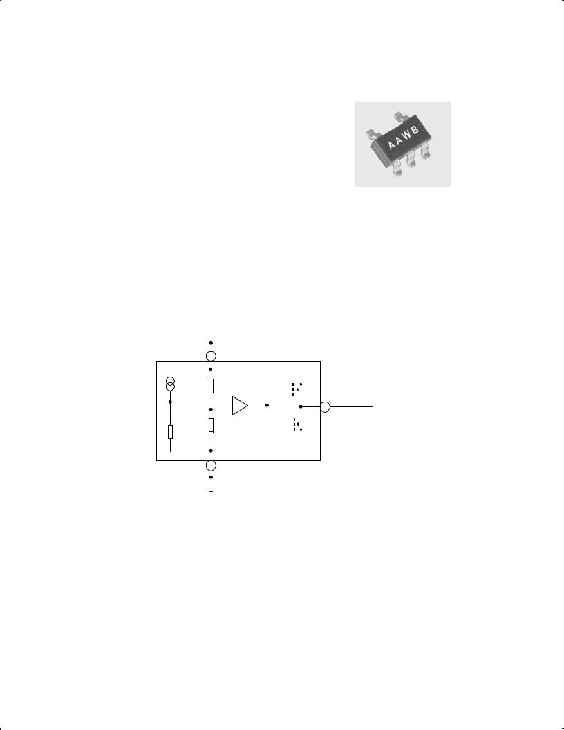
PIN CONFIGURATION |
|
|
|
|
PIN DESCRIPTION |
|
||||
|
|
|
|
|
|
|
PIN |
SYMBOL |
|
DESCRIPTION |
|
|
|
|
|
|
|
|
|
|
|
|
|
|
|
|
|
|
1 |
VOUT |
|
Reset HIGH output. |
VOUT |
1 |
|
|
5 |
N/C |
|||||
|
|
|
2 |
VDD |
|
Positive supply. |
||||
|
|
|
|
|
|
|
|
|||
|
|
|
SA56614-XX |
|
|
|
3 |
VSS |
|
Ground. Negative supply. |
VDD |
2 |
|
|
|
||||||
|
|
|
|
|
|
|
4 |
N/C |
|
No connection. |
|
|
|
|
|
|
|
|
|
|
|
VSS |
|
|
|
|
N/C |
|
5 |
N/C |
|
No connection. |
3 |
|
|
4 |
|||||||
|
|
|
|
|
|
|
|
|
|
|
SL01360
Figure 2. Pin configuration.
MAXIMUM RATINGS
SYMBOL |
PARAMETER |
MIN. |
MAX. |
UNIT |
|
|
|
|
|
VDD |
Power supply voltage |
±0.3 |
12 |
V |
VOUT |
Output voltage |
± |
VSS ± 0.3 |
V |
IOUT |
Output current |
± |
50 |
mA |
Toper |
Operating temperature |
±40 |
85 |
°C |
Tstg |
Storage temperature |
±40 |
125 |
°C |
P |
Power dissipation |
± |
150 |
mW |
|
|
|
|
|
2001 Jun 19 |
3 |

Philips Semiconductors |
Product data |
|
|
|
|
CMOS system reset |
SA56614-XX |
|
|
|
|
DC ELECTRICAL CHARACTERISTICS
Characteristics measured with Tamb = 25 °C, unless otherwise specified.
SYMBOL |
PARAMETER |
CONDITIONS |
TEST |
MIN. |
TYP. |
MAX. |
UNIT |
|
|
|
|
CIRCUIT |
|
|
|
|
|
|
|
|
|
|
|
|
|
|
VS |
Reset detection threshold |
|
|
VS ± 2% |
VS |
VS + 2% |
V |
|
DVS |
Hysteresis |
VDD = 0 V → VS + 1.0 V → 0 V |
1 |
VS × 0.03 |
VS × 0.05 |
VS × 0.08 |
V |
|
VS/DT |
Threshold voltage temperature |
±40 °C ≤ Tamb ≤ +85 °C |
± |
±0.01 |
± |
%/°C |
||
Fig. 16 |
||||||||
|
coefficient |
|
|
|
|
|
|
|
|
|
|
|
|
|
|
|
|
ICC |
Supply current |
VDD = VS + 1.0 V |
|
± |
0.25 |
1.0 |
mA |
|
IOH |
IDS leakage current when OFF |
VDD = VDS = 10 V |
3 |
± |
± |
0.1 |
mA |
|
|
|
|
Fig. 18 |
|
|
|
|
|
|
|
|
|
|
|
|
|
|
INDS1 |
N-channel IDS output sink current 1 |
VDD = 1.2 V; VDS = 0.5 V |
|
±0.23 |
±1.4 |
± |
mA |
|
INDS2 |
N-channel IDS output sink current 2 |
VDS = 0.5 V; VDD = 2.4 V |
2 |
±1.6 |
±8.3 |
± |
mA |
|
|
(for VS > 2.6 V) |
|
Fig. 17 |
|
|
|
|
|
INDS3 |
N-channel IDS output sink current 3 |
VDS = 0.5 V; VDD = 3.6 V |
|
±3.2 |
±14.7 |
± |
mA |
|
|
(for VS > 3.9 V) |
|
|
|
|
|
|
|
IPDS1 |
P-channel IDS output source current 1 |
VDS = 0.5 V; VDD = 4.8 V |
|
0.36 |
2.1 |
± |
mA |
|
|
(for VS < 4.0 V) |
|
|
|
|
|
|
|
IPDS2 |
P-channel IDS output source current 2 |
VDS = 0.5 V; VDD = 6.0 V; |
3 |
0.46 |
2.5 |
± |
mA |
|
|
(for VS < 5.7 V) |
4.0 V < VS < 5.7 V |
Fig. 18 |
|
|
|
|
|
IPDS3 |
P-channel IDS output source current 3 |
VDS = 0.5 V; VDD = 8.4 V |
|
0.59 |
3.3 |
± |
mA |
|
|
(for VS < 5.7 V) |
|
|
|
|
|
|
2001 Jun 19 |
4 |

Philips Semiconductors |
Product data |
|
|
|
|
CMOS system reset |
SA56614-XX |
|
|
|
|
TYPICAL PERFORMANCE CURVES
|
0.50 |
|
|
|
|
|
|
|
|
0.45 |
VDD = VS + 1.0 V |
|
|
|
|
|
|
|
NORMALIZED TO 25 °C |
|
|
|
|
|||
(mA) |
0.40 |
|
|
|
|
|
|
|
|
|
|
|
|
|
|
|
|
CURRENT |
0.35 |
|
|
|
|
|
|
|
0.30 |
|
|
|
|
|
|
|
|
|
|
|
|
|
|
|
|
|
, SUPPLY |
0.25 |
|
|
|
|
|
|
|
0.20 |
|
|
|
|
|
|
|
|
DD |
|
|
|
|
|
|
|
|
I |
|
|
|
|
|
|
|
|
|
0.15 |
|
|
|
|
|
|
|
|
0.10 |
|
|
|
|
|
|
|
|
±50 |
±25 |
0 |
25 |
50 |
75 |
100 |
125 |
|
|
|
|
Tamb, TEMPERATURE (°C) |
|
|
|
|
|
|
|
|
|
|
|
|
SL01344 |
Figure 3. Supply current versus temperature.
(mV) |
200 |
|
|
|
|
|
|
|
|
|
|
|
|
|
|
|
|
|
|
|
|
|
|
|
|
|
|
|
|
|
|
|
|
||
|
|
|
|
|
|
|
|
|
|
|
|
|
|
|
|||
|
|
VS(HYS) = VSH ± VSL |
|
|
|
|
|
|
|
|
|||||||
|
|
(VCC RISING ± VCC FALLING) |
|
|
|
|
|
|
|
|
|||||||
HYSTERESIS |
150 |
|
|
|
|
|
|
|
|
|
|
|
|
|
|
|
|
|
|
|
|
|
|
|
|
|
|
|
|
|
|
|
|
||
|
|
|
|
|
|
|
|
|
|
|
|
|
|
|
|
||
|
|
|
|
|
|
|
|
|
|
|
|
|
|
|
|
|
|
|
|
|
|
|
|
|
|
|
|
|
|
|
|
|
|
|
|
, DETECTION |
100 |
|
|
|
|
|
|
|
|
|
|
|
|
|
|
|
|
|
|
|
|
|
|
|
|
|
|
|
|
|
|
|
|
||
50 |
|
|
|
|
|
|
|
|
|
|
|
|
|
|
|
|
|
|
|
|
|
|
|
|
|
|
|
|
|
|
|
|
|
||
S(HYS) |
|
|
|
|
|
|
|
|
|
|
|
|
|
|
|
|
|
V |
|
|
|
|
|
|
|
|
|
|
|
|
|
|
|
|
|
|
0 |
|
|
|
|
|
|
|
|
|
|
|
|
|
|
|
|
|
|
|
|
|
|
|
|
|
|
|
|
|
|
|
|
|
|
|
±50 |
±25 |
0 |
25 |
50 |
75 |
100 |
125 |
|||||||||
|
|
|
|
|
|
|
|
Tamb, TEMPERATURE (°C) |
|
|
|
|
|
|
|||
|
|
|
|
|
|
|
|
|
|
|
|
|
|
|
|
SL01346 |
|
|
|
|
|
|
|
|
|
|
|
|
|
|
|
|
|
|
|
Figure 5. Detection hysteresis versus temperature.
|
5.0 |
|
|
|
|
|
|
|
|
TAMB = 25 °C |
|
|
|
|
|
|
4.0 |
TYPICAL CHARACTERISTIC. |
|
|
|
|
|
(V) |
DETECTION AND RELEASE |
|
|
|
|
||
|
|
|
|
|
|||
|
VOLTAGE POINTS DEPEND ON |
|
|
|
|||
VOLTAGE |
|
|
|
|
|||
|
THE SPECIFIC DEVICE TYPE. |
|
|
|
|||
3.0 |
|
|
|
VS(HYS) |
|
|
|
|
|
|
|
|
|
||
OUTPUT |
|
|
|
|
) |
) |
|
2.0 |
|
|
|
SL |
SH |
|
|
|
|
|
(V |
(V |
|
||
|
|
|
|
|
|||
, |
|
|
|
|
DETECTION |
RELEASE |
|
OUT |
1.0 |
|
|
|
|
||
V |
|
|
|
|
|||
|
|
|
|
|
|||
|
0 |
|
|
|
|
|
|
|
0 |
1.0 |
2 .0 |
3.0 |
4.0 |
5.0 |
6.0 |
VDD, SUPPLY VOLTAGE (V)
SL01348
Figure 7. Output voltage versus supply voltage.
|
+0.20 |
|
|
|
|
|
|
|
|
|
|
|
|
|
|
|
|
|
|
|
|
|
|
|
|
|
|
|
|
|
|
|
|
|
|
|
|
|
|
|
|
|
|
|
|
|
|
|
|
|
|
|
|
|
|
|
|
+0.15 |
|
|
VCC FALLING |
|
|
|
|
|
|
|
|
|
|
|
|
|
|
(V) |
|
|
VS NORMALIZED TO 25 °C |
|
|
|
|
|
|
|
|
|
|
|||||
|
|
|
|
|
|
|
|
|
|
|
|
|
|
|
|
|
|
|
THRESHOLD |
+0.10 |
|
|
|
|
|
|
|
|
|
|
|
|
|
|
|
|
|
|
|
|
|
|
|
|
|
|
|
|
|
|
|
|
|
|
|
|
|
+0.05 |
|
|
|
|
|
|
|
|
|
|
|
|
|
|
|
|
|
|
|
|
|
|
|
|
|
|
|
|
|
|
|
|
|
|
|
|
NORMALIZED, |
VS |
|
|
|
|
|
|
|
|
|
|
|
|
|
|
|
|
|
|
|
|
|
|
|
|
|
|
|
|
|
|
|
|
|
|
||
±0.05 |
|
|
|
|
|
|
|
|
|
|
|
|
|
|
|
|
|
|
|
|
|
|
|
|
|
|
|
|
|
|
|
|
|
|
|
|
|
S |
±0.10 |
|
|
|
|
|
|
|
|
|
|
|
|
|
|
|
|
|
|
|
|
|
|
|
|
|
|
|
|
|
|
|
|
|
|
||
±0.15 |
|
|
|
|
|
|
|
|
|
|
|
|
|
|
|
|
|
|
|
|
|
|
|
|
|
|
|
|
|
|
|
|
|
|
|
||
V |
|
|
|
|
|
|
|
|
|
|
|
|
|
|
|
|
|
|
|
|
|
|
|
|
|
|
|
|
|
|
|
|
|
|
|
|
|
|
±0.20 |
|
|
|
|
|
|
|
|
|
|
|
|
|
|
|
|
|
|
|
|
|
|
|
|
|
|
|
|
|
|
|
|
|
|
|
|
|
±50 |
±25 |
0 |
25 |
50 |
75 |
100 |
125 |
||||||||||
|
|
|
|
|
|
|
|
Tamb, TEMPERATURE (°C) |
|
|
|
|
|
|
||||
|
|
|
|
|
|
|
|
|
|
|
|
|
|
|
|
|
SL01345 |
|
|
|
|
|
|
|
|
|
|
|
|
|
|
|
|
|
|
|
|
Figure 4. Detection threshold versus temperature.
|
3.0 |
|
|
|
|
|
|
|
|
|
VDS = 0.5 V |
|
|
|
|
|
|
(mA) |
2.5 |
|
|
|
|
|
|
|
|
|
|
|
|
|
|
|
|
CURRENT |
2.0 |
|
|
|
|
|
|
|
|
|
|
N-CHANNEL |
|
|
|
||
1.5 |
|
|
|
|
|
|
|
|
FET |
|
|
|
|
|
|
|
|
|
|
|
|
|
|
|
|
|
, OUTPUT |
1.0 |
|
|
|
|
|
|
|
|
|
|
|
P-CHANNEL |
|
|
|
|
DS |
0.5 |
|
|
|
|
|
|
|
I |
|
|
|
|
|
|
|
|
|
0 |
|
|
|
|
|
|
|
|
±50 |
±25 |
0 |
25 |
50 |
75 |
100 |
125 |
|
|
|
|
Tamb, TEMPERATURE (°C) |
|
|
|
|
|
|
|
|
|
|
|
|
SL01347 |
Figure 6. Output FET current versus temperature.
|
0.6 |
|
|
|
|
|
|
|
|
|
|
|
|
TAMB = 25 °C |
|
|
|
|
|
|
|
|
|
|
0.5 |
|
|
|
|
|
|
|
|
|
|
μA) |
|
|
|
|
|
|
|
|
|
|
|
( |
0.4 |
|
|
|
|
|
|
|
|
|
|
CURRENT |
|
|
|
|
|
|
|
|
|
|
|
0.3 |
|
|
|
|
|
|
|
|
|
|
|
|
|
|
|
|
|
|
|
|
|
|
|
, SUPPLY |
0.2 |
|
|
|
|
|
|
|
|
|
|
|
|
|
|
|
|
|
|
|
|
|
|
DD |
0.1 |
|
|
|
|
|
|
|
|
|
|
I |
|
|
|
|
|
|
|
|
|
|
|
|
|
|
|
|
|
|
|
|
|
|
|
|
0 |
|
|
|
|
|
|
|
|
|
|
|
0 |
1.0 |
2.0 |
3.0 |
4.0 |
5.0 |
6.0 |
7.0 |
8.0 |
9.0 |
10 |
|
|
|
|
VDD, SUPPLY VOLTAGE (V) |
|
|
|
||||
SL01349
Figure 8. Supply current versus supply voltage.
2001 Jun 19 |
5 |
 Loading...