


Technical Guide
Colour Television
GP 31 Chassis
Circuit Explanations
Panasonic
Panasonic AVC Networks
Kuala Lumpur Malaysia Sdn. Bhd.
1
Contents
Introduction |
3 |
||
Location of Control & Circuit Boards |
4 |
||
GP-31 Chassis Block Diagram |
5 |
||
1. |
Tuning Circuit |
|
|
|
1.1 |
Signal Processing |
6 |
|
1.2 |
IF Control |
6 |
2. |
Ultimate One Chip IC601 |
|
|
|
2.1 |
Features |
8 |
|
2.2 |
IIC Bus |
9 |
|
2.3 Memory IC |
9 |
|
|
2.4 |
Reset Circuit |
10 |
|
2.5 |
IC601 Pin Configuration |
11 |
3. |
Video Circuit |
|
|
|
3.1 |
Video Signal Processing |
14 |
4. |
Audio Circuit |
|
|
|
4.1 |
Audio Processor |
17 |
|
|
4.1.1 Sound Processor |
17 |
|
|
4.1.2 Audio Amplifier |
17 |
5. |
Deflection Circuit |
|
|
|
5.1 |
Horizontal Output Circuit |
20 |
|
|
5.1.1 Horizontal Output Operation |
21 |
|
5.2 |
Vertical Output Circuit |
23 |
|
|
5.2.1 Vertical Output Operation |
23 |
6. |
Colour Output |
|
|
|
6.1 |
Colour Output Stage |
24 |
7. |
Protection Circuit |
25 |
|
8. |
Power Circuit |
|
|
|
8.1 |
Start-up Circuit |
29 |
|
8.2 |
Output Voltage Control |
29 |
|
8.3 |
Regulation |
30 |
|
8.4 |
Over Voltage Protection Circuit |
30 |
|
8.5 |
Over Current Protection Circuit |
31 |
|
8.6 |
Latch Circuit |
31 |
|
8.7 |
Standby Operation |
31 |
2

! WARNING
This service information is designed for experienced repair technicians only and is not designed for use by general public. It does not contain warnings or cautions to advise non-technical individuals of potential dangers in attempting to service a product. Products powered by electricity should be serviced or repaired only by experienced professional technicians. Any attempt to service or repair the product or products dealt with in this service information by anyone else could result in serious injury or death.
Introduction
We at Panasonic realise that the service engineer needs to understand the circuitry inside the TV and for this need, we have produced this Technical Guide.
This Technical Guide contains information for GP 31 chassis and should be used in conjunction with the relevant Service Manuals for this chassis.
As the Technical Guide for the GP 31 chassis covers such a wide range of models, some differences may occur in circuit descriptions and component references.
3
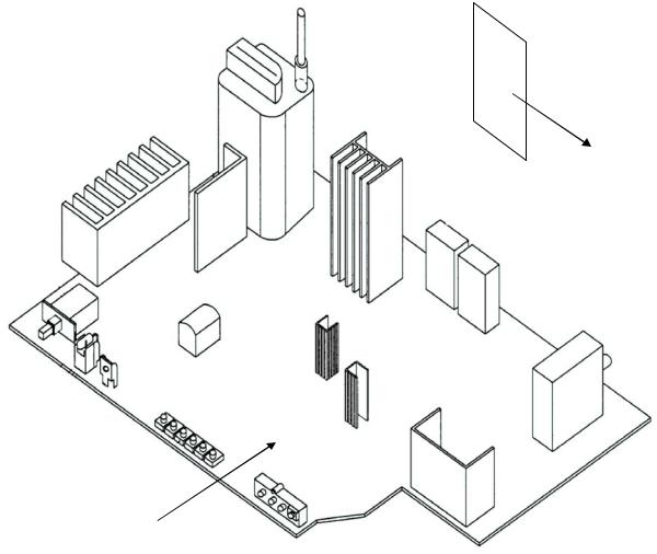
Location of Control & Circuit Boards
L-Board
A- Board
Board Name |
Function |
A-Board |
Main Board |
L-Board |
CRT Board |
4

GP-31 Chassis Block Diagram
5
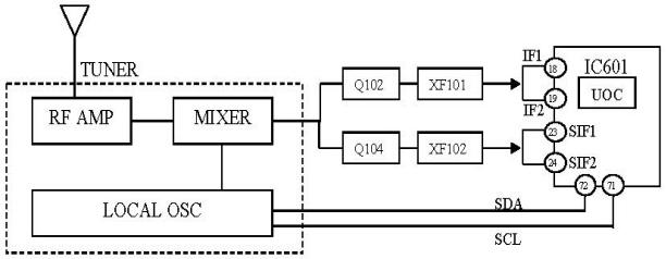
1.Tuning Circuit
Outline
Fig 1.0
The tuner is designed for reception of the conventional frequencies to date and the intermediate special channel frequencies. The IF stage of the tuner contains the video and audio demodulators which are designed for most widely used TV standards.
1.1 Signal Processing
1. The purpose of the tuner is to convert the VHF/ UHF TV broadcast signal (RF) into intermediate frequency signal, IF (38.0MHz) [Fig 1.0].
2. The aerial intercepts the TV signal and amplified by the RF amplifier.
3. The local oscillator generates basic frequency to convert RF signal into IF signal (intermediate signal) in the mixer.
4. Here the IF signals is output to UOC IC601 for video and sound processing.
1.2 IF Control
Control of internal Tuner-IF processing is performed by the UOC IC601, the IC601 sending control information via I²C bus input via pin 71 (SCL) and 72 (SDA).
In addition to this, AGC control of the Tuner-IF stage is controlled by the UOC via I²C. AFC information for Tuner-IF stage is fed back to the IC601 via control line AGC (pin 22).
6

UOC IC601
7
2.Ultimate One Chip IC601
Outline
The IC601 TDA959xN, also known as UOC, is a high-quality single chip TV processors IC which allow the economic integration of features in all classes of singlescan TV sets. UOC combine the functions of a video processor together with a microcontroller and teletext decoder.
The integrated microcontroller is supported by a powerful OSD generator with integrated Teletext & Close Caption acquisition including on-chip page memory.
2.1Features
a.TV Processor
•Multi-standard vision IF circuit
•Picture improvement features with peaking black stretching
•Multi-standard colour decoder with automatic search system
•Internal base-band delay line
•Horizontal and vertical geometry processing
•OSD/text gain reduction control
•White point and black level off-set adjustment
b.Micro-controller
•80C51 micro-controller core standard instruction set and timing
•1 µs machine cycle
•128K-byte ROM
•12K-byte RAM
•Data Back-up
Storage of tuning, switching, control and adjustment data to the memory (IC1103) and reading out the data
•Switching and Control
Output of the control signal for picture and sound, etc., and switching signal for TV/AV mode and so on
•Adjustment
Output of adjustment levels for UOC (IC601) through I²C bus.
c.Teletext Decoder
•Text memory for 1 or 10 pages
•Automatic detection of FASTEXT transmission
•Data Capture for US Closed Caption
8
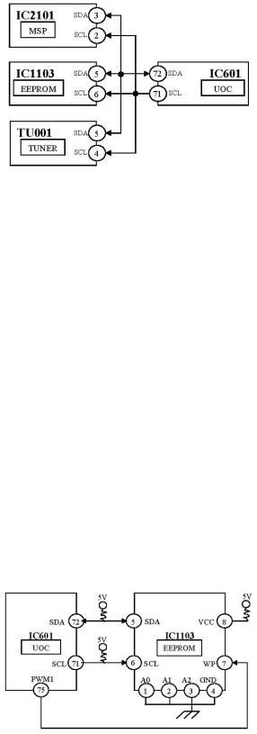
2.2I²C bus
Fig 2.0
•The I²C bus is a two bus system consisting of a data line and a clock line.
•5V is set for SDA / SCL. [Fig 2.0]
•Allow a large number of switching and control functions of GP-31 chassis.
The UOC IC601 generates bus signals which control the following hardware configuration.
1. EEPROM IC1103
These memories are 1K-byte, non-volatile memories of microchips, and bit pattern of 1024 x 8 bits.
2.Tuner TU001
To select a desired channel signal from the several RF signal from TV stations and
convert the selected RF signal into a signal of an intermediate frequency (IF).
3. Sound Processor IC2101
The sound processor IC will cover the sound processing of all analog TV-Standards worldwide, as well as the NICAM digital sound standards.
2.3Memory IC
Fig 2.1
9
The memory IC1103 receives the data listed below as supplied from the UOC IC601 through I²C bus [Fig 2.1]. It is input or output whenever it is necessary. This memory IC is a non-volatile type, which data is maintained permanently although the power is cut off.
Last Memory Location
These memory locations will contain the following information that must be stored inside even if power to the EEPROM is interrupted.
1.100 channels of BT voltage and band (VL, VH, U) information.
2.100 channels of AFC, SKIP, COLOR SYSTEM and SIF information.
3.Last position for each switching mode.
4.Volume data.
5.TV/ AV1/ AV2 mode.
6.Recall ON/ OFF.
7.Power and auto off timer setting.
8.Service mode setting.
9.The COLOUR, NTSC TINT, BRIGHT, CONTRAST and SHARPNESS DAC data, and each SUB-DAC data, CUT-OFF, RGB-DRIVE etc.
10.PICTURE MENU & SOUND MENU.
11.AVL
Pin No. |
Name |
Function |
1 |
A0 |
GROUND |
2 |
A1 |
GROUND |
3 |
A2 |
GROUND |
4 |
GND |
GROUND |
5 |
SDA |
Serial Data In/Out |
6 |
SCL |
Serial Clock Input |
7 |
WP |
Write Protect Input |
8 |
VCC |
5V |
2.4Reset circuit
1.Power on reset is generated internally to the UOC IC601; hence no external reset is required. (The TV processor generates the master reset in the system, which in turn will reset the micro-controller.)
2.During power ON operation, or during a momentary drop in the +B voltage, insufficient voltage supply to UOC IC601 may occur. Thus, there is a possibility that incorrect operation of the UOC occur.
3.In order to prevent incorrect operation, a resetting pulse is activated until the voltage fed to the UOC is normalized.
4.When the power switch is turned on, if the VDD of the UOC is less than 3.3V then UOC starts to reset.
5.UOC start to function again when VDD becomes more than 3.3V.
10
 Loading...