


OMNIREL OM6227SS, OM6231SS, OM6230SS, OM6232SS, OM6233SS Datasheet
...
3.1 - 123
3.1
400V, 500V, 1000V, Up To 24 Amp N-Channel,
Dual Size 6 High Energy MOSFETs
4 11 R2
Supersedes 2 07 R1
DUAL HIGH CURRENT POWER MOSFETS
IN HERMETIC ISOLATED SIP PACKAGE
OM6232SS
OM6233SS
OM6230SS
OM6231SS
OM6227SS
OM6228SS
FEATURES
• Dual Uncommitted MOSFETs
• Isolated Hermetic Metal Package
• Size 6 Die, High Energy, High Voltage
• Fast Switching, Low Drive Current
• Ease of Paralleling For Added Power
• Low R
DS(on)
• Available Screened to MIL-S-19500, TX, TXV And S Levels
DESCRIPTION
This series of hermetically packaged products feature the latest advanced MOSFET
and packaging technology. They are ideally suited for Military requirements where
small size, high performance and high reliability are required, and in applications
such as switching power supplies, motor controls, inverters, choppers, audio
amplifiers and high energy pulse circuits. This series also features avalanche high
energy capability at elevated temperatures.
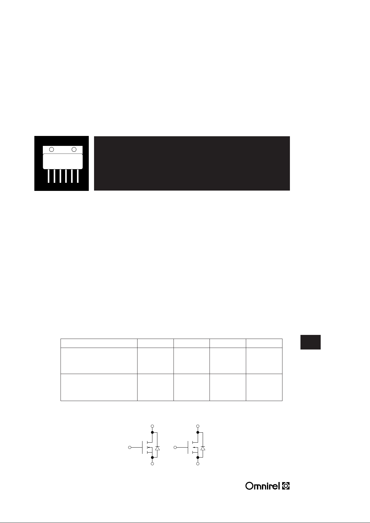
MAXIMUM RATINGS
PART NUMBER V
DS
R
DS(on)
ID (Amp) *Package
OM6227SS 400 .20 24 S-6D
OM6228SS 500 .27 22 S-6D
OM6230SS 1000 1.30 10 S-6D
OM6231SS 400 .20 24 S-6E
OM6232SS 500 .27 22 S-6E
OM6233SS 1000 1.30 10 S-6E
* See Mechanical Drawing
1
3
2
4
6
5SOURCESOURCE
DRAIN DRAIN
GATEGATE
BODY
DIODE
BODY
DIODE
SCHEMATIC
3.1 - 124
OM6227SS - OM6233SS
3.1
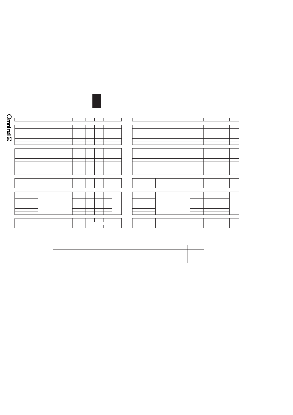
UNCLAMPED DRAIN-TO-SOURCE AVALANCHE CHARACTERISTICS (TJ< 150°)
Symbol Value Unit
Single Pulse Drain-To-Source Avalanche Energy TJ= 25°C
W
DSS
(1)
1000
TJ= 100°C 160 mJ
Repetitive Pulse Drain-To-Source Avalanche Energy W
DSS
(2) 25
(1) VDD= 50V, ID= 10A
(2) Pulse width and frequency is limited by T
J(max)
and thermal response.
ELECTRICAL CHARACTERISTICS: 400V (Per MOSFET) (T
C
= 25° unless otherwise noted)
Characteristic Symbol Min. Typ. Max. Unit
OFF CHARACTERISTICS
Drain-Source Breakdown Voltage (VGS= 0, ID= 0.25 mA) V
(BR)DSS
400 - - Vdc
Zero Gate Voltage Drain I
DSS
mAdc
(VDS= 400 V, VGS= 0) - - 0.25
(VDS= 320 V, VGS= 0, TJ= 125° C) - - 1.0
Gate-Body Leakage Current, Forward (V
GSF
= 20 Vdc, VDS= 0) I
GSSF
- - 100 nAdc
Gate-Body Leakage Current, Reverse (V
GSR
= 20 Vdc, VDS= 0) I
GSSR
- - 100 nAdc
ON CHARACTERISTICS*
Gate-Threshold Voltage V
GS(th)
Vdc
(VDS= VGS, ID= 0.25 mAdc 2.0 3.0 4.0
(TJ= 125° C) 1.5 - 3.5
Static Drain-Source On-Resistance (VGS= 10 Vdc, ID= 13 Adc) r
DS(on)
- - 0.20 Ohm
Drain-Source On-Voltage (VGS= 10 Vdc) V
DS(on)
Vdc
(ID= 24 A) - - 5.0
(ID= 12 A, TJ= 125° C) - - 5.0
Forward Transconductance (VDS= 15 Vdc, ID= 12A Adc) g
FS
14 - - mhos
DYNAMIC CHARACTERISTICS
Input Capacitance (VDS= 25 V, VGS= 0, C
iss
- 4000 - pF
Output Capacitance f = 1.0 MHz) C
oss
- 550 -
Transfer Capacitance C
rss
- 110 -
SWITCHING CHARACTERISTICS
Turn-On Delay Time t
d(on)
-35-ns
Rise Time (VDD= 250 V, ID= 24 A, t
r
-95-
Turn-Off Delay Time R
gen
= 4.3 ohms) t
d(off)
-80-
Fall Time t
f
-80-
Total Gate Charge (VDS= 400 V, ID= 24 A, Q
g
- 110 14 0nC
Gate-Source Charge VGS= 10 V) Q
gs
-20-
Gate-Drain Charge Q
gd
-80-
SOURCE DRAIN DIODE CHARACTERISTICS
Forward On-Voltage V
SD
- 1.1 1.6 Vdc
Forward Turn-On Time (IS= 24 A, d/dt = 100 A/µs) t
on
**
ns
Reverse Recovery Time t
rr
- 500 1000
ELECTRICAL CHARACTERISTICS: 500V (Per MOSFET) (T
C
= 25° unless otherwise noted)
Characteristic Symbol Min. Typ. Max. Unit
OFF CHARACTERISTICS
Drain-Source Breakdown Voltage (VGS= 0, ID= 0.25 mA) V
(BR)DSS
500 - - Vdc
Zero Gate Voltage Drain I
DSS
mAdc
(VDS= 500 V, VGS= 0) - - 0.25
(VDS= 500 V, VGS= 0, TJ= 125° C) - - 1.0
Gate-Body Leakage Current, Forward (V
GSF
= 20 Vdc, VDS= 0) I
GSSF
- - 100 nAdc
Gate-Body Leakage Current, Reverse (V
GSR
= 20 Vdc, VDS= 0) I
GSSR
- - 100 nAdc
ON CHARACTERISTICS*
Gate-Threshold Voltage V
GS(th)
Vdc
(VDS= VGS, ID= 0.25 mAdc 2.0 3.0 4.0
(TJ= 125° C) 1.5 - 3.5
Static Drain-Source On-Resistance (VGS= 10 Vdc, ID= 13 Adc) r
DS(on)
- - 0.27 Ohm
Drain-Source On-Voltage (VGS= 10 Vdc) V
DS(on)
Vdc
(ID= 24 A) - - 8.0
(ID= 12 A, TJ= 125° C) - - 8.0
Forward Transconductance (VDS= 15 Vdc, ID= 13 Adc) g
FS
13 - - mhos
DYNAMIC CHARACTERISTICS
Input Capacitance (VDS= 25 V, VGS= 0, C
iss
- 4000 - pF
Output Capacitance f = 1.0 MHz) C
oss
- 480 -
Transfer Capacitance C
rss
-95-
SWITCHING CHARACTERISTICS
Turn-On Delay Time t
d(on)
-32-ns
Rise Time (VDD= 250 V, ID= 24 A, t
r
-95-
Turn-Off Delay Time R
gen
= 4.3 ohms) t
d(off)
-75-
Fall Time t
f
-75-
Total Gate Charge (VDS= 400 V, ID= 24 A, Q
g
- 115 140 nC
Gate-Source Charge VGS= 10 V) Q
gs
-20-
Gate-Drain Charge Q
gd
-60-
SOURCE DRAIN DIODE CHARACTERISTICS
Forward On-Voltage V
SD
- 1.1 1.6 Vdc
Forward Turn-On Time (IS= 24 A, d/dt = 100 A/µs) t
on
**
ns
Reverse Recovery Time t
rr
- 500 1000
* Indicates Pulse Test = 300 µsec, Duty Cycle = 2%
** Limited by circuit inductance
* Indicates Pulse Test = 300 µsec, Duty Cycle = 2%
** Limited by circuit inductance
 Loading...