


OMNIREL OM6038SM, OM6054SJ, OM6050SJ, OM6041SM, OM6040SM Datasheet
...
3.1 - 105
3.1
High Current, High Voltage 100V Thru 1000V,
Up To 100 Amp N-Channel, Size 7 MOSFETs,
High Energy Capability
HIGH CURRENT MOSFET IN ISOLATED, TO-267
HERMETIC PACKAGE, SIZE 7 DIE, LOW R
DS(on)
FEATURES
• Isolated Hermetic Metal Package
• Size 7 Die, High Energy
• Fast Switching, Low Drive Current
• Ease Of Paralleling For Added Power
• Low R
DS(on)
• Available Screened To MIL-S-19500, TX, TXV And S Levels
DESCRIPTION
This series of hermetically packaged products feature the latest advanced MOSFET
and packaging technology. They are ideally suited for Military requirements where
small size, high performance and high reliability are required, and in applications such
as switching power supplies, motor controls, inverters, choppers, audio amplifiers and
high energy pulse circuits. This series also features avalanche high energy capability
at elevated temperatures.
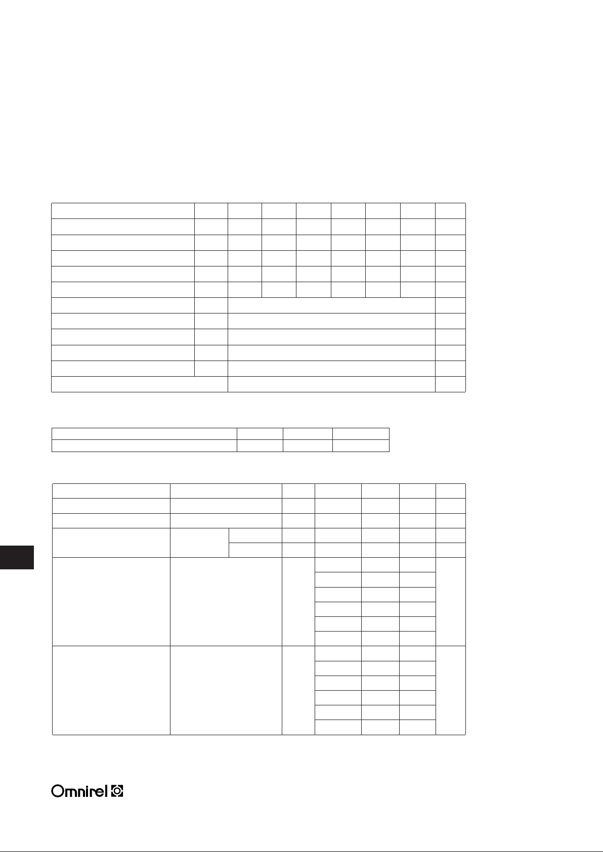
MAXIMUM RATINGS
@ 25°C
4 11 R0
OM6054SJ
OM6055SJ
OM6052SJ
OM6053SJ
OM6050SJ
OM6051SJ
PART NUMBER V
DS
R
DS(on)
ID(Continuous)
OM6050SJ 100 V .014 100 A
OM6051SJ 200 V .030 55 A
OM6052SJ 500 V .160 30 A
OM6053SJ 600 V .230 25 A
OM6054SJ 800 V .500 18 A
OM6055SJ 1000 V .800 10 A
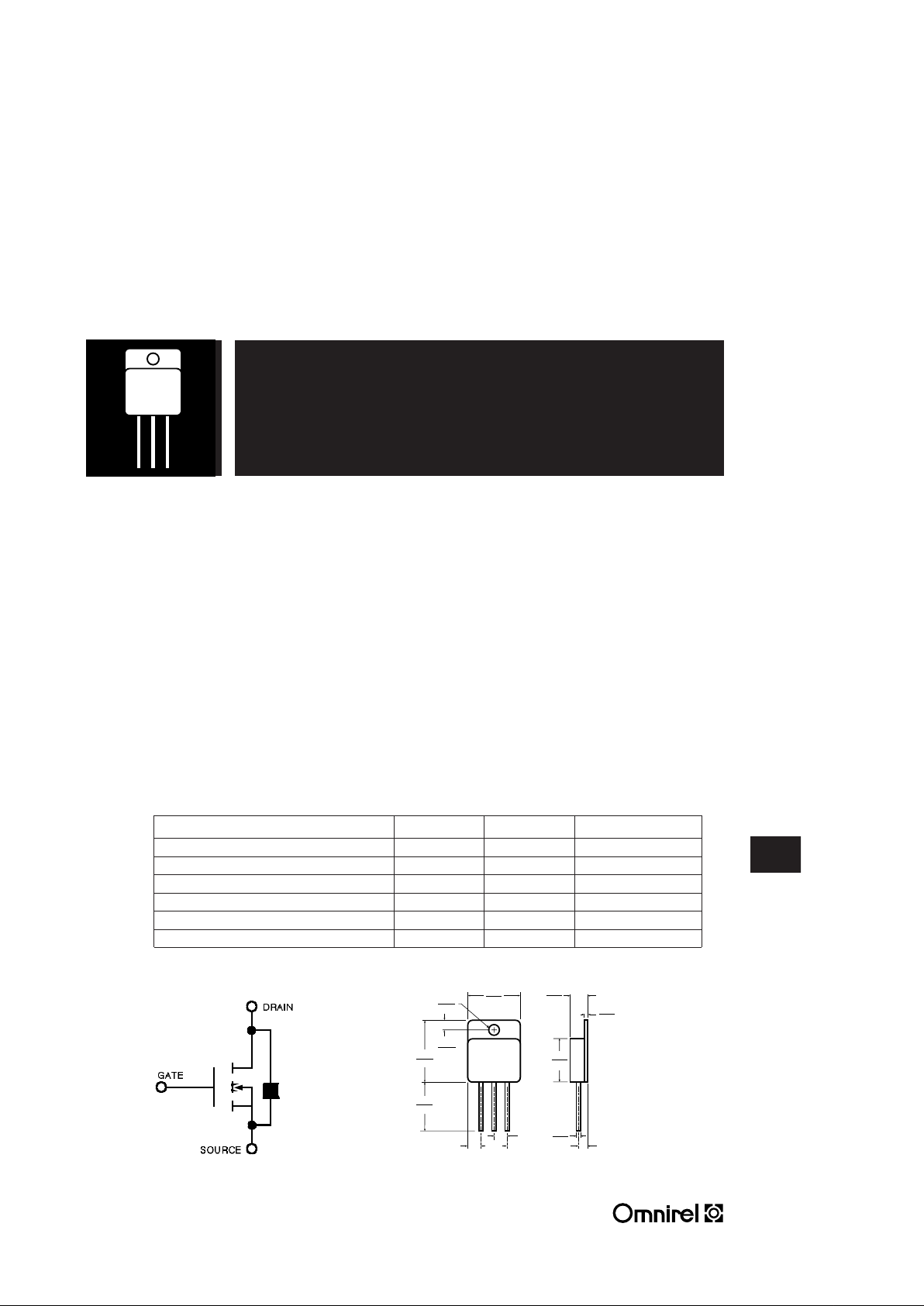
SCHEMATIC MECHANICAL OUTLINE
.950
.930
.150
.140
.750
.500
.805
.795
.200
.400
.200
ø
.165
.155
.665
.645
.160
.290
.260
.065
.055
.065
.055
ø
1
3
2
123
TO-267
3.1
205 Crawford Street, Leominster, MA 01453 USA (508) 534-5776 FAX (508) 537-4246
OM6050SJ - OM6055SJ
ABSOLUTE MAXIMUM RATINGS (T
C
= 25 C unless otherwise noted)
Parameter Symbol OM6050SJ OM6051SJ OM6052SJ OM6053SJ OM6054SJ OM6055SJ Unit
Drain Source Voltage V
DS
100 200 500 600 800 1000 V
Drain Gate Voltage (R
GS
= 1.0 M ) V
DGR
100 200 500 600 800 1000 V
Continuous Drain Current @ T
C
= 25°C
2
I
D
100 55 30 25 18 10 A
Continuous Drain Current @ TC = 100°C
2
I
D
43 23 13 10 7 4 A
Pulsed Drain Current
1
I
DM
235 135 80 75 50 30 A
Max. Power Dissipation @ T
C
= 25°C P
D
280 W
Max. Power Dissipation @ T
C
= 100°C P
D
110 W
Linear Derating Factor Junction-to-Case 2.22 W/°C
Linear Derating Factor Junction-to-Ambient .025 W/°C
Operating and Storage Temp. Range T
J
, T
stg
-55 to +150 ° C
Lead Temperature (1/16" from case for 10 sec.) 275 ° C
Notes: 1. Pulse Test: Pulse Width £ 300 msec, Duty Cycle £ 2%. 2. Package Pin Limitation: 35 Amps.
THERMAL RESISTANCE (MAXIMUM) @ T
A
= 25 C
Junction-to-Case R
thJC
.45 ° C/W
Junction-to-Ambient (Free Air Operation) R
thJA
40 ° C/W
PRELIMINARY ELECTRICAL CHARACTERISTICS (T
C
= 25°C unless otherwise noted)
Characteristic Test Condition Symbol Part No. Min. Max. Units
Gate Threshold Voltage V
DS
= VGS, ID= 250µA V
GS(th)
All 2.0 4.0 V
Gate Source Leakage Current V
GS
= ±20 V
DC
I
GSS
All ±100 nA
Off State Drain-Source Leakage V
DS
= V
DSS
x 0.8 TC= 25°C I
DSS
All 10 µA
V
GS
= 0V TC= 125°C I
DSS
All .10 mA
OM6050SJ 100
OM6051SJ 200
Drain-Source Breakdown Voltage V
GS
= 0V, ID= 250 µA V
DSS
OM6052SJ 500
V
OM6053SJ 600
OM6054SJ 800
OM6055SJ 1000
OM6050SJ .014
OM6051SJ .030
Drain-Source Breakdown Voltage V
GS
= 10V, ID= I
D25
x 0.5 R
DS(on)
OM6052SJ .160
OM6053SJ .230
OM6054SJ .500
OM6055SJ .800
The above data is preliminary. Please contact factory for additional data
and the dynamic and switching characteristics.
 Loading...