


OMNIREL OM6060SB, OM6058SB, OM6057SB, OM6056SB, OM6061SB Datasheet
...
3.1 - 107
3.1
High Current, High Voltage 100V Thru 1000V,
Up To 190 Amp N-Channel, Size 7 MOSFETs
POWER MOSFETS IN A HERMETIC ISOLATED
POWER BLOCK PACKAGE
4 11 R0
OM6060SB
OM6061SB
OM6058SB
OM6059SB
OM6056SB
OM6057SB
Preliminary Data Sheet
FEATURES
• Size 7 Die, High Energy
• Rugged Package Design
• Solder Terminals
• Very Low R
DS(on)
• Fast Switching, Low Drive Current
• Available Screened To MIL-S-19500, TX, TXV And S Levels
• Ceramic Feedthroughs
DESCRIPTION
This series of hermetically packaged products feature the latest advanced MOSFET
technology combined with a package designed specifically for high efficiency, high current
applications. They are ideally suited for Hi-Rel requirements where small size, high
performance and high reliability are required, and in applications such as switching power
supplies, motor controls, inverters, choppers, audio amplifiers and high energy pulse circuits.
This series also features avalanche high energy capability at elevated temperatures.
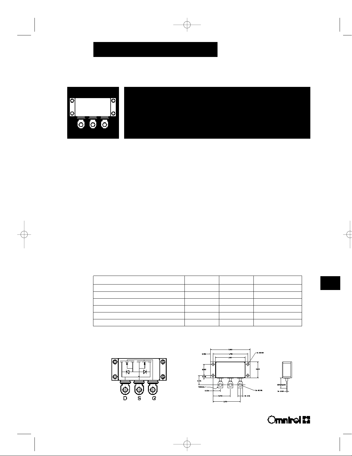
MAXIMUM RATINGS
@ 25°C
PART NUMBER V
DS
R
DS(on)
ID(Continuous)
OM6056SB 100 V .008 Ω 190 A
OM6057SB 200 V .018 Ω 105 A
OM6058SB 500 V .095 Ω 58 A
OM6059SB 600 V .140 Ω 48 A
OM6060SB 800 V .300 Ω 34 A
OM6061SB 1000 V .500 Ω 18 A
PIN CONNECTION MECHANICAL OUTLINE
AND SCHEMATIC
Sect. 3.1 data sheets 8/7/00 11:52 AM Page 107
3.1
OM6056SB - OM6061SB
ABSOLUTE MAXIMUM RATINGS (T
C
= 25°C unless otherwise noted)
Parameter Symbol OM6056SB OM6057SB OM6058SB OM6059SB OM6060SB OM6061SB Unit
Drain Source Voltage V
DS
100 200 500 600 800 1000 V
Drain Gate Voltage (R
GS
= 1.0 MΩ)V
DGR
100 200 500 600 800 1000 V
Continuous Drain Current @ T
C
= 25°C
2
I
D
190 105 58 48 34 18 A
Continuous Drain Current @ TC = 100°C
2
I
D
82 44 25 19 15 7.5 A
Pulsed Drain Current
1
I
DM
440 250 130 110 78 42 A
Max. Power Dissipation @ T
C
= 25°C P
D
570 W
Max. Power Dissipation @ T
C
= 100°C P
D
245 W
Linear Derating Factor Junction-to-Case 4.35 W/°C
Linear Derating Factor Junction-to-Ambient .033 W/°C
Operating and Storage Temp. Range T
J
, T
stg
-55 to +150 ° C
Lead Temperature (1/16" from case for 10 sec.) 230 ° C
Notes: 1. Pulse Test: Pulse Width ≤ 300 µsec, Duty Cycle ≤ 2%. 2. Package Pin Limitation: 100 Amps @ 125°C.
THERMAL RESISTANCE (MAXIMUM) @ T
A
= 25°C
Junction-to-Case R
thJC
.23 ° C/W
Junction-to-Ambient (Free Air Operation) R
thJA
30 ° C/W
PRELIMINARY ELECTRICAL CHARACTERISTICS (T
C
= 25°C unless otherwise noted)
Characteristic Test Condition Symbol Part No. Min. Max. Units
Gate Threshold Voltage V
DS
= VGS, ID= 250µA V
GS(th)
All 2.0 4.0 V
Gate-Source Leakage Current V
GS
= ±20 V
DC
I
GSS
All ±100 nA
Off State Drain-Source Leakage V
DS
= V
DSS
x 0.8 TC= 25°C I
DSS
All 10 µA
V
GS
= 0V TC= 125°C I
DSS
All .10 mA
OM6056SB 100
OM6057SB 200
Drain-Source Breakdown Voltage V
GS
= 0V, ID= 250 µA V
DSS
OM6058SB 500
V
OM6059SB 600
OM6060SB 800
OM6061SB 1000
OM6056SB .008
OM6057SB .018
Static Drain-Source On-Resistance V
GS
= 10V, ID= I
D25
x 0.5 R
DS(on)
OM6058SB .095
Ω
OM6059SB .140
OM6060SB .300
OM6061SB .500
The above data is preliminary. Please contact factory for additional data
and the dynamic and switching characteristics.
Sect. 3.1 data sheets 8/7/00 11:52 AM Page 108
 Loading...