


POWER MOSFETS IN HERMETIC ISOLATED
JEDEC TO-254AA SIZE 6 DIE
400V, 500V, N-Channel, Up To 24 Amp
Size 6 MOSFETs, High Energy Capability
FEATURES
• Isolated Hermetic Metal Package
• Size 6 Die, High Energy
• Fast Switching, Low Drive Current
• Ease of Paralleling For Added Power
• Low R
• Available Screened To MIL-S-19500, TX, TXV And S Levels
DESCRIPTION
This series of hermetically packaged products feature the latest advanced MOSFET
and packaging technology. They are ideally suited for Military requirements where
small size, high performance and high reliability are required, and in applications such
as switching power supplies, motor controls, inverters, choppers, audio amplifiers and
high energy pulse circuits. This series also features avalanche high energy capability
at elevated temperatures.
DS(on)
OM6025SA
OM6026SA
4 11 R0
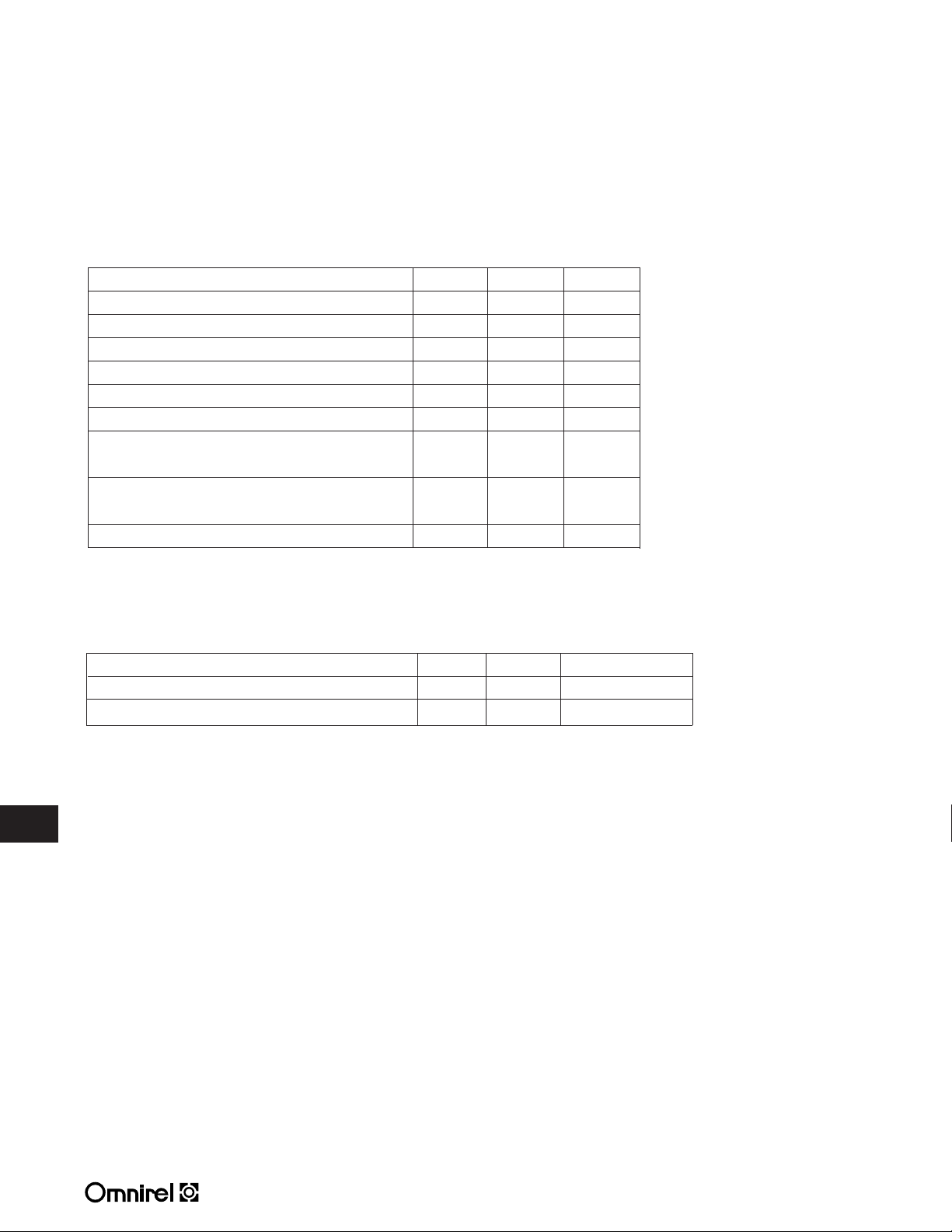
MAXIMUM RATINGS
PART NUMBER V
OM6025SA 400 .23 24
OM6026SA 500 .30 22
DS
SCHEMATIC
3.1 - 93
R
DS(on)
ID (Amp)
3.1
OM6025SA - OM6026SA
ABSOLUTE MAXIMUM RATINGS (TC= 25°C unless otherwise noted)
V
DS
V
DGR
ID@ TC= 25°C Continuous Drain Current
I
DM
PD@ TC= 25°C Maximum Power Dissipation 165 165 W
W
(1) (2) Single Pulse Energy
DSS
T
J
T
stg
Lead Temperature (1/8" from case for 5 secs.) 275 275 °C
Note 1: VDD= 50V, ID= as noted
Note 2: Package Pin Limitation ID@ TC= 25°C = 25 Amps
THERMAL RESISTANCE (MAXIMUM) at TA= 25°C
R
thJC
R
thJA
Parameter OM6025SA OM6026SA Units
Drain-Source Voltage 400 500 V
Drain-Gate Voltage (RGS= 1 M ) 400 500 V
Pulsed Drain Current
2
2
24 22 A
92 85 A
Derate Above 25°C Ambient .025 .025 W/°C
Drain To Source @ 25°C 1000 1200 mJ
Operating and
Storage Temperature Range -55 to 150 -55 to 150 °C
Junction-to-Case .76 °C/W
Junction-to-Ambient 40 °C/W Free Air Operation
Derate Above 25°C Case 1.32 W/°C
3.1
3.1 - 94

OM6025SA - OM6026SA
mAdc
400 - - Vdc
DSS
(BR)DSS
= 25° unless otherwise noted)
C
= 0.25 mA) V
D
= 0, I
GS
= 125° C) - - 1.0
J
= 0) - - 0.25
= 0, T
GS
GS
Characteristic Symbol Min. Typ. Max. Unit
= 400 V, V
= 400 V, V
DS
DS
(V
(V
Drain-Source Breakdown Voltage (V
ELECTRICAL CHARACTERISTICS: OM6025SA (T
Zero Gate Voltage Drain I
OFF CHARACTERISTICS
Vdc
- - 100 nAdc
- - 100 nAdc
GS(th)
GSSF
GSSR
= 0) I
= 0) I
DS
DS
= 20 Vdc, V
= 20 Vdc, V
GSR
GSF
Gate-Body Leakage Current, Forward (V
Gate-Body Leakage Current, Reverse (V
Gate-Threshold Voltage V
ON CHARACTERISTICS*
Vdc
- - 0.23 Ohm
DS(on)
DS(on)
= 12 Adc) r
D
= 10 Vdc, I
GS
= 10 Vdc) V
GS
= 0.25 mAdc 2.0 3.0 4.0
D
, I
GS
= V
= 125° C) 1.5 - 3.5
DS
(V
= 24 A) - - 5.6
J
D
(T
(I
Static Drain-Source On-Resistance (V
Drain-Source On-Voltage (V
- 5600 - pF
-78-
14 - - mhos
FS
= 12 Adc) g
D
= 15 Vdc, I
DS
= 125° C) - - 5.6
J
= 12 A, T
D
(I
Forward Transconductance (V
- 230 -
iss
rss
oss
= 0, C
GS
= 25 V, V
DS
Input Capacitance (V
Output Capacitance f = 1.0 MHz) C
Transfer Capacitance C
DYNAMIC CHARACTERISTICS
SWITCHING CHARACTERISTICS
-70-ns
- 190 -
r
d(on)
= 24 A, t
D
= 250 V, I
DD
Turn-On Delay Time t
Rise Time (V
- 160 -
- 160 -
f
d(off)
= 4.3 ohms) t
gen
Turn-Off Delay Time R
Fall Time t
ns
**
- 110 140 nC
-20-
-55-
- 1.1 1.6 Vdc
- 500 1000
g
gs
= 24 A, Q
D
= 10 V) Q
GS
= 400 V, I
DS
Total Gate Charge (V
Gate-Source Charge V
gd
Gate-Drain Charge Q
rr
SD
on
= 24 A, d/dt = 100 A/µs) t
S
Forward On-Voltage V
Forward Turn-On Time (I
Reverse Recovery Time t
SOURCE DRAIN DIODE CHARACTERISTICS
mAdc
500 - - Vdc
DSS
(BR)DSS
= 25° unless otherwise noted)
C
= 0.25 mA) V
D
= 0, I
GS
= 125° C) - - 1.0
J
= 0) - - 0.25
= 0, T
GS
GS
Characteristic Symbol Min. Typ. Max. Unit
= 500 V, V
= 500 V, V
DS
DS
(V
(V
Drain-Source Breakdown Voltage (V
ELECTRICAL CHARACTERISTICS: OM6026SA (T
Zero Gate Voltage Drain I
OFF CHARACTERISTICS
Vdc
- - 100 nAdc
- - 100 nAdc
GS(th)
GSSF
GSSR
= 0) I
= 0) I
DS
DS
= 20 Vdc, V
= 20 Vdc, V
GSR
GSF
Gate-Body Leakage Current, Forward (V
Gate-Body Leakage Current, Reverse (V
Gate-Threshold Voltage V
ON CHARACTERISTICS*
Vdc
- - 0.30 Ohm
DS(on)
DS(on)
= 11 Adc) r
D
= 10 Vdc, I
GS
= 10 Vdc) V
GS
= 0.25 mAdc 2.0 3.0 4.0
D
, I
GS
= V
= 125° C) 1.5 - 3.5
DS
(V
= 22 A) - - 8.0
J
D
(T
(I
Static Drain-Source On-Resistance (V
Drain-Source On-Voltage (V
- 5600 - pF
- 680 -
11 - - mhos
FS
= 11 Adc) g
D
= 15 Vdc, I
DS
= 125° C) - - 8.0
J
= 11 A, T
D
(I
Forward Transconductance (V
- 200 -
iss
rss
oss
= 0, C
GS
= 25 V, V
DS
Input Capacitance (V
Output Capacitance f = 1.0 MHz) C
Transfer Capacitance C
DYNAMIC CHARACTERISTICS
SWITCHING CHARACTERISTICS
-70-ns
- 190 -
r
d(on)
= 22 A, t
D
= 250 V, I
DD
Turn-On Delay Time t
Rise Time (V
- 160 -
- 160 -
d(off)
= 10 V t
= 4.3 ohms) T
gen
Turn-Off Delay Time R
Fall Time V
- 115 140 nC
-20-
g
f
gs
= 22 A, Q
D
= 10 V) Q
GS
GS
= 400 V, I
DS
Total Gate Charge (V
Gate-Source Charge V
ns
**
-60-
- 1.1 1.6 Vdc
- 500 1000
gd
Gate-Drain Charge Q
rr
SD
on
= 22A, d/dt = 100 A/µs) t
S
Forward On-Voltage V
Forward Turn-On Time (I
Reverse Recovery Time t
* Indicates Pulse Test = 300 µsec, Duty Cycle = 2%
SOURCE DRAIN DIODE CHARACTERISTICS
** Limited by circuit inductance
3.1
3.1 - 95

OM6025SC - OM6026SC
205 Crawford Street, Leominster, MA 01 453 USA (508) 534-5776 FAX (508) 537-4246
.144 DIA.
.050
.040
.260
.249
.685
.665
.800
.790
.545
.535
.550
.510
.045
.035
.550
.530
.150 TYP.
.150 TYP.
.005
.040 DIA.
3 PLCS.
.150
.260
MAX
.040
.940
.500
MIN.
.150
.125
2 PLCS.
.290
.125 DIA.
2 PLS.
.200
.540
.250
.740
.540
.100
2 PLCS.
.300
PIN CONNECTION MECHANICAL OUTLINE
123
1.1
1.2
1.3
1.4
1.5
2.1
3.1
2.3
2.4
Pin 1: Drain
Pin 2: Source
Pin 3: Gate
M-3S
123
Pin 1: Drain
Pin 2: Source
Pin 3: Gate
M-PAK
PACKAGE OPTIONS
3.1
3.2
MOD PAK Z-TAB 6 PIN SIP
NOTES:
• Standard Products are supplied with glass feedthroughs. For ceramic feedthroughs, add the letter “C” to the part number. Example - OMXXXXCSA.
• MOSFETs are also available in Z-Tab, dual and quad pak styles - Please call the factory for more information.
 Loading...