

OM3910STM/NTM
OM3911STM/NTM
3.0 AMP POSITIVE ADJUSTABLE VOLTAGE REGULA TOR
APPROVED TO DESC DRAWING 5962-87675
Three T erminal, Adjustable V oltage, 3.0 Amp
Precision Positive Regulator In Hermetic
JEDEC TO-257AA Package
FEATURES
• Approved To DESC Standardized Military Drawing
5962-8767501UX/TX and 5962-8767502UX/TX
• Isolated Hermetic Package, JEDEC TO-257AA Outline
• Reference Voltages Set To ±1% and ±2%
• Built-In Thermal Overload Protection
• Short Circuit Current Limiting
• Similar Electrically To Industry Standard LM150A
DESCRIPTION
These three terminal positive regulators approved by DESC, are supplied in
a hermetically sealed isolated, metal TO-257 package. All protective features
are designed into the circuit including thermal shutdown, current limiting and safearea control. With heat sinking, they can deliver over 3.0 amps of output current.
These units feature 1% and 2% initial voltage tolerance, 0.35% load regulation and
.01% line regulation.
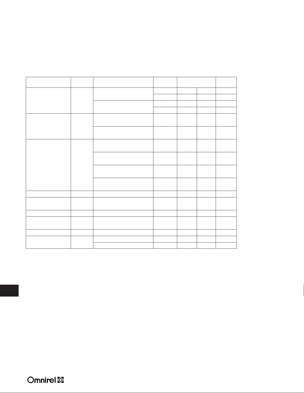
ABSOLUTE MAXIMUM RATINGS
Input - Output Voltage Differential........................................+35 V
Operating Junction Temperature Range........................- 55°C to + 150°C
Storage Temperature Range .................................- 65°C to + 150°C
Typical Power/Thermal Characteristics:
Rated Power @ 25°C
TC...............................................................25 W
TA................................................................3 W
Thermal Resistance:
q
Case U.....................................................4.2°C/W
JC
q
Case T.....................................................3.5°C/W
JC
qJA............................................................50°C/W
a
DESC REFERENCE OMNIREL
DRAWING VOLTAGE PART NUMBER
5962-8767501UX ±2% OM3910STM
5962-8767502UX ±1% OM3911STM
5962-8767501TX ±2% OM3910NTM
5962-8767502TX ±1% OM3911NTM
@ 25°C
3.3
4 11 R1
Supersedes 2 07 R0
3.3 - 113
OM3910STM/NTM OM3911STM/NTM
ELECTRICAL CHARACTERISTICS -55°C T
Test Symbol Conditions Dash Limits Unit
Reference Voltage V
Line Regulation R
REF
LINE
(Note 2) I
Load Regulation R
LOAD
(Note 2) V
Thermal Regulation 20ms pulse, T
Ripple Rejection R
N
(Note 3) C
Adjust Pin Current I
Adjust Pin ³I
Adj
Adj
Current Change 3.0V (V
Miminum Load Current I
Current Limit I
MIN
CL
I
= 10mA 01 1.20 1.30 V
OUT
T
= 25°C 02 1.238 1.262 V
A
3.0V (V
10mA I
3.0V (V
= 10mA, TJ= 25°C P/N’s
OUT
3.0V (V
I
= 10mA P/N’s
OUT
10mA I
5.0A, TJ= 25°C P/N’s
OUT
10mA I
V
5.0A P/N’s
OUT
10mA I
V
5.0A, TJ= 25°C P/N’s
OUT
10mA I
V
5.0A P/N’s
OUT
V
= 10V, f = 120Hz All 66 dB
OUT
= 10µF P/N’s
ADJ
10mA I
(V
IN - VOUT
(V
IN - VOUT
(V
IN - VOUT
) 35V, P 30W 01 1.20 1.30 V
IN - VOUT
3.0A (Note 2) 02 1.225 1.270 V
OUT
) 35V, All 0.01 %/V
IN - VOUT
) 35V, All 0.05 %/V
IN - VOUT
3.0A, All 17.5 mV
OUT
3.0A, All 50 mV
OUT
3.0A, All 0.35 %
OUT
3.0A, All 1.0 %
OUT
=25°C All P/N’s 0.01 %/W
A
3.0A, I
OUT
IN - VOUT
= 10mA All 5.0 µA
OUT
) 35V P/N’s
) = 35V All P/N’s 5.0 mA
) 10V All P/N’s 3.0 A
) = 30V All P/N’s 0.3 A
125°C (Note 1) unless otherwise specified
A
No. Min. Max.
All P/N’s 100 µA
3.3
Notes:
1. Unless otherwise specified, these specifications apply for (VIN- V
) = 5.0V and I
OUT
OUT
= 1.5A.
2. Regulation is measured at a constant junction temperature using a pulse technique. Changes in output
voltage due to heating effects are covered under the specification for thermal regulation.
3. Guaranteed if not tested to the limits specified.
3.3 - 114

OM3910STM/NTM OM3911STM/NTM
I
OUT
= 3A
0.5
0.4
0.3
0.2
0.1
0
1.0
-75 -50 -25 0 25 50 75 100 125 150
TEMPERATURE (°C)
VOLTAGE CHANGE (PERCENT)
LOAD REGULATION
TEMPERATURE (°C)
INPUT-OUTPUT DIFFERENTIAL (V)
DROPOUT VOLTAGE
3
-75 -25 25 75 125
2.5
2
1.5
1
0.5
V
OUT
= 100mV
I
OUT
= 3A
I
OUT
= 2A
I
OUT
= 20mA
OUTPUT VOLTAGE (V)
RIPPLE REJECTION (dB)
RIPPLE REJECTION
0
0
20
40
60
80
100
5 101520253035
VIN - V
OUT
= 5V
I
OUT
= 500mA
f = 120Hz
T
I
= 25°C
C
ADJ
= 10µF
C
ADJ
= 0
FREQUENCY (Hz)
OUTPUT IMPEDANCE (OHMS)
OUTPUT IMPEDANCE
10
VIN = 15V
V
OUT
= 10V
I
OUT
= 500mA
0.0001
0.001
0.01
0.1
1
10
100 1k 10k 100k 1M
C
ADJ
= 0
C
OUT
= 0
C
ADJ
= 10µF
C
OUT
= 10µF
0
0
INPUT-OUTPUT DIFFERENTIAL (V)
OUTPUT CURRENT (A)
CURRENT LIMIT
5 101520253035
2
4
6
TJ = -55°C
TJ = 150°C
TJ = 25°C
TEMPERATURE (°C)
REFERENCE VOLTAGE (V)
TEMPERATURE STABILITY
1.24
25-25-50 0 50 75 100 125 150
1.23
1.25
1.26
1.27
FREQUENCY (Hz)
RIPPLE REJECTION (dB)
RIPPLE REJECTION
0
10
VIN = 15V
V
OUT
= 10V
I
OUT
= 500mA
C
ADJ
= 0
20
40
60
80
100
100 1k 10k 100k 1M
C
ADJ
= 10µF
TIME (µs)
INPUT VOLTAGE
CHANGE (V)
LINE TRANSIENT RESPONSE
0
0
0.5
1
-1
-0.5
0
0.5
1
1.5
10 20 30 40
OUTPUT VOLTAGE
DEVIATION (V)
C
OUT
= 0, C
ADJ
= 0
C
OUT
= 1µF, C
ADJ
= 10µF
V
OUT
= 10V
I
OUT
= 50mA
T
I
= 25°C
TEMPERATURE (°C)
ADJUSTMENT CURRENT (µA)
ADJUSTMENT CURRENT
-75
65
60
55
50
45
40
35
30
-25 25 75 125
INPUT-OUTPUT DIFFERENTIAL (V)
MINIMUM I
OUT
CURRENT (mA)
MINIMUM OPERATING CURRENT
5
0
TJ = 150°C
TJ = 25°C
TJ = -55°C
4
2
1
3
0
5 10152025303540
OUTPUT CURRENT (A)
RIPPLE REJECTION (dB)
RIPPLE REJECTION
C
ADJ
= 10µF
40
1
C
ADJ
= 0
VIN = 15V
V
OUT
= 10V
f = 120Hz
T
CASE
= 25°C
0.1 10
50
60
70
80
TIME (µs)
LOAD
CURRENT (A)
LOAD TRANSIENT RESPONSE
-1
0
OUTPUT VOLTAGE
DEVIATION (V)
VIN = 15V
V
OUT
= 10V
PRELOAD = 100mA
T
I
= 25°C
C
OUT
= 1µF
C
ADJ
= 10µF
C
OUT
= 0, C
ADJ
= 0
0
0.5
1
1.5
-1.5
-0.5
0
0.5
1
1.5
10 20 30 40
TYPICAL PERFORMANCE CHARACTERISTICS
3.3
3.3 - 115

OM3910STM/NTM OM3911STM/NTM
205 Crawford Street, Leominster, MA 01 453 USA (508) 534-5776 FAX (508) 537-4246
V
IN
V
OUT
ADJ.
V
OUT
‡
R2
5k
C1*
1µF
C2†
1µf
+
R2
R1
* Needed if device is far
from filter capacitors
† Optional – improves
transient response
‡ V
OUT
= 1.25V (1 + )
R1
240
V
IN
V
OUT
ADJ.
V
IN
R1
121
1%
R2
365
1%
C
L
10µf*
+
1µF
5V
* C, Improves ripple rejection X
C
should
be small compared to R
2
V
IN
V
OUT
ADJ.
0.5
1K 500
V
IN
V
OUT
ADJ.
V
IN
+10V
15k
1%
2k
3
2
2.5V
+
–
LT 1001
7
4
6
2k
LT 1009
4.99k
1%
V
IN
V
OUT
V
IN
ADJ.
LM301A
R
D
(Max. Drop 300mV)
V
IN
7
6
2
–
+
+–
1k
25
5µF
365
121
25
1
8
4
3
RET
R
L
5V
RETURN
100µF
.430
.410
.200
.190
.038 MAX.
.005
.120 TYP.
.537
.527
.665
.645
.420
.410
.150
.140
.750
.500
.100 TYP.
.035
.025
.045
.035
TYPICAL APPLICATIONS
1.2 - 25V Adjustable
Regulator
Precision High
Current Reference
Improving
Ripple Rejection
Adjustable Current
Limiter
Remote Sensing
3.3
MECHANICAL OUTLINE CONNECTION DIAGRAM
NOTES:
• Case is metal/hermetically sealed
• Isolated Tab
123
CASE U
FRONT VIEW
Pin 1: Adjust
Pin 2: V
Pin 3: V
OUT
IN
Tab: Isolated
Tab
CASE T
FRONT VIEW
Pin 1: Adjust
Pin 2: V
Pin 3: V
Tab: V
OUT
IN
OUT
 Loading...