


OMNIREL OM6108SC, OM6106SC, OM6008SC, OM6107SC, OM6105SC Datasheet
...
OM6005SC
OM6006SC
OM6007SC
OM6008SC
OM6105SC
OM6106SC
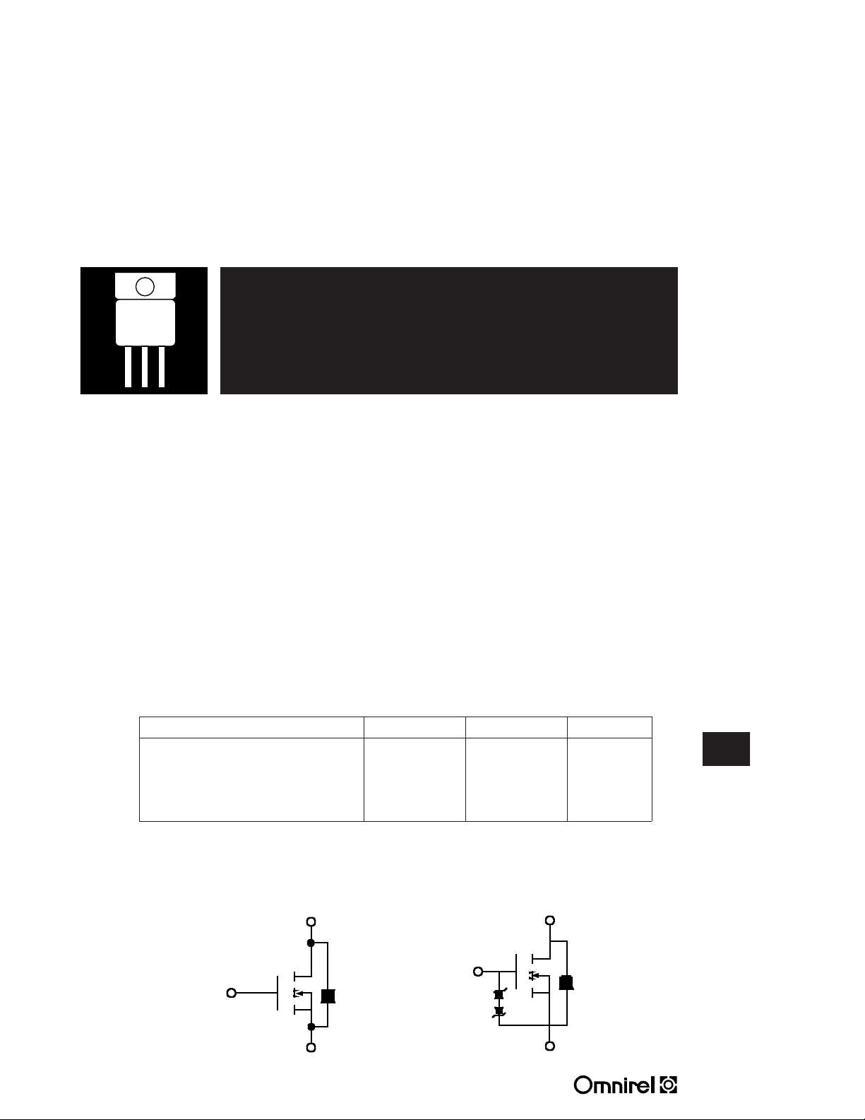
POWER MOSFET IN HERMETIC ISOLATED
JEDEC TO-258AA PACKAGE
100V Thru 500V, Up To 35 Amp, N-Channel
MOSFET With Or Without Zener Gate
Clamp Protection
FEATURES
• Isolated Hermetic Metal Package
• Bi-Lateral Zener Gate Protection (Optional)
• Fast Switching, Low Drive Current
• Ease Of Paralleling For Added Power
• Low R
• Available Screened To MIL-S-19500, TX, TXV And S Levels
DESCRIPTION
This series of hermetically packaged products feature the latest advanced MOSFET
and packaging technology. They are ideally suited for Military requirements where
small size, high performance and high reliability are required, and in applications such
as switching power supplies, motor controls, inverters, choppers, audio amplifiers and
high energy pulse circuits. The MOSFET gates are protected using bi-lateral zener
clamps in the OM6105SC series.
DS(on)
OM6107SC
OM6108SC
MAXIMUM RATINGS
Note: OM6105SC thru OM6108SC is supplied with zener gate protection.
4 11 R5
Supersedes 1 07 R4
PART NUMBER V
DS
R
DS(on)
I
D
OM6005SC/OM6105SC 100 V .065 35 A
OM6006SC/OM6106SC 200 V .095 30 A
OM6007SC/OM6107SC 400 V 0.3 15 A
OM6008SC/OM6108SC 500 V 0.4 13 A
OM6005SC thru OM6008SC is supplied without zener gate protection.
SCHEMATIC
WITHOUT ZENER CLAMPS WITH ZENER CLAMPS
OM6005SC - 6008SC OM6105SC - 6108SC
1 - DRAIN
3 - GATE
ZENERS
2 - SOURCE
3.1 - 75
1 - DRAIN
3 - GATE
2 - SOURCE
3.1
3.1
G
D
S
G
D
S
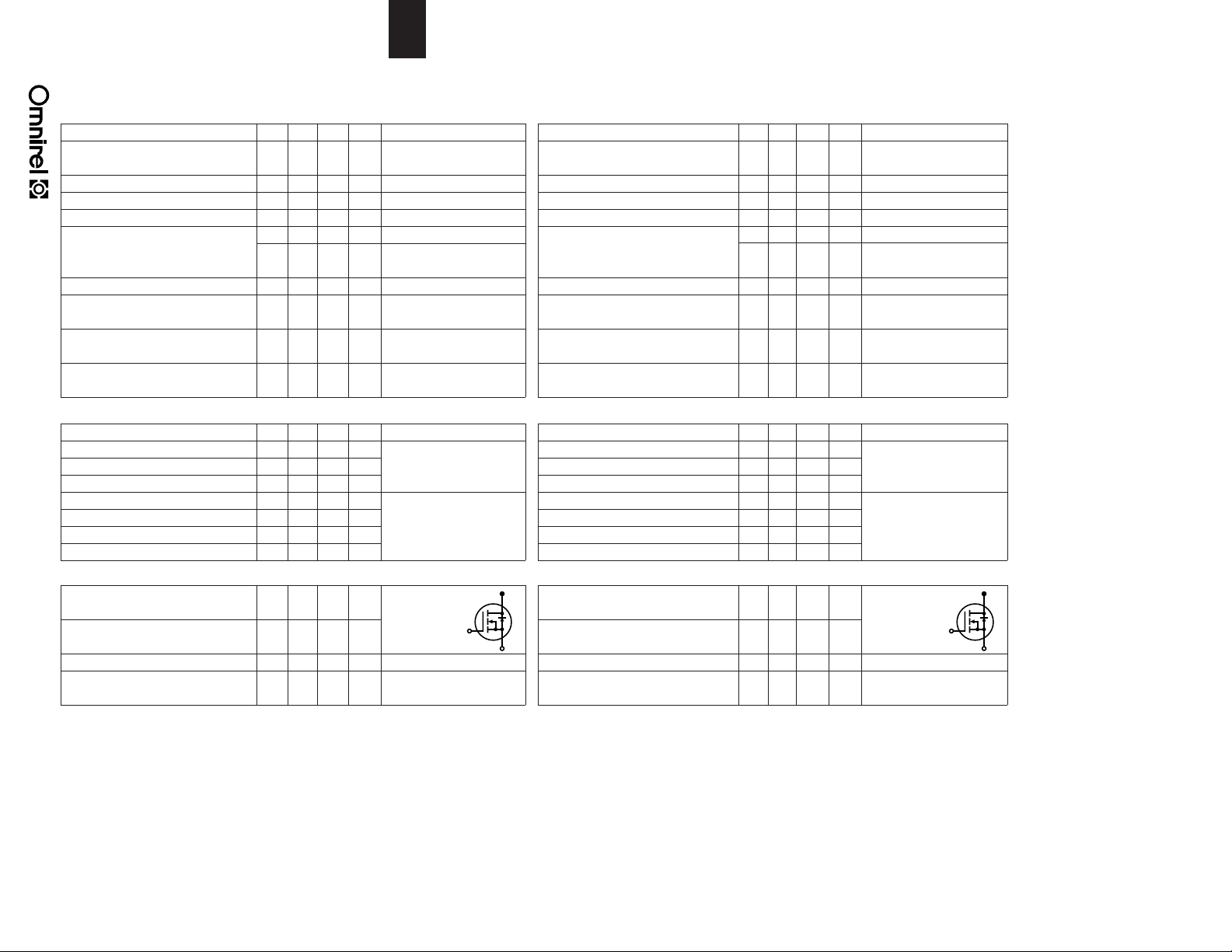
OM6005SC - OM6108SC
ELECTRICAL CHARACTERISTICS: (T
= 25°C unless otherwise noted) ELECTRICAL CHARACTERISTICS: (TC= 25°C unless otherwise noted)
C
STATIC P/N OM6105SC/OM6005SC (100V) STATIC P/N OM6106SC/OM6006SC (200V)
Parameter Min. Typ. Max. Units Test Conditions Parameter Min. Typ. Max. Units Test Conditions
BV
Drain-Source Breakdown
V
I
GSS
I
GSS
I
DSS
I
D(on)
V
R
R
3.1 - 76
DSS
Voltage I
Gate-Threshold Voltage 2.0 4.0 V VDS= VGS, ID= 250 mAV
GS(th)
Gate-Body Leakage (OM6105) ± 500 nA VGS= ± 12.8 V I
Gate-Body Leakage (OM6005) ± 100 nA VGS= ± 20 V I
Zero Gate Voltage Drain 0.1 0.25 mA VDS= Max. Rat., VGS= 0 I
Current
On-State Drain Current
Static Drain-Source On-State
DS(on)
DS(on)
DS(on)
1
Voltage
Static Drain-Source On-State
Resistance
1
Static Drain-Source On-State
Resistance
1
1
100 V
0.2 1.0 mA
35 A VDS 2 V
1.1 1.3 V V
0.55 0.65 V
.09 0.11
DYNAMIC DYNAMIC
g
Forward Transductance
fs
C
Input Capacitance 2700 pF VGS= 0 C
iss
C
Output Capacitance 1300 pF VDS= 25 V C
oss
C
Reverse Transfer Capacitance 470 pF f = 1 MHz C
rss
t
Turn-On Delay Time 28 ns VDD= 30 V, ID@ 20 A t
d(on)
t
Rise Time 45 ns Rg= 5.0 W, VG= 10V t
r
t
Turn-Off Delay Time 100 ns t
d(off)
t
Fall Time 50 ns t
f
1
9.0 10 S(W ) VDS 2 V
BODY-DRAIN DIODE RATINGS AND CHARACTERISTICS BODY-DRAIN DIODE RATINGS AND CHARACTERISTICS
I
Continuous Source Current
S
(Body Diode) symbol showing (Body Diode) symbol showing
I
SM
Source Current
1
(Body Diode) Junction rectifier. (Body Diode) Junction rectifier.
VSDDiode Forward Voltage
t
Reverse Recovery Time 400 ns
rr
1
1 Pulse Test: Pulse Width 300msec, Duty Cycle 2%. 1 Pulse Test: Pulse Width 300msec, Duty Cycle 2%.
- 40 A
- 160 A
- 2.5 V TC= 25 C, IS= -40 A, VGS= 0 VSDDiode Forward Voltage
VGS= 0, BV
= 250 mA Voltage ID= 250 mA
D
V
= 0.8 Max. Rat., VGS= 0, Current
DS
T
= 125° C TC= 125° C
C
GS
GS
, VGS= 10 V I
DS(on)
= 10 V, ID= 20 A
= 10 V, ID= 20 A
VGS= 10 V, ID= 20 A, R
TC= 125 C Resistance
(W )
Modified MOSPOWER I
the integral P-N I
T
J
dl
F
, ID= 20 A g
DS(on)
= 150 C, IF= IS,
/ds = 100 A/ms dlF/ds = 100 A/ms
Drain-Source Breakdown
DSS
Gate-Threshold Voltage 2.0 4.0 V VDS= VGS, ID= 250 mA
GS(th)
Gate-Body Leakage (OM6106) ± 500 nA VGS= ± 12.8 V
GSS
Gate-Body Leakage (OM6006) ± 100 nA VGS= ± 20 V
GSS
Zero Gate Voltage Drain 0.1 0.25 mA VDS= Max. Rat., VGS= 0
DSS
200 V
0.2 1.0 mA
On-State Drain Current
D(on)
V
Static Drain-Source On-State
DS(on)
R
DS(on)
DS(on)
fs
iss
oss
rss
d(on)
r
d(off)
f
S
SM
t
rr
1
Voltage
Static Drain-Source On-State
Resistance
1
Static Drain-Source On-State
1
Forward Transductance
Input Capacitance 2400 pF VGS= 0
Output Capacitance 600 pF VDS= 25 V
Reverse Transfer Capacitance 250 pF f = 1 MHz
Turn-On Delay Time 25 ns VDD= 75 V, ID@ 16 A
Rise Time 60 ns Rg= 5.0 W,VGS= 10V
Turn-Off Delay Time 85 ns
Fall Time 38 ns
Continuous Source Current
Source Current
Reverse Recovery Time 350 ns
1
30 A VDS 2 V
1.36 1.52 V V
.085 .095 V
0.14 0.17
1
10.0 12.5 S(W) VDS 2 V
(W )
- 30 A
1
1
- 120 A
- 2 V TC= 25 C, IS= -30 A, VGS= 0
VGS= 0,
VDS= 0.8 Max. Rat., VGS= 0,
, VGS= 10 V
DS(on)
= 10 V, ID= 16 A
GS
= 10 V, ID= 16 A
GS
VGS= 10 V, ID= 16 A,
TC= 125 C
, ID= 16 A
DS(on)
Modified MOSPOWER
the integral P-N
T
= 150 C, IF= IS,
J
 Loading...