


OM3957NMM OM3957STM
OM3957SMM
1.3 AMP LOW DROPOUT 3.3 FIXED VOLTAGE
REGULATOR APPROVED TO SMD 5962-98590
Three Terminal, 3.3 Volt Positive Fixed
Low Dropout Voltage Regulator In
Hermetic JEDEC TO-257AA
Please see mechanical
outlines herein
FEATURES
• Similar To Industry Standard LT1086 -3.3
• Approved To DS C C Standardized Military Drawing Number 5962-98590
• Built In Thermal Overload Protection
• Short Circuit Current Limiting
• A vailable In Isolated Package
• Output Voltage Tolerance is Guaranteed To ±1%
• Guaranteed Dropout Voltage At Multiple Current Levels
DESCRIPTION
and Surface Mount Packages
This 3.3 volt fixed voltage regulator is designed to provide 1.3A of current with a higher
efficiency than conventional voltage regulators. This device is designed to operate down to 1
volt input to output dif ferential and the 1.5V dropout voltage is guaranteed at the maximum
output current. This device is ideally suited for those systems where high reliability, small size
and low weight are required. The isolated package simplifies the system assembly methods.
ABSOLUTE MAXIMUM RATINGS @ 25°C
Input Vo ltage . . . . . . . . . . . . . . . . . . . . . . . . . . . . . . . . . . . . . . . . . . . . . . . . . .. . . . . . 30 V
Output Current . . . . . . . . . . . . . . . . . . . . . . . . . . . . . . . . . . . . . . . . . . . . . . . . . .. . . . . . 1.3 A
Operating Junction Te mperature . . . . . . . . . . . . . . . . . . . . . . . . . . . . . . . . . .- 65°C to + 150°C
Storage Te mperature Range . . . . . . . . . . . . . . . . . . . . . . . . . . . . . . . . . . . .- 65°C to + 150°C
Lead Temperature (Soldering 10 seconds) . . . . . . . . . . . . . . . . . . . . . . . . . . . . . . . . . . . 300°C
Power Dissipation (Pd) . . . . . . . . . . . . . . . . . . . . . . . . . . . . . . . . . . . . . . . . . Internally Limited
Thermal Resistance:
qJC(Isolated) . . . . . . . . . . . . . . . . . . . . . . . . . . . . . . . . . . . . . . . . . . . . . . . . . . . 4.2°C/W
qJA. . . . . . . . . . . . . . . . . . . . . . . . . . . . . . . . . . . . . . . . . . . . . . . . . . . . . . . . . . . 42°C/W
Part Number Designator
Standard Military Drawing Omnirel Part Number
5962-9859001MMA OM3957SMM
5962-9859001M U A OM3957STM
5962-9859001MNA OM3957NMM
9 01 R1
supersedes 8 07 R0
3.3 - 1
OM3957NMM OM3957STM
OM3957SMM
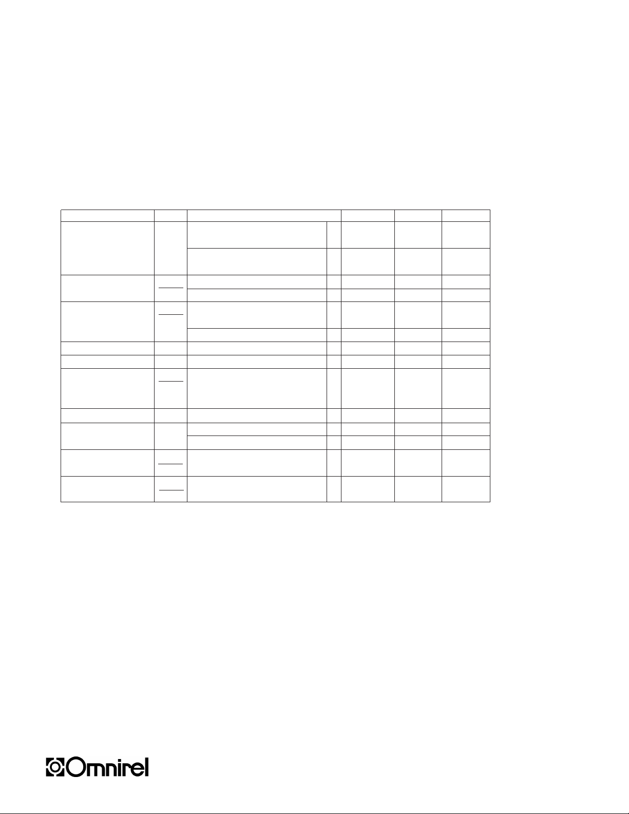
ELECTRICAL CHARACTERISTICS -55°C T
125°C (unless otherwise specified)
A
Parameter Symbol Test Conditions Min. Max. Unit
Output Voltage V
Line Regulation ³V
(Note 1) ³ V
Load Regulation ³V
(Note 1) ³I
Dropout Voltage V
OUT
OUT
IN
OUT
OUT
DO
Thermal Regulation - 30 m s pulse, T
Ripple Rejection ³V
Quiescent Current I
Current Limit I
Temperature Stability ³V
IN
³V
OUT
Q
Lim
OUT
VIN= 5.0 V, I
4.75 V V
10 mA I
4.5V VIN 18 V, I
4.5V VIN 18 V, I
VIN= 5.0 V, 0A I
= 10 mA 3.267 3.333 V
OUT
T
= 25° C
A
18 V, • 3.235 3.365 V
IN
1.3 A
OUT
= 0 A, TA= 25° C 10 m V
OUT
= 0 A • 12
OUT
1.3 A 15 m V
OUT
TA= 25° C
V
= 5.0 V, 0A I
IN
I
= 1.3 A, ³V
OUT
f = 120 Hz, C
C
= 25 µF (tantalum), I
OUT
V
IN
= 6.3 V
1.3 A • 25 m V
OUT
= 1% • 1.5 V
REF
= +25° C 0.04 % / W
A
= 25 µF, • 60 dB
Adj
= 1.3 A,
OUT
VIN= 18 V • 10 m A
V
= 8.3 V • 1.3 2.5 A
IN
= 28.3 V • .050 --A
V
IN
-55° C TJ +125° C 1 . 5 %
(Note 2) ³T
Long Term Stability ³V
OUT
TA= +125° C, t = 1000 hrs 1.0 %
(Note 2) ³T
Notes:
1. Line and Load Regulation are measured at a constant junction temperature using a low duty cycle pulse technique.
Although power dissipation is internally limited, regulation is guaranteed up to the maximum power dissipation of 13 W.
Power dissipation is determined by the input/output differential voltage and the output current. Guaranteed maximum
power dissipation will not be available over the full input/output voltage range.
2. Guaranteed by design, characterization or correlation to other tested parameters.
3. The • denotes the specifications which apply over the full operating temperature range.

205 Crawford Street, Leominster, MA 01453 USA (978) 534-5776 FAX (978) 537-4246
Visit Our Web Site at www.omnirel.com
.430
.410
.200
.190
.038 MAX.
.005
.120 TYP.
.537
.527
.665
.645
.420
.410
.150
.140
.750
.500
.100 TYP.
.035
.025
.045
.035
.425
.200
.100
.350 MIN.
.080
.160
.020
± .020
.035 WIDE
FLAT 3 PLCS.
.115
.425
OM3957STM
.450
.140
.415
.157
.015
.140
.140
.050
.050
.037
.375
.030
MIN.
.625
OM3957NMM OM3957STM
OM3957SMM
MECHANICAL OUTLINE
CONNECTION DIAGRAM
NOTES
• Case is metal/hermetically sealed
• Isolated Tab
OM3957SMM OM3957NMM
4
123
PIN OUT
1 Ground
2V
OUT
3V
IN
4 Isolated
MECHANICAL OUTLINE MECHANICAL OUTLINE
1
3
2
Front View
Pin 1 - Ground
Pin 2 - V
Pin 3 - V
Tab - Isolated
IN
OUT
Front View
Pin 1 - V
Pin 2 - Ground
Pin 3 - V
IN
OUT
12
3

THANK YOU FOR YOUR INTEREST
205 Crawford Street, Leominster, MA 01453 USA (978) 534-5776 FAX (978) 537-4246
Visit Our Web Site at www.omnirel.com
THANK YOU FOR YOUR INTEREST
IN OMNIREL
IN OMNIREL
’S PRODUCTS!
’S PRODUCTS!
 Loading...