


Motorola MC74LVX245D, MC74LVX245DT, MC74LVX245M Datasheet
SEMICONDUCTOR TECHNICAL DATA
1
REV 0
Motorola, Inc. 1997
6/97
The MC74LVX245 is an advanced high speed CMOS octal bus
transceiver.
It is intended for two–way asynchronous communication between data
buses. The direction of data transmission is determined by the level of the
T/R
input. The output enable pin (OE) can be used to disable the device,
so that the buses are effectively isolated.
All inputs are equipped with protection circuits against static discharge.
• High Speed: t
PD
= 4.7ns (Typ) at VCC = 3.3V
• Low Power Dissipation: I
CC
= 4µA (Max) at TA = 25°C
• Power Down Protection Provided on Inputs
• Balanced Propagation Delays
• Low Noise: V
OLP
= 0.8V (Max)
• Pin and Function Compatible with Other Standard Logic Families
• Latchup Performance Exceeds 300mA
• ESD Performance: HBM > 2000V; Machine Model > 200V
APPLICATION NOTES
1. Do not force a signal on an I/O pin when it is an active output, damage may
occur.
2. All floating (high impedence) input or I/O pins must be fixed by means of
pull up or pull down resistors or bus terminator ICs.
3. A parasitic diode is formed between the bus and VCC terminals. Therefore,
the LVX245 cannot be used to interface 5V to 3V systems directly.
Figure 1. 20–Lead Pinout (Top View)
1920 18 17 16 15 14
21 34567
V
CC
13
8
12
9
11
10
OE
B0 B1 B2 B3 B4 B5 B6 B7
T/R
A0 A1 A2 A3 A4 A5 A6 A7 GND
LVX
LOW–VOLTAGE CMOS
DW SUFFIX
20–LEAD SOIC PACKAGE
CASE 751D–04
DT SUFFIX
20–LEAD TSSOP PACKAGE
CASE 948E–02
M SUFFIX
20–LEAD SOIC EIAJ PACKAGE
CASE 967–01
PIN NAMES
Function
Output Enable Input
Transmit/Receive Input
Side A 3–State Inputs or 3–State
Outputs
Side B 3–State Inputs or 3–State
Outputs
Pins
OE
T/R
A0–A7
B0–B7
MC74LVX245
MOTOROLA LCX DATA
BR1339 — REV 3
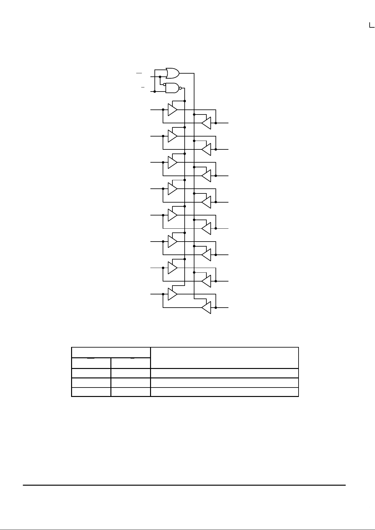
2
B0
OE
19
T/R 1
A0
B1
A1
B2
A2
B3
A3
B4
A4
B5
A5
B6
A6
B7
A7
Figure 2. Logic Diagram
2
3
4
5
6
7
8
9
18
17
16
15
14
13
12
11
INPUTS
OE T/R
OPERATING MODE
Non–Inverting
L L B Data to A Bus
L H A Data to B Bus
H X Z
H = High Voltage Level; L = Low V oltage Level; Z = High Impedance State; X = High or Low Voltage Level
and Transitions are Acceptable; For ICC reasons, Do Not Float Inputs
MC74LVX245
LCX DATA
BR1339 — REV 3
3 MOTOROLA
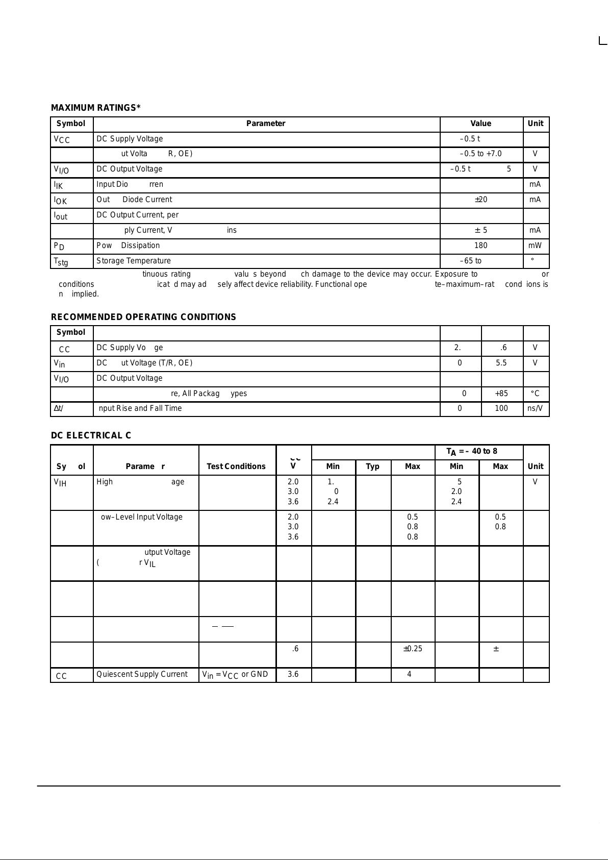
MAXIMUM RATINGS*
Symbol
Parameter
Value
Unit
V
CC
DC Supply Voltage
–0.5 to +7.0
V
V
in
DC Input Voltage (T/R, OE)
–0.5 to +7.0
V
V
I/O
DC Output Voltage
–0.5 to VCC +0.5
V
I
IK
Input Diode Current
–20
mA
I
OK
Output Diode Current
±20
mA
I
out
DC Output Current, per Pin
±25
mA
I
CC
DC Supply Current, VCC and GND Pins
±75
mA
P
D
Power Dissipation
180
mW
T
stg
Storage Temperature
–65 to +150
_
C
* Absolute maximum continuous ratings are those values beyond which damage to the device may occur. Exposure to these conditions or
conditions beyond those indicated may adversely affect device reliability. Functional operation under absolute–maximum–rated conditions is
not implied.
RECOMMENDED OPERATING CONDITIONS
Symbol
Parameter
Min
Max
Unit
V
CC
DC Supply Voltage
2.0
3.6
V
V
in
DC Input Voltage (T/R, OE)
0
5.5
V
V
I/O
DC Output Voltage
0
V
CC
V
T
A
Operating Temperature, All Package Types
–40
+85
_
C
∆t/∆V
Input Rise and Fall Time
0
100
ns/V
DC ELECTRICAL CHARACTERISTICS
ОООООО
V
TA = 25°C
TA = – 40 to 85°C
Symbol
Parameter
ОООООО
Test Conditions
V
CC
V
Min
Typ
Max
Min
Max
Unit
ÎÎ
Î
V
IH
ОООООО
Î
High–Level Input Voltage
ОООООО
ОООООÎÎ
Î
2.0
3.0
3.6
ÎÎ
Î
1.5
2.0
2.4
ÎÎÎÎÎÎÎ
Î
1.5
2.0
2.4
ÎÎÎÎ
V
ÎÎ
Î
V
IL
ОООООО
Î
Low–Level Input Voltage
ОООООО
ОООООÎÎ
Î
2.0
3.0
3.6
ÎÎÎÎÎÎÎ
Î
0.5
0.8
0.8
ÎÎÎÎÎ
Î
0.5
0.8
0.8
Î
V
ÎÎ
Î
ÎÎ
Î
V
OH
ОООООО
Î
ОООООО
Î
High–Level Output Voltage
(Vin = VIH or VIL)
ОООООО
ООООО
Î
ООООО
Î
IOH = –50µA
IOH = –50µA
IOH = –4mA
Î
Î
Î
Î
2.0
3.0
3.0
ÎÎ
Î
ÎÎ
Î
1.9
2.9
2.58
Î
Î
Î
Î
2.0
3.0
ÎÎ
Î
ÎÎ
Î
ÎÎ
Î
ÎÎ
Î
1.9
2.9
2.48
ÎÎ
Î
ÎÎ
Î
Î
Î
V
ÎÎ
Î
V
OL
ОООООО
Î
Low–Level Output Voltage
(Vin = VIH or VIL)
ОООООО
ООООО
Î
IOL = 50µA
IOL = 50µA
IOL = 4mA
Î
Î
2.0
3.0
3.0
ÎÎÎÎ
Î
0.0
0.0
ÎÎ
Î
0.1
0.1
0.36
ÎÎÎÎÎ
Î
0.1
0.1
0.44
Î
V
ÎÎ
Î
I
in
ОООООО
Î
Input Leakage Current
ОООООО
ООООО
Î
Vin = 5.5V or GND
(T/R
, OE)
Î
Î
3.6
ÎÎÎÎÎÎÎ
Î
±0.1
ÎÎÎÎÎ
Î
±1.0
Î
µA
I
OZ
Maximum Three–State
Leakage Current
ОООООО
Vin = VIL or V
IH
V
out
= VCC or GND
3.6
±0.25
±2.5
µA
I
CC
Quiescent Supply Current
ОООООО
Vin = VCC or GND
3.6
4.0
40.0
µA
 Loading...