


 Loading...
Mitsubishi M37560MF-XXXGP, M37560MF-XXXFP, M37560ME-XXXGP, M37560ME-XXXFP, M37560MD-XXXGP Datasheet
...MITSUBISHI MICROCOMPUTERS
7560 Group
SINGLE-CHIP 8-BIT CMOS MICROCOMPUTER
DESCRIPTION
The 7560 group is the 8-bit microcomputer based on the 740 family core technology.
The 7560 group has the LCD drive control circuit, an 8-channel A- D/D-A converter, UART and PWM as additional functions.
The various microcomputers in the 7560 group include variations of internal memory size and packaging. For details, refer to the section on part numbering.
For details on availability of microcomputers in the 7560 Group, refer the section on group expansion.
FEATURES |
|
• Basic machine-language instructions ....................................... |
71 |
• The minimum instruction execution time ............................ |
0.5 s |
(at 8 MHz oscillation frequency) |
|
• Memory size |
|
ROM ................................................................ |
32 K to 60 K bytes |
RAM ............................................................... |
1024 to 2560 bytes |
• Programmable input/output ports ............................................. |
55 |
• Software pull-up resistors .................................................... |
Built-in |
• Output ports ................................................................................. |
8 |
• Input ports .................................................................................... |
1 |
•Interrupts .................................................. |
17 sources, 16 vectors |
(includes key input interrupt) |
|
• Timers ........................................................... |
8-bit 3, 16-bit 2 |
• Serial I/O1 ..................... |
8-bit 1 (UART or Clock-synchronous) |
• Serial I/O2 .................................... |
8-bit 1 (Clock-synchronous) |
• PWM output .................................................................... |
8-bit 1 |
• A-D converter .................................................. |
8-bit 8 channels |
• D-A converter .................................................. |
8-bit 2 channels |
• LCD drive control circuit |
|
Bias ................................................................................... |
1/2, 1/3 |
Duty ............................................................................ |
1/2, 1/3, 1/4 |
Common output .......................................................................... |
4 |
Segment output ......................................................................... |
40 |
•2 Clock generating circuits
(connect to external ceramic resonator or quartz-crystal oscillator)
• Watchdog timer ............................................................. |
14-bit 1 |
• Power source voltage ................................................ |
2.2 to 5.5 V |
• Power dissipation |
|
In high-speed mode ........................................................... |
40 mW |
(at 8 MHz oscillation frequency, at 5 V power source voltage) |
|
In low-speed mode .............................................................. |
60 W |
(at 32 kHz oscillation frequency, at 3 V power source voltage) |
|
• Operating temperature range ................................... |
– 20 to 85°C |
APPLICATIONS
Camera, household appliances, consumer electronics, etc.
PIN CONFIGURATION (TOP VIEW)
|
|
|
|
|
|
|
|
|
SEG10 |
SEG11 |
SEG12 |
SEG13 |
SEG14 |
SEG15 |
SEG16 |
SEG17 |
P30/SEG18 |
P31/SEG19 P32/SEG20 P33/SEG21 P34/SEG22 P35/SEG23 P36/SEG24 P37/SEG25 P00/SEG26 P01/SEG27 P02/SEG28 P03/SEG29 P04/SEG30 P05/SEG31 P06/SEG32 P07/SEG33 |
P10/SEG34 |
P11/SEG35 P12/SEG36 P13/SEG37 |
P14/SEG38 |
P15/SEG39 |
|
|
|
|
|
|
||||||||||||||||||||||||||||||||||||||||||||||||||||||||||||||
|
|
|
|
|
|
|
|
|
|
|
|
|
|
|
|
|
|
|
|
|
|
|
|
|
|
|
|
|
|
|
|
|
|
|
|
|
|
|
|
|
|
|
|
|
|
|
|
|
|
|
|
|
|
|
|
|
|
|
|
|
|
|
|
|
|
|
|
|
|
|
|
|
|
|
|
|
|
|
|
|
|
|
|
|
|
|
|
|
|
|
|
|
|
|
|
|
|
|
|
|
|
|
|
|
|
|
|
|
|
|
|
|
|
|
|
|
|
|
|
|
|
|
|
|
|
|
|
|
|
|
|
|
|
|
|
|
|
|
|
|
|
|
|
|
|
|
|
|
|
|
|
|
|
|
|
|
|
|
|
|
|
|
|
|
|
|
|
|
|
|
|
|
|
|
|
|
|
|
|
|
|
|
|
|
|
|
|
|
|
|
|
|
|
|
|
|
|
|
|
|
|
|
|
|
|
|
|
|
|
|
|
|
|
|
|
|
|
|
|
|
|
|
|
|
|
|
|
|
|
|
|
|
|
|
|
|
|
|
|
|
|
|
|
|
|
|
|
|
|
|
|
|
|
|
|
|
|
|
|
|
|
|
|
|
|
|
|
|
|
|
|
|
|
|
|
|
|
|
|
|
|
80 |
79 |
78 |
77 |
76 |
75 |
74 |
73 |
72 |
71 |
70 |
69 |
68 |
67 |
66 |
65 |
64 |
63 |
|
62 |
61 |
60 |
59 |
58 57 |
56 |
55 |
54 |
53 |
52 |
51 |
|
|
|
|
|
|
|
|||||||||||||||||||||||||||||||||||||||||||||
|
|
|
|
|
|
|
|
|
|
|
|
|
|
|
|
|
|
|
|
|
|
|
|
|
|
|
|
|
|
|
|
|
|
|
|
|
|
|
|
|
|
|
|
|
|
|
|
|
|
|
|
|
|
|
|
|
|
|
|
|
|
|
|
|
|
|
|
|
|
|
|
|
|
|
|
|
|
|
|
|
|
|
|
|
|
|
|
|
|
|
SEG9 |
|
|
|
81 |
|
|
|
|
|
|
|
|
|
|
|
|
|
|
|
|
|
|
|
|
|
|
|
|
|
|
|
|
|
|
|
|
|
|
|
|
|
|
|
|
|
|
|
|
|
|
|
|
|
|
|
|
|
|
|
|
|
|
|
|
|
|
|
|
|
|
|
|
|
|
|
|
|
|
|
50 |
|
|
|
P16 |
||||||
|
|
|
|
|
|
|
|
|
|
|
|
|
|
|
|
|
|
|
|
|
|
|
|
|
|
|
|
|
|
|
|
|
|
|
|
|
|
|
|
|
|
|
|
|
|
|
|
|
|
|
|
|
|
|
|
|
|
|
|
|
|
|
|
|
|
|
|
|
|
|
|
|
|
|
|
|
|
|
|
|||||||||||
SEG8 |
|
|
|
82 |
|
|
|
|
|
|
|
|
|
|
|
|
|
|
|
|
|
|
|
|
|
|
|
|
|
|
|
|
|
|
|
|
|
|
|
|
|
|
|
|
|
|
|
|
|
|
|
|
|
|
|
|
|
|
|
|
|
|
|
|
|
|
|
|
|
|
|
|
|
|
|
|
|
|
|
49 |
|
|
|
P17 |
||||||
|
|
|
|
|
|
|
|
|
|
|
|
|
|
|
|
|
|
|
|
|
|
|
|
|
|
|
|
|
|
|
|
|
|
|
|
|
|
|
|
|
|
|
|
|
|
|
|
|
|
|
|
|
|
|
|
|
|
|
|
|
|
|
|
|
|
|
|
|
|
|
|
|
|
|
|
|
|
|
|
|||||||||||
SEG7 |
|
|
|
83 |
|
|
|
|
|
|
|
|
|
|
|
|
|
|
|
|
|
|
|
|
|
|
|
|
|
|
|
|
|
|
|
|
|
|
|
|
|
|
|
|
|
|
|
|
|
|
|
|
|
|
|
|
|
|
|
|
|
|
|
|
|
|
|
|
|
|
|
|
|
|
|
|
|
|
|
48 |
|
|
|
P20 |
||||||
|
|
|
|
|
|
|
|
|
|
|
|
|
|
|
|
|
|
|
|
|
|
|
|
|
|
|
|
|
|
|
|
|
|
|
|
|
|
|
|
|
|
|
|
|
|
|
|
|
|
|
|
|
|
|
|
|
|
|
|
|
|
|
|
|
|
|
|
|
|
|
|
|
|
|
|
|
|
|
|
|||||||||||
SEG6 |
|
|
|
84 |
|
|
|
|
|
|
|
|
|
|
|
|
|
|
|
|
|
|
|
|
|
|
|
|
|
|
|
|
|
|
|
|
|
|
|
|
|
|
|
|
|
|
|
|
|
|
|
|
|
|
|
|
|
|
|
|
|
|
|
|
|
|
|
|
|
|
|
|
|
|
|
|
|
|
|
47 |
|
|
|
P21 |
||||||
|
|
|
|
|
|
|
|
|
|
|
|
|
|
|
|
|
|
|
|
|
|
|
|
|
|
|
|
|
|
|
|
|
|
|
|
|
|
|
|
|
|
|
|
|
|
|
|
|
|
|
|
|
|
|
|
|
|
|
|
|
|
|
|
|
|
|
|
|
|
|
|
|
|
|
|
|
|
|
|
|||||||||||
SEG5 |
|
|
|
85 |
|
|
|
|
|
|
|
|
|
|
|
|
|
|
|
|
|
|
|
|
|
|
|
|
|
|
|
|
|
|
|
|
|
|
|
|
|
|
|
|
|
|
|
|
|
|
|
|
|
|
|
|
|
|
|
|
|
|
|
|
|
|
|
|
|
|
|
|
|
|
|
|
|
|
|
46 |
|
|
|
P22 |
||||||
|
|
|
|
|
|
|
|
|
|
|
|
|
|
|
|
|
|
|
|
|
|
|
|
|
|
|
|
|
|
|
|
|
|
|
|
|
|
|
|
|
|
|
|
|
|
|
|
|
|
|
|
|
|
|
|
|
|
|
|
|
|
|
|
|
|
|
|
|
|
|
|
|
|
|
|
|
|
|
|
|||||||||||
SEG4 |
|
|
|
86 |
|
|
|
|
|
|
|
|
|
|
|
|
|
|
|
|
|
|
|
|
|
|
|
|
|
|
|
|
|
|
|
|
|
|
|
|
|
|
|
|
|
|
|
|
|
|
|
|
|
|
|
|
|
|
|
|
|
|
|
|
|
|
|
|
|
|
|
|
|
|
|
|
|
|
|
45 |
|
|
|
P23 |
||||||
|
|
|
|
|
|
|
|
|
|
|
|
|
|
|
|
|
|
|
|
|
|
|
|
|
|
|
|
|
|
|
|
|
|
|
|
|
|
|
|
|
|
|
|
|
|
|
|
|
|
|
|
|
|
|
|
|
|
|
|
|
|
|
|
|
|
|
|
|
|
|
|
|
|
|
|
|
|
|
|
|||||||||||
SEG3 |
|
|
|
87 |
|
|
|
|
|
|
|
|
|
|
|
|
|
|
|
|
|
|
|
|
|
|
|
|
|
|
|
|
|
|
|
|
|
|
|
|
|
|
|
|
|
|
|
|
|
|
|
|
|
|
|
|
|
|
|
|
|
|
|
|
|
|
|
|
|
|
|
|
|
|
|
|
|
|
|
44 |
|
|
|
P24 |
||||||
|
|
|
|
|
|
|
|
|
|
|
|
|
|
|
|
|
|
|
|
|
|
|
|
|
|
|
|
|
|
|
|
|
|
|
|
|
|
|
|
|
|
|
|
|
|
|
|
|
|
|
|
|
|
|
|
|
|
|
|
|
|
|
|
|
|
|
|
|
|
|
|
|
|
|
|
|
|
|
|
|||||||||||
SEG2 |
|
|
|
88 |
|
|
|
|
|
|
|
|
|
|
|
|
|
|
|
|
|
|
|
|
|
|
|
|
|
|
|
|
|
|
|
|
|
|
|
|
|
|
|
|
|
|
|
|
|
|
|
|
|
|
|
|
|
|
|
|
|
|
|
|
|
|
|
|
|
|
|
|
|
|
|
|
|
|
|
43 |
|
|
|
P25 |
||||||
|
|
|
|
|
|
|
|
|
|
|
|
|
|
|
|
|
|
|
|
|
|
|
|
|
|
|
|
|
|
|
|
|
|
|
|
|
|
|
|
|
|
|
|
|
|
|
|
|
|
|
|
|
|
|
|
|
|
|
|
|
|
|
|
|
|
|
|
|
|
|
|
|
|
|
|
|
|
|
|
|||||||||||
SEG1 |
|
|
|
89 |
|
|
|
|
|
|
|
|
|
|
|
|
|
|
|
|
M37560MF-XXXFP |
|
|
|
|
|
|
|
|
|
|
|
|
42 |
|
|
|
P26 |
||||||||||||||||||||||||||||||||||||||||||||||||||||
|
|
|
|
|
|
|
|
|
|
|
|
|
|
|
|
|
|
|
|
|
|
|
|
|
|
|
|
|
|
|
|
|
|
|
||||||||||||||||||||||||||||||||||||||||||||||||||||||||
VCC |
91 |
|
|
|
|
|
|
|
|
|
|
|
|
|
|
|
|
|
|
|
|
|
|
|
|
|
|
|
|
40 |
|
|
|
VSS |
||||||||||||||||||||||||||||||||||||||||||||||||||||||||
SEG0 |
|
|
|
90 |
|
|
|
|
|
|
|
|
|
|
|
|
|
|
|
|
|
|
|
|
|
|
|
|
|
|
|
|
|
|
|
|
|
|
|
|
|
|
|
|
|
|
|
|
|
|
|
|
|
|
|
|
|
|
|
|
|
|
|
|
|
|
|
|
|
|
|
|
|
|
|
|
|
|
|
41 |
|
|
|
P27 |
||||||
|
|
|
|
|
|
|
|
|
|
|
|
|
|
|
|
|
|
|
|
|
|
|
|
|
|
|
|
|
|
|
|
|
|
|
|
|
|
|
|
|
|
|
|
|
|
|
|
|
|
|
|
|
|
|
|
|
|
|
|
|
|
|
|
|
|
|
|
|
|
|
|
|
|
|
|
|
|
|
|
|||||||||||
|
|
|
|
|
|
|
|
|
|
|
|
|
|
|
|
|
|
|
|
|
|
|
|
|
|
|
|
|
|
|
|
|
|
|
|
|
|
|
|
|
|
|
|
|
|
|
|
|
|
|
|
|
|
|
|
|
|
|
|
|
|
|
|
|
|
|
|
|
|
|
|
|
|
|
|
|
|
|
|
|
|
|
|
|
|
|
|
|
|
|
|
|
|
|
|
|
|
|
|
|
|
|
|
|
|
|
|
|
|
|
|
|
|
|
|
|
|
|
|
|
|
|
|
|
|
|
|
|
|
|
|
|
|
|
|
|
|
|
|
|
|
|
|
|
|
|
|
|
|
|
|
|
|
|
|
|
|
|
|
|
|
|
|
|
|
|
|
|
|
|
|
|
|
|
|
|
|
|
|
|
|
VREF |
|
|
|
92 |
|
|
|
|
|
|
|
|
|
|
|
|
|
|
|
|
|
|
|
|
|
|
|
|
|
|
|
|
|
|
|
|
|
|
|
|
|
|
|
|
|
|
|
|
|
|
|
|
|
|
|
|
|
|
|
|
|
|
|
|
|
|
|
|
|
|
|
|
|
|
|
|
|
|
|
39 |
|
|
|
XOUT |
||||||
|
|
|
|
|
|
|
|
|
|
|
|
|
|
|
|
|
|
|
|
|
|
|
|
|
|
|
|
|
|
|
|
|
|
|
|
|
|
|
|
|
|
|
|
|
|
|
|
|
|
|
|
|
|
|
|
|
|
|
|
|
|
|
|
|
|
|
|
|
|
|
|
|
|
|
|
|
|
|
||||||||||||
AVSS |
|
|
93 |
|
|
|
|
|
|
|
|
|
|
|
|
|
|
|
|
|
|
|
|
|
|
|
|
|
|
|
|
|
|
|
|
|
|
|
|
|
|
|
|
|
|
|
|
|
|
|
|
|
|
|
|
|
|
|
|
|
|
|
|
|
|
|
|
|
|
|
|
|
|
|
|
|
|
|
38 |
|
|
|
XIN |
|||||||
COM3 |
|
|
|
|
94 |
|
|
|
|
|
|
|
|
|
|
|
|
|
|
|
|
|
|
|
|
|
|
|
|
|
|
|
|
|
|
|
|
|
|
|
|
|
|
|
|
|
|
|
|
|
|
|
|
|
|
|
|
|
|
|
|
|
|
|
|
|
|
|
|
|
|
|
|
|
|
|
|
|
|
|
37 |
|
|
|
XCOUT |
|||||
|
|
|
|
|
|
|
|
|
|
|
|
|
|
|
|
|
|
|
|
|
|
|
|
|
|
|
|
|
|
|
|
|
|
|
|
|
|
|
|
|
|
|
|
|
|
|
|
|
|
|
|
|
|
|
|
|
|
|
|
|
|
|
|
|
|
|
|
|
|
|
|
|
|
|
|
|
|
|
|
|
|
|
||||||||
COM2 |
|
|
|
|
95 |
|
|
|
|
|
|
|
|
|
|
|
|
|
|
|
|
|
|
|
|
|
|
|
|
|
|
|
|
|
|
|
|
|
|
|
|
|
|
|
|
|
|
|
|
|
|
|
|
|
|
|
|
|
|
|
|
|
|
|
|
|
|
|
|
|
|
|
|
|
|
|
|
|
|
|
36 |
|
|
|
XCIN |
|||||
|
|
|
|
|
|
|
|
|
|
|
|
|
|
|
|
|
|
|
|
|
|
|
|
|
|
|
|
|
|
|
|
|
|
|
|
|
|
|
|
|
|
|
|
|
|
|
|
|
|
|
|
|
|
|
|
|
|
|
|
|
|
|
|
|
|
|
|
|
|
|
|
|
|
|
|
|
|
|
|
|
|
|
||||||||
COM1 |
|
|
|
|
96 |
|
|
|
|
|
|
|
|
|
|
|
|
|
|
|
|
|
|
|
|
|
|
|
|
|
|
|
|
|
|
|
|
|
|
|
|
|
|
|
|
|
|
|
|
|
|
|
|
|
|
|
|
|
|
|
|
|
|
|
|
|
|
|
|
|
|
|
|
|
|
|
|
|
|
|
35 |
|
|
|
|
|
|
|||
|
|
|
|
|
|
|
|
|
|
|
|
|
|
|
|
|
|
|
|
|
|
|
|
|
|
|
|
|
|
|
|
|
|
|
|
|
|
|
|
|
|
|
|
|
|
|
|
|
|
|
|
|
|
|
|
|
|
|
|
|
|
|
|
|
|
|
|
|
|
|
|
|
|
|
|
|
|
|
|
|
|
|
|
RESET |
||||||
COM0 |
|
|
|
97 |
|
|
|
|
|
|
|
|
|
|
|
|
|
|
|
|
|
|
|
|
|
|
|
|
|
|
|
|
|
|
|
|
|
|
|
|
|
|
|
|
|
|
|
|
|
|
|
|
|
|
|
|
|
|
|
|
|
|
|
|
|
|
|
|
|
|
|
|
|
|
|
|
|
|
|
34 |
|
|
|
|
P70/INT0 |
|||||
|
|
|
|
|
|
|
|
|
|
|
|
|
|
|
|
|
|
|
|
|
|
|
|
|
|
|
|
|
|
|
|
|
|
|
|
|
|
|
|
|
|
|
|
|
|
|
|
|
|
|
|
|
|
|
|
|
|
|
|
|
|
|
|
|
|
|
|
|
|
|
|
|
|
|
|
|
|
|
|
|||||||||||
VL3 |
|
|
|
98 |
|
|
|
|
|
|
|
|
|
|
|
|
|
|
|
|
|
|
|
|
|
|
|
|
|
|
|
|
|
|
|
|
|
|
|
|
|
|
|
|
|
|
|
|
|
|
|
|
|
|
|
|
|
|
|
|
|
|
|
|
|
|
|
|
|
|
|
|
|
|
|
|
|
|
|
33 |
|
|
|
|
P71 |
|||||
|
|
|
|
|
|
|
|
|
|
|
|
|
|
|
|
|
|
|
|
|
|
|
|
|
|
|
|
|
|
|
|
|
|
|
|
|
|
|
|
|
|
|
|
|
|
|
|
|
|
|
|
|
|
|
|
|
|
|
|
|
|
|
|
|
|
|
|
|
|
|
|
|
|
|
|
|
|
|
||||||||||||
VL2 |
|
|
99 |
|
|
|
|
|
|
|
|
|
|
|
|
|
|
|
|
|
|
|
|
|
|
|
|
|
|
|
|
|
|
|
|
|
|
|
|
|
|
|
|
|
|
|
|
|
|
|
|
|
|
|
|
|
|
|
|
|
|
|
|
|
|
|
|
|
|
|
|
|
|
|
|
|
|
|
32 |
|
|
|
|
P72 |
||||||
|
|
|
|
|
|
|
|
|
|
|
|
|
|
|
|
|
|
|
|
|
|
|
|
|
|
|
|
|
|
|
|
|
|
|
|
|
|
|
|
|
|
|
|
|
|
|
|
|
|
|
|
|
|
|
|
|
|
|
|
|
|
|
|
|
|
|
|
|
|
|
|
|
|
|
|
|
|
|
||||||||||||
C2 |
|
|
100 |
|
|
|
|
|
|
|
|
|
|
|
|
|
|
|
|
|
|
|
|
|
|
|
|
|
|
|
|
|
|
|
|
|
|
|
|
|
|
|
|
|
|
|
|
|
|
|
|
|
|
|
|
|
|
|
|
|
|
|
|
|
|
|
|
|
|
|
|
|
|
|
|
|
|
|
31 |
|
|
|
|
P73 |
||||||
|
|
|
|
|
|
|
|
|
1 |
|
2 |
|
3 |
|
4 |
|
5 |
|
6 |
|
7 |
|
8 |
|
9 |
|
|
10 |
11 |
12 |
13 |
14 |
15 |
16 |
17 |
18 |
|
19 |
20 |
21 |
22 |
23 |
24 |
25 |
26 |
27 |
28 |
29 |
30 |
|
|
|
|
|
|
|
||||||||||||||||||||||||||||||||||
|
|
|
|
|
|
|
|
|
|
|
|
|
|
|
|
|
|
|
|
|
|
|
|
|
|
|
|
|
|
|
|
|
|
|
|
|
|
|
|
|
|
|
|
|
|
|
|
|
|
|
|
|
|
|
|
|
|
|
|
|
|
|
|
|
|
|
|
|
|
|
|
|
|
|
|
|
|
|
|
|
|
|
|
|||||||
|
|
|
|
|
|
|
|
|
|
|
|
|
|
|
|
|
|
|
|
|
|
|
|
|
|
|
|
P60/SIN2/AN0 P57/ADT/DA2 P56/DA1 P55/CNTR1 P54/CNTR0 P53/RTP1 P52/RTP0 P51/PWM1 P50/PWM0 |
|
P47/SRDY1 P46/SCLK1 P45/TXD P44/RXD P43/φ /TOUT P42/INT2 |
P41/INT1 |
|
|
|
|
|
|
|
|
|
|
|
|
|
|
|
|
|
||||||||||||||||||||||||||||||||||||||||||
|
|
|
|
|
|
|
|
|
C1 |
VL1 |
P67/AN7 |
P66/AN6 |
P65/AN5 |
P64/AN4 |
P63/SCLK22/AN3 |
P62/SCLK21/AN2 |
P61/SOUT2/AN1 |
|
P40 P77 P76 |
P75 |
P74 |
|
|
|
|
|
|
|||||||||||||||||||||||||||||||||||||||||||||||||||||||||||||||
|
|
|
|
|
|
|
|
|
|
|
|
|
|
|
|
|||||||||||||||||||||||||||||||||||||||||||||||||||||||||||||||||||||||||||
|
|
|
|
|
|
|
|
|
|
|
|
|
|
|
|
|
|
|
|
|
|
|
|
|
|
|
|
|
|
|
||||||||||||||||||||||||||||||||||||||||||||||||||||||||||||
Package type : 100P6S-A
Fig. 1 Pin configuration of M37560MF-XXXFP
MITSUBISHI MICROCOMPUTERS
7560 Group
SINGLE-CHIP 8-BIT CMOS MICROCOMPUTER
PIN CONFIGURATION (TOP VIEW)
|
|
|
|
|
|
|
|
|
|
|
|
|
SEG13 |
|
SEG14 |
|
SEG15 |
|
SEG16 |
|
SEG17 |
|
P30/SEG18 |
|
P31/SEG19 |
|
P32/SEG20 |
|
P33/SEG21 |
|
P34/SEG22 P35/SEG23 P36/SEG24 P37/SEG25 P00/SEG26 P01/SEG27 P02/SEG28 P03/SEG29 P04/SEG30 P05/SEG31 P06/SEG32 P07/SEG33 |
|
P10/SEG34 P11/SEG35 P12/SEG36 |
|
P13/SEG37 |
|
|
|
|
|
|
|
||||||||||||||||||||||||||||||||||||||||||||
|
|
|
|
|
|
|
|
|
|
|
|
|
|
|
|
|
|
|
|
|
|
|
|
|
|
|
|
|
|
|
|
|
|
|
|
|
|
|
|
|
|
|
|
|
|
|
|
|
|
|
|
|
|
|
|
|
|
|
|
|
|
|
|
|
|
|
|
|
|
|
|
|
|
|
|
|
|
|
|
|
|
|
|
|
|
|
|
|
|
|
|
|
|
|
|
|
|
|
|
|
|
|
|
|
|
|
|
|
|
|
|
|
|
|
|
|
|
|
|
|
|
|
|
|
|
|
|
|
|
|
|
|
|
|
|
|
|
|
|
|
|
|
|
|
|
|
|
|
|
|
|
|
|
|
|
|
|
|
|
|
|
|
|
|
|
|
|
|
|
|
|
|
|
|
|
|
|
|
|
|
|
|
|
|
|
|
|
|
|
|
|
|
|
|
|
|
|
|
|
|
|
|
|
|
|
|
|
|
|
|
|
|
|
|
|
|
|
|
|
|
|
|
|
|
|
|
|
|
|
|
|
|
|
|
|
|
|
|
|
|
|
|
|
|
|
|
|
|
|
|
|
|
|
|
|
|
|
|
|
|
|
|
|
|
|
|
|
|
|
|
|
|
75 |
74 |
73 |
72 |
71 |
70 |
69 |
68 |
67 |
66 |
65 |
64 |
63 |
62 |
61 |
60 |
|
|
|
59 |
58 |
57 |
56 |
55 |
54 |
53 |
52 |
51 |
|
|
|
|
|
|
|
|
|||||||||||||||||||||||||||||||||||||||
SEG12 |
|
|
76 |
|
|
|
|
|
|
|
|
|
|
|
|
|
|
|
|
|
|
|
|
|
|
|
|
|
|
|
|
|
|
|
|
|
|
|
|
|
|
|
|
|
|
|
|
|
|
|
|
|
|
|
|
|
|
|
|
|
|
|
|
|
|
|
|
|
|
|
|
50 |
|
|
|
|
P14/SEG38 |
|||||||||
|
|
|
|
|
|
|
|
|
|
|
|
|
|
|
|
|
|
|
|
|
|
|
|
|
|
|
|
|
|
|
|
|
|
|
|
|
|
|
|
|
|
|
|
|
|
|
|
|
|
|
|
|
|
|
|
|
|
|
|
|
|
|
|
|
|
|
|
|
|
|
|
|
||||||||||||||
SEG11 |
|
|
|
|
|
|
|
|
|
|
|
|
|
|
|
|
|
|
|
|
|
|
|
|
|
|
|
|
|
|
|
|
|
|
|
|
|
|
|
|
|
|
|
|
|
|
|
|
|
|
|
|
|
|
|
|
|
|
|
|
|
|
|
|
|
|
|
|
|
|
|
|
|
|
|
|
|
|
|
|
||||||
|
|
77 |
|
|
|
|
|
|
|
|
|
|
|
|
|
|
|
|
|
|
|
|
|
|
|
|
|
|
|
|
|
|
|
|
|
|
|
|
|
|
|
|
|
|
|
|
|
|
|
|
|
|
|
|
|
|
|
|
|
|
|
|
|
|
|
|
|
|
|
|
49 |
|
|
|
|
P15/SEG39 |
||||||||||
SEG10 |
|
|
|
|
|
|
|
|
|
|
|
|
|
|
|
|
|
|
|
|
|
|
|
|
|
|
|
|
|
|
|
|
|
|
|
|
|
|
|
|
|
|
|
|
|
|
|
|
|
|
|
|
|
|
|
|
|
|
|
|
|
|
|
|
|
|
|
|
|
|
|
|
|
|
|
|
|
P16 |
||||||||
|
|
78 |
|
|
|
|
|
|
|
|
|
|
|
|
|
|
|
|
|
|
|
|
|
|
|
|
|
|
|
|
|
|
|
|
|
|
|
|
|
|
|
|
|
|
|
|
|
|
|
|
|
|
|
|
|
|
|
|
|
|
|
|
|
|
|
|
|
|
|
|
48 |
|
|
|
|
|||||||||||
SEG9 |
|
|
|
|
|
|
|
|
|
|
|
|
|
|
|
|
|
|
|
|
|
|
|
|
|
|
|
|
|
|
|
|
|
|
|
|
|
|
|
|
|
|
|
|
|
|
|
|
|
|
|
|
|
|
|
|
|
|
|
|
|
|
|
|
|
|
|
|
|
|
|
|
|
|
|
|
|
P17 |
||||||||
|
|
79 |
|
|
|
|
|
|
|
|
|
|
|
|
|
|
|
|
|
|
|
|
|
|
|
|
|
|
|
|
|
|
|
|
|
|
|
|
|
|
|
|
|
|
|
|
|
|
|
|
|
|
|
|
|
|
|
|
|
|
|
|
|
|
|
|
|
|
|
|
47 |
|
|
|
|
|||||||||||
SEG8 |
|
|
|
|
|
|
|
|
|
|
|
|
|
|
|
|
|
|
|
|
|
|
|
|
|
|
|
|
|
|
|
|
|
|
|
|
|
|
|
|
|
|
|
|
|
|
|
|
|
|
|
|
|
|
|
|
|
|
|
|
|
|
|
|
|
|
|
|
|
|
|
|
|
|
|
|
|
P20 |
||||||||
|
|
80 |
|
|
|
|
|
|
|
|
|
|
|
|
|
|
|
|
|
|
|
|
|
|
|
|
|
|
|
|
|
|
|
|
|
|
|
|
|
|
|
|
|
|
|
|
|
|
|
|
|
|
|
|
|
|
|
|
|
|
|
|
|
|
|
|
|
|
|
|
46 |
|
|
|
|
|||||||||||
SEG7 |
|
|
|
|
|
|
|
|
|
|
|
|
|
|
|
|
|
|
|
|
|
|
|
|
|
|
|
|
|
|
|
|
|
|
|
|
|
|
|
|
|
|
|
|
|
|
|
|
|
|
|
|
|
|
|
|
|
|
|
|
|
|
|
|
|
|
|
|
|
|
|
|
|
|
|
|
|
P21 |
||||||||
|
|
81 |
|
|
|
|
|
|
|
|
|
|
|
|
|
|
|
|
|
|
|
|
|
|
|
|
|
|
|
|
|
|
|
|
|
|
|
|
|
|
|
|
|
|
|
|
|
|
|
|
|
|
|
|
|
|
|
|
|
|
|
|
|
|
|
|
|
|
|
|
45 |
|
|
|
|
|||||||||||
SEG6 |
|
|
|
|
|
|
|
|
|
|
|
|
|
|
|
|
|
|
|
|
|
|
|
|
|
|
|
|
|
|
|
|
|
|
|
|
|
|
|
|
|
|
|
|
|
|
|
|
|
|
|
|
|
|
|
|
|
|
|
|
|
|
|
|
|
|
|
|
|
|
|
|
|
|
|
|
|
P22 |
||||||||
|
|
82 |
|
|
|
|
|
|
|
|
|
|
|
|
|
|
|
|
|
|
|
|
|
|
|
|
|
|
|
|
|
|
|
|
|
|
|
|
|
|
|
|
|
|
|
|
|
|
|
|
|
|
|
|
|
|
|
|
|
|
|
|
|
|
|
|
|
|
|
|
44 |
|
|
|
|
|||||||||||
SEG5 |
|
|
|
|
|
|
|
|
|
|
|
|
|
|
|
|
|
|
|
|
|
|
|
|
|
|
|
|
|
|
|
|
|
|
|
|
|
|
|
|
|
|
|
|
|
|
|
|
|
|
|
|
|
|
|
|
|
|
|
|
|
|
|
|
|
|
|
|
|
|
|
|
|
|
|
|
|
P23 |
||||||||
|
|
83 |
|
|
|
|
|
|
|
|
|
|
|
|
|
|
|
|
|
|
|
|
|
|
|
|
|
|
|
|
|
|
|
|
|
|
|
|
|
|
|
|
|
|
|
|
|
|
|
|
|
|
|
|
|
|
|
|
|
|
|
|
|
|
|
|
|
|
|
|
43 |
|
|
|
|
|||||||||||
SEG4 |
|
|
|
|
|
|
|
|
|
|
|
|
|
|
|
|
|
|
|
|
|
|
|
|
|
|
|
|
|
|
|
|
|
|
|
|
|
|
|
|
|
|
|
|
|
|
|
|
|
|
|
|
|
|
|
|
|
|
|
|
|
|
|
|
|
|
|
|
|
|
|
|
|
|
|
|
|
P24 |
||||||||
|
|
84 |
|
|
|
|
|
|
|
|
|
|
|
|
|
|
|
|
|
|
|
|
|
|
|
|
|
|
|
|
|
|
|
|
|
|
|
|
|
|
|
|
|
|
|
|
|
|
|
|
|
|
|
|
|
|
|
|
|
|
|
|
|
|
|
|
|
|
|
|
42 |
|
|
|
|
|||||||||||
SEG3 |
|
|
|
|
|
|
|
|
|
|
|
|
|
|
|
|
|
|
|
|
|
|
|
|
|
|
|
|
|
|
|
|
|
|
|
|
|
|
|
|
|
|
|
|
|
|
|
|
|
|
|
|
|
|
|
|
|
|
|
|
|
|
|
|
|
|
|
|
|
|
|
|
|
|
|
|
|
P25 |
||||||||
|
|
85 |
|
|
|
|
|
|
|
|
|
|
|
|
|
|
|
|
|
|
|
|
|
|
|
|
|
|
|
|
|
|
|
|
|
|
|
|
|
|
|
|
|
|
|
|
|
|
|
|
|
|
|
|
|
|
|
|
|
|
|
|
|
|
|
|
|
|
|
|
41 |
|
|
|
|
|||||||||||
SEG2 |
|
|
|
|
|
|
|
|
|
|
|
|
|
|
|
|
|
|
|
|
|
|
|
|
|
|
|
|
|
|
|
|
|
|
|
|
|
|
|
|
|
|
|
|
|
|
|
|
|
|
|
|
|
|
|
|
|
|
|
|
|
|
|
|
|
|
|
|
|
|
|
|
|
|
|
|
|
P26 |
||||||||
|
|
86 |
|
|
|
|
|
|
|
|
|
|
|
|
|
|
|
|
|
|
|
|
|
|
|
|
|
|
|
|
|
|
|
|
|
|
|
|
|
|
|
|
|
|
|
|
|
|
|
|
|
|
|
|
|
|
|
|
|
|
|
|
|
|
|
|
|
|
|
|
40 |
|
|
|
|
|||||||||||
SEG1 |
|
|
|
|
|
|
|
|
|
|
|
|
|
|
|
|
|
|
|
|
|
|
|
|
|
|
|
|
|
|
|
|
|
|
|
|
|
|
|
|
|
|
|
|
|
|
|
|
|
|
|
|
|
|
|
|
|
|
|
|
|
|
|
|
|
|
|
|
|
|
|
|
|
|
|
|
|
P27 |
||||||||
|
|
87 |
|
|
|
|
|
|
|
|
|
M37560MF-XXXGP |
|
|
|
|
|
|
|
|
|
|
|
|
|
|
|
39 |
|
|
|
|
||||||||||||||||||||||||||||||||||||||||||||||||||||||
|
|
|
|
|
|
|
|
|
|
|
|
|
|
|
|
|
|
|
|
|
|
|
|
|
|
|
|
|
|
|
|
|
|
|
|
|
|
|
|
XOUT |
||||||||||||||||||||||||||||||||||||||||||||||
VCC |
|
|
89 |
|
|
|
|
|
|
|
|
|
|
|
|
|
|
|
|
|
|
|
|
|
|
|
|
37 |
|
|
|
|
||||||||||||||||||||||||||||||||||||||||||||||||||||||
SEG0 |
|
|
88 |
|
|
|
|
|
|
|
|
|
|
|
|
|
|
|
|
|
|
|
|
|
|
|
|
|
|
|
|
|
|
|
|
|
|
|
|
|
|
|
|
|
|
|
|
|
|
|
|
|
|
|
|
|
|
|
|
|
|
|
|
|
|
|
|
|
|
|
|
38 |
|
|
|
|
VSS |
|||||||||
VREF |
|
|
|
|
|
|
|
|
|
|
|
|
|
|
|
|
|
|
|
|
|
|
|
|
|
|
|
|
|
|
|
|
|
|
|
|
|
|
|
|
|
|
|
|
|
|
|
|
|
|
|
|
|
|
|
|
|
|
|
|
|
|
|
|
|
|
|
|
|
|
|
|
|
|
|
|
|
|
|
|
|
XIN |
||||
|
|
|
|
|
|
|
|
|
|
|
|
|
|
|
|
|
|
|
|
|
|
|
|
|
|
|
|
|
|
|
|
|
|
|
|
|
|
|
|
|
|
|
|
|
|
|
|
|
|
|
|
|
|
|
|
|
|
|
|
|
|
|
|
|
|
|
|
|
|
|
|
|
|
|
|
|
|
|
|
|
||||||
|
|
|
|
|
|
|
|
|
|
|
|
|
|
|
|
|
|
|
|
|
|
|
|
|
|
|
|
|
|
|
|
|
|
|
|
|
|
|
|
|
|
|
|
|
|
|
|
|
|
|
|
|
|
|
|
|
|
|
|
|
|
|
|
|
|
|
|
|
|
|
|
|
|
|
|
|
||||||||||
|
|
|
90 |
|
|
|
|
|
|
|
|
|
|
|
|
|
|
|
|
|
|
|
|
|
|
|
|
|
|
|
|
|
|
|
|
|
|
|
|
|
|
|
|
|
|
|
|
|
|
|
|
|
|
|
|
|
|
|
|
|
|
|
|
|
|
|
|
|
|
|
|
36 |
|
|
|
|
||||||||||
AVSS |
|
|
|
|
|
|
|
|
|
|
|
|
|
|
|
|
|
|
|
|
|
|
|
|
|
|
|
|
|
|
|
|
|
|
|
|
|
|
|
|
|
|
|
|
|
|
|
|
|
|
|
|
|
|
|
|
|
|
|
|
|
|
|
|
|
|
|
|
|
|
|
|
|
|
|
|
|
XCOUT |
||||||||
|
|
|
91 |
|
|
|
|
|
|
|
|
|
|
|
|
|
|
|
|
|
|
|
|
|
|
|
|
|
|
|
|
|
|
|
|
|
|
|
|
|
|
|
|
|
|
|
|
|
|
|
|
|
|
|
|
|
|
|
|
|
|
|
|
|
|
|
|
|
|
|
|
35 |
|
|
|
|
||||||||||
COM3 |
|
|
|
|
|
|
|
|
|
|
|
|
|
|
|
|
|
|
|
|
|
|
|
|
|
|
|
|
|
|
|
|
|
|
|
|
|
|
|
|
|
|
|
|
|
|
|
|
|
|
|
|
|
|
|
|
|
|
|
|
|
|
|
|
|
|
|
|
|
|
|
|
|
|
|
|
|
XCIN |
||||||||
|
|
|
92 |
|
|
|
|
|
|
|
|
|
|
|
|
|
|
|
|
|
|
|
|
|
|
|
|
|
|
|
|
|
|
|
|
|
|
|
|
|
|
|
|
|
|
|
|
|
|
|
|
|
|
|
|
|
|
|
|
|
|
|
|
|
|
|
|
|
|
|
|
34 |
|
|
|
|
||||||||||
COM2 |
|
|
|
|
|
|
|
|
|
|
|
|
|
|
|
|
|
|
|
|
|
|
|
|
|
|
|
|
|
|
|
|
|
|
|
|
|
|
|
|
|
|
|
|
|
|
|
|
|
|
|
|
|
|
|
|
|
|
|
|
|
|
|
|
|
|
|
|
|
|
|
|
|
|
|
|
|
|
|
|
||||||
|
93 |
|
|
|
|
|
|
|
|
|
|
|
|
|
|
|
|
|
|
|
|
|
|
|
|
|
|
|
|
|
|
|
|
|
|
|
|
|
|
|
|
|
|
|
|
|
|
|
|
|
|
|
|
|
|
|
|
|
|
|
|
|
|
|
|
|
|
|
|
33 |
|
|
|
|
RESET |
|||||||||||
|
|
|
|
|
|
|
|
|
|
|
|
|
|
|
|
|
|
|
|
|
|
|
|
|
|
|
|
|
|
|
|
|
|
|
|
|
|
|
|
|
|
|
|
|
|
|
|
|
|
|
|
|
|
|
|
|
|
|
|
|
|
|
|
|
|
|
|
|
|
|
|
|
|
|
||||||||||||
COM1 |
|
|
|
|
|
|
|
|
|
|
|
|
|
|
|
|
|
|
|
|
|
|
|
|
|
|
|
|
|
|
|
|
|
|
|
|
|
|
|
|
|
|
|
|
|
|
|
|
|
|
|
|
|
|
|
|
|
|
|
|
|
|
|
|
|
|
|
|
|
|
|
|
|
|
|
|
|
P70/INT0 |
||||||||
|
|
|
94 |
|
|
|
|
|
|
|
|
|
|
|
|
|
|
|
|
|
|
|
|
|
|
|
|
|
|
|
|
|
|
|
|
|
|
|
|
|
|
|
|
|
|
|
|
|
|
|
|
|
|
|
|
|
|
|
|
|
|
|
|
|
|
|
|
|
|
|
|
32 |
|
|
|
|
||||||||||
COM0 |
|
|
|
|
|
|
|
|
|
|
|
|
|
|
|
|
|
|
|
|
|
|
|
|
|
|
|
|
|
|
|
|
|
|
|
|
|
|
|
|
|
|
|
|
|
|
|
|
|
|
|
|
|
|
|
|
|
|
|
|
|
|
|
|
|
|
|
|
|
|
|
|
|
|
|
|
|
|
|
P71 |
||||||
|
|
|
|
|
95 |
|
|
|
|
|
|
|
|
|
|
|
|
|
|
|
|
|
|
|
|
|
|
|
|
|
|
|
|
|
|
|
|
|
|
|
|
|
|
|
|
|
|
|
|
|
|
|
|
|
|
|
|
|
|
|
|
|
|
|
|
|
|
|
|
|
|
|
|
31 |
|
|
|
|
||||||||
|
|
|
|
|
|
|
|
|
|
|
|
|
|
|
|
|
|
|
|
|
|
|
|
|
|
|
|
|
|
|
|
|
|
|
|
|
|
|
|
|
|
|
|
|
|
|
|
|
|
|
|
|
|
|
|
|
|
|
|
|
|
|
|
|
|
|
|
|
|
|
|
|||||||||||||||
VL3 |
|
|
|
|
|
|
|
|
|
|
|
|
|
|
|
|
|
|
|
|
|
|
|
|
|
|
|
|
|
|
|
|
|
|
|
|
|
|
|
|
|
|
|
|
|
|
|
|
|
|
|
|
|
|
|
|
|
|
|
|
|
|
|
|
|
|
|
|
|
|
|
|
|
|
|
|
|
|
|
|
|
|
P72 |
|||
|
|
|
|
|
|
|
|
96 |
|
|
|
|
|
|
|
|
|
|
|
|
|
|
|
|
|
|
|
|
|
|
|
|
|
|
|
|
|
|
|
|
|
|
|
|
|
|
|
|
|
|
|
|
|
|
|
|
|
|
|
|
|
|
|
|
|
|
|
|
|
|
|
|
|
|
|
|
30 |
|
|
|
|
|||||
|
|
|
|
|
|
|
|
|
|
|
|
|
|
|
|
|
|
|
|
|
|
|
|
|
|
|
|
|
|
|
|
|
|
|
|
|
|
|
|
|
|
|
|
|
|
|
|
|
|
|
|
|
|
|
|
|
|
|
|
|
|
|
|
|
|
|
|
|
|
|
|
|
|
|
|
|
|
|
|
|
|
|
|
P73 |
||
VL2 |
|
|
|
|
|
|
|
|
97 |
|
|
|
|
|
|
|
|
|
|
|
|
|
|
|
|
|
|
|
|
|
|
|
|
|
|
|
|
|
|
|
|
|
|
|
|
|
|
|
|
|
|
|
|
|
|
|
|
|
|
|
|
|
|
|
|
|
|
|
|
|
|
|
|
|
|
|
|
29 |
|
|
|
|
||||
C2 |
|
|
|
|
|
|
|
|
|
|
|
|
|
|
|
|
|
|
|
|
|
|
|
|
|
|
|
|
|
|
|
|
|
|
|
|
|
|
|
|
|
|
|
|
|
|
|
|
|
|
|
|
|
|
|
|
|
|
|
|
|
|
|
|
|
|
|
|
|
|
|
|
|
|
|
|
|
|
|
|
P74 |
|||||
|
|
98 |
|
|
|
|
|
|
|
|
|
|
|
|
|
|
|
|
|
|
|
|
|
|
|
|
|
|
|
|
|
|
|
|
|
|
|
|
|
|
|
|
|
|
|
|
|
|
|
|
|
|
|
|
|
|
|
|
|
|
|
|
|
|
|
|
|
|
|
|
28 |
|
|
|
|
|||||||||||
C1 |
|
|
|
|
|
|
|
|
|
|
|
|
|
|
|
|
|
|
|
|
|
|
|
|
|
|
|
|
|
|
|
|
|
|
|
|
|
|
|
|
|
|
|
|
|
|
|
|
|
|
|
|
|
|
|
|
|
|
|
|
|
|
|
|
|
|
|
|
|
|
|
|
|
|
|
|
|
|
|
|
|
|
|
P75 |
||
|
|
99 |
|
|
|
|
|
|
|
|
|
|
|
|
|
|
|
|
|
|
|
|
|
|
|
|
|
|
|
|
|
|
|
|
|
|
|
|
|
|
|
|
|
|
|
|
|
|
|
|
|
|
|
|
|
|
|
|
|
|
|
|
|
|
|
|
|
|
|
|
27 |
|
|
|
|
|||||||||||
|
|
|
|
|
|
|
|
|
|
|
|
|
|
|
|
|
|
|
|
|
|
|
|
|
|
|
|
|
|
|
|
|
|
|
|
|
|
|
|
|
|
|
|
|
|
|
|
|
|
|
|
|
|
|
|
|
|
|
|
|
|
|
|
|
|
|
|
|
|
|
|
|
|
|
|
|
|
|
|
|
|
|
|
P76 |
||
VL1 |
|
|
100 |
|
|
|
|
|
|
|
|
|
|
|
|
|
|
|
|
|
|
|
|
|
|
|
|
|
|
|
|
|
|
|
|
|
|
|
|
|
|
|
|
|
|
|
|
|
|
|
|
|
|
|
|
|
|
|
|
|
|
|
|
|
|
|
|
|
|
|
|
26 |
|
|
|
|
||||||||||
|
|
|
|
|
|
|
|
|
|
|
|
1 |
|
2 |
|
3 |
|
4 |
|
5 |
|
6 |
|
7 |
|
8 |
|
9 |
|
10 |
|
11 |
12 |
13 |
14 |
15 |
|
16 |
|
|
17 |
|
18 |
19 |
20 |
21 |
22 |
23 |
24 |
25 |
|
|
|
|
|
|
|
|
||||||||||||||||||||||||||||
|
|
|
|
|
|
|
|
|
|
|
|
|
|
|
|
|
|
|
|
|
|
|
|
|
|
|
|
|
|
|
|
|
|
|
|
|
|
|
|
|
|
|
|
|
|
|
|
|
|
|
|
|
|
|
|
|
|
|
|
|
|
|
|
|
|
|
|
|
|
|
|
|
|
|||||||||||||
|
|
|
|
|
|
|
|
|
|
|
|
|
|
|
|
|
|
|
|
|
|
|
|
|
|
|
|
|
|
|
|
|
|
|
|
|
|
|
|
|
|
|
|
|
|
|
|
|
|
|
|
|
|
|
|
|
|
|
|
|
|
|
|
|
|
|
|
|
|
|
|
|
|
|
|
|
|
|
|
|
|
|
|
|
|
|
|
|
|
|
|
|
|
|
|
|
|
|
|
|
|
|
|
|
|
|
|
|
|
|
|
|
|
|
|
|
|
|
|
|
|
|
|
|
|
|
|
|
|
||||||||||||||||||||||||||||||||||||||||||||
|
|
|
|
|
|
|
|
|
|
|
|
P67/AN7 |
P66/AN6 |
P65/AN5 |
P64/AN4 |
P63/SCLK22/AN3 |
P62/SCLK21/AN2 |
P61/SOUT2/AN1 |
P60/SIN2/AN0 |
P57/ADT/DA2 |
P56/DA1 P55/CNTR1 P54/CNTR0 P53/RTP1 P52/RTP0 P51/PWM1 P50/PWM0 |
|
P47/SRDY1 P46/SCLK1 P45/TXD P44/RXD P43/φ /TOUT |
P42/INT2 P41/INT1 P40 |
P77 |
|
|
|
|
|
|
|
||||||||||||||||||||||||||||||||||||||||||||||||||||||
|
|
|
|
|
|
|
|
|
|
|
|
|
|
|
|
|
|
|
|
|
|
|
|
|
||||||||||||||||||||||||||||||||||||||||||||||||||||||||||||||
Package type : 100P6Q-A
Fig. 2 Pin configuration of M37560MF-XXXGP
2

MITSUBISHI MICROCOMPUTERS
7560 Group
SINGLE-CHIP 8-BIT CMOS MICROCOMPUTER
FUNCTIONAL BLOCK DIAGRAM (Package : 100P6S-A)
( 5 V ) ( 0 V )
Reset input
Clock |
output |
Clock |
input |
VSS
VCC
RESET
XOUT
XIN
VL1 |
C1 |
C2 |
VL2 |
VL3 |
2 |
1 |
100 |
99 |
98 |
40
Data bus
91
35
38 39 |
Clockgenerating circuit |
COM0 |
COM1 |
COM2 |
COM3 |
SEG0 |
SEG1 |
SEG2 |
SEG3 |
SEG4 |
SEG5 |
SEG6 |
SEG7 |
SEG8 |
SEG9 |
SEG10 |
SEG11 |
SEG12 |
SEG13 |
SEG14 |
SEG15 |
SEG16 |
SEG17 |
|
|
97 |
96 |
95 |
94 |
90 |
89 |
88 |
87 |
86 |
85 |
84 |
83 |
82 |
81 |
80 |
79 |
78 |
77 |
76 |
75 |
74 |
73 |
|
|
|
|
|
|
|
|
|
|
|
|
|
|
|
|
|
|
|
|
|
|
|
|
64 |
|
|
|
|
|
|
|
|
|
|
|
|
|
|
|
|
|
|
|
|
|
|
P0(8) |
59 60 61 62 63 |
I/OportP0 |
LCD |
drivecontrol |
circuit |
|
|
|
|
|
|
|
|
|
|
|
|
|
|
|
|
|
|
|
56 57 58 |
|
|
|
|
|
|
|
|
|
|
|
|
|
|
|
|
|
|
|
|
|
|
|
5455 |
P1 |
|
|
|
|
|
|
D-A1 |
|
|
|
|
|
|
|
|
|
|
|
|
|
|
P1(8) |
49 50 51 52 53 |
I/Oport |
|
|
|
|
|
|
|
|
|
|
|
|
|
|
|
|
|
|
|
yeKtupiney(K-noekawpu)tpurrenti |
|
|
||
|
|
|
|
|
|
|
|
|
|
|
|
|
|
|
|
|
|
|
|
|
|
48 |
|
LCDdisplay RAM (20bytes) |
|
|
|
|
D-A2 |
|
|
|
|
|
|
|
|
|
|
|
|
|
|
P2(8) |
41 42 43 44 45 46 47 |
I/OportP2 |
|
 φ
φ  XCOUT
XCOUT
XCIN
(16) |
(16) |
Timer2(8) |
Timer3(8) |
TimerX |
TimerY |
1(8) |
|
|
|
Timer |
|
|
|
Reset |
|
|
XCOUT Sub- |
clock output |
hdog |
|
|
|
|
|||
|
|
|||
|
|
|
|
|
XCIN Sub- |
clock input |
Watc |
timer |
|
|
||||
laeRemittropnoitcnuf |
|
|
|
72 |
|
|
|
|
|
|
|
|
|
|
|
|
71 |
|
|
|
|
|
70 |
TOUT |
|
|
P3(8) |
|
66 67 68 69 |
SI/O1(8) |
|
|
φ |
|
65 |
|
|
|
26 |
||
|
|
|
2TNI,1TNI |
|
|
|
|
|
|
|
25 |
|
|
|
|
|
24 |
|
|
|
P4(8) |
|
22 23 |
|
|
|
|
|
21 |
|
|
|
|
|
20 |
PWM(8) |
|
CNTR,CNTR01 |
|
|
19 |
DA2 |
DA1 |
P5(8) |
|
14 15 16 17 18 |
|
|
|
|
|
|
13 |
|
|
|
|
|
12 |
(8) |
|
|
|
|
11 |
|
|
|
|
9392 |
|
converter |
|
|
TDA |
|
|
A-D |
|
SI/O2(8) |
|
|
10 |
|
|
P6(8) |
|
6 7 8 9 |
|
|
|
|
|
|
5 |
|
|
|
|
|
4 |
|
|
|
|
|
3 |
|
|
0TNI |
|
|
34 |
|
|
|
|
|
|
|
|
|
|
|
33 |
|
|
|
P7(8) |
|
32 |
|
|
|
|
29 30 31 |
|
|
|
|
|
|
28 |
|
|
|
|
|
27 |
|
|
|
COUT |
|
37 |
|
|
|
X |
CIN |
36 |
|
|
|
|
X |
|
I/O port P4 Output port P3
|
I/OportP5 |
|
|
REF AVSS |
|
|
V |
|
|
I/OportP6 |
|
|
I/OportP7 |
|
XCOUT |
Sub-clock |
output |
XCIN |
Sub-clock |
input |
Fig. 3 Functional block diagram
3

|
|
|
|
|
MITSUBISHI MICROCOMPUTERS |
||
|
|
|
|
|
|
7560 Group |
|
|
|
|
|
SINGLE-CHIP 8-BIT CMOS MICROCOMPUTER |
|||
|
|
|
|
|
|
|
|
PIN DESCRIPTION |
|
|
|
||||
Table 1 Pin description (1) |
|
|
|
||||
|
|
|
|
|
|
|
|
|
Pin |
Name |
Function |
|
|
||
|
Function except a port function |
||||||
|
|
|
|
|
|
||
|
|
|
|
|
|
|
|
VCC, VSS |
Power source |
•Apply voltage of 2.2 V to 5.5 V to VCC, and 0 V to VSS. |
|
|
|||
|
|
|
|
|
|
|
|
VREF |
Analog refer- |
•Reference voltage input pin for A-D converter. |
|
|
|||
|
|
|
ence voltage |
|
|
|
|
|
|
|
|
|
|
|
|
AVSS |
Analog power |
•GND input pin for A-D converter. |
|
|
|||
|
|
|
source |
•Connect to VSS. |
|
|
|
|
|
|
|
|
|
||
|
|
|
|
|
|
|
|
|
|
|
Reset input |
•Reset input pin for active “L”. |
|
|
|
RESET |
|
|
|||||
XIN |
Clock input |
•Input and output pins for the main clock generating circuit. |
|||||
|
|
|
|
•Connect a ceramic resonator or a quartz-crystal oscillator between the XIN and XOUT pins to set |
|||
|
|
|
|
the oscillation frequency. |
|
|
|
XOUT |
Clock output |
|
|
||||
•If an external clock is used, connect the clock source to the XIN pin and leave the XOUT pin open. A |
|||||||
|
|
|
|
||||
|
|
|
|
feedback resistor is built-in. |
|
|
|
|
|
|
|
|
|
|
|
VL1–VL3 |
LCD power |
•Input 0 ≤ VL1 ≤ VL2 ≤ VL3 voltage. |
|
|
|||
|
|
|
source |
•Input 0 – VL3 voltage to LCD. (0 ≤ VL1 ≤ VL2 ≤ VL3 when a voltage is multiplied.) |
|||
|
|
|
|
||||
|
|
|
|
|
|
||
C1, C2 |
Charge-pump |
•External capacitor pins for a voltage multiplier (3 times) of LCD contorl. |
|||||
|
|
|
capacitor pin |
|
|
|
|
|
|
|
|
|
|
|
|
COM0–COM3 |
Common output |
•LCD common output pins. |
|
|
|||
|
|
|
|
•COM2 and COM3 are not used at 1/2 duty ratio. |
|
|
|
|
|
|
|
•COM3 is not used at 1/3 duty ratio. |
|
|
|
|
|
|
|
|
|
|
|
SEG0–SEG17 |
Segment output |
•LCD segment output pins. |
|
|
|||
|
|
|
|
|
|
|
|
P00/SEG26– |
I/O port P0 |
•8-bit I/O port. |
|
•LCD segment output pins |
|||
P07/SEG33 |
|
•CMOS compatible input level. |
|
|
|||
|
|
|
|
|
|
||
|
|
|
|
•CMOS 3-state output structure. |
|
|
|
|
|
|
|
•Pull-up control is enabled. |
|
|
|
|
|
|
|
•I/O direction register allows each 8-bit pin to be pro- |
|
|
|
|
|
|
|
grammed as either input or output. |
|
|
|
P10/SEG34– |
I/O port P1 |
•6-bit I/O port with same function as port P0. |
|
|
|||
P15/SEG39 |
|
•CMOS compatible input level. |
|
|
|||
|
|
|
|
|
|
||
|
|
|
|
•CMOS 3-state output structure. |
|
|
|
|
|
|
|
•Pull-up control is enabled. |
|
|
|
|
|
|
|
•I/O direction register allows each 6-bit pin to be pro- |
|
|
|
|
|
|
|
grammed as either input or output. |
|
|
|
|
|
|
|
|
|
|
|
P16, P17 |
|
•2-bit I/O port. |
|
|
|||
|
|
|
|
•CMOS compatible input level. |
|
|
|
|
|
|
|
•CMOS 3-state output structure. |
|
|
|
|
|
|
|
•I/O direction register allows each pin to be individually programmred as either input or output. |
|||
|
|
|
|
•Pull-up control is enabled. |
|
|
|
P20 – P27 |
I/O port P2 |
•8-bit I/O port with same function as P16 and P17. |
|
•Key input (key-on wake-up) interrupt |
|||
|
|
|
|
•CMOS compatible input level. |
|
input pins |
|
|
|
|
|
|
|
||
|
|
|
|
•CMOS 3-state output structure. |
|
|
|
|
|
|
|
•Pull-up control is enabled. |
|
|
|
P30/SEG18 – |
Output port P3 |
•8-bit output port with same function as port P0. |
|
•LCD segment output pins |
|||
P37/SEG25 |
|
•CMOS 3-state output structure. |
|
|
|||
|
|
|
|
|
|
||
|
|
|
|
•Port output control is enabled. |
|
|
|
|
|
|
|
|
|
|
|
4

|
|
|
|
MITSUBISHI MICROCOMPUTERS |
|
|
|
|
|
|
7560 Group |
|
|
|
SINGLE-CHIP 8-BIT CMOS MICROCOMPUTER |
||
|
|
|
|
|
|
Table 2 Pin description (2) |
|
|
|
||
|
|
|
|
|
|
Pin |
Name |
Function |
|
|
|
|
Function except a port function |
||||
|
|
|
|
|
|
|
|
|
|
|
|
P40 |
I/O port P4 |
•1-bit I/O port with same function as P16 and P17. |
|
|
|
|
|
|
•CMOS compatible input level. |
|
|
|
|
|
•N-channel open-drain output structure. |
|
|
|
|
|
|
|
|
P41/INT1, |
|
|
•7-bit I/O port with same function as P16 and P17. |
|
•Interrupt input pins |
P42/INT2 |
|
|
•CMOS compatible input level. |
|
|
|
|
|
|
|
|
|
|
|
•CMOS 3-state output structure. |
|
|
P43/φ /TOUT |
|
|
|
•φ clock output pin |
|
|
|
|
•Pull-up control is enabled. |
|
•Timer 2 output pin |
|
|
|
|
|
|
P44/RXD, |
|
|
|
|
•Serial I/O1 I/O pins |
P45/TXD, |
|
|
|
|
|
P46/SCLK1, |
|
|
|
|
|
P47/SRDY1 |
|
|
|
|
|
P50/PWM0, |
I/O port P5 |
•8-bit I/O port with same function as P16 and P17. |
|
•PWM function pins |
|
P51/PWM1 |
|
|
•CMOS compatible input level. |
|
|
|
|
|
|
|
|
|
|
|
•CMOS 3-state output structure. |
|
|
P52/RTP0, |
|
|
|
•Real time port function pins |
|
P53/RTP1 |
|
|
•Pull-up control is enabled. |
|
|
|
|
|
|
|
|
P54/CNTR0, |
|
|
|
|
•Timer X, Y function pins |
P55/CNTR1 |
|
|
|
|
|
|
|
|
|
|
|
P56/DA1, |
|
|
|
|
•D-A conversion output pins |
P57/ADT/DA2 |
|
|
|
|
|
|
|
|
|
|
|
P60/AN0/SIN2, |
I/O port P6 |
•8-bit I/O port with same function as P16 and P17. |
|
•A-D conversion input pins |
|
P61/AN1/SOUT2, |
|
|
•CMOS compatible input level. |
|
•Serial I/O2 I/O pins |
P62/AN2/SCLK21, |
|
|
|
||
|
|
•CMOS 3-state output structure. |
|
|
|
P63/AN3/SCLK22 |
|
|
|
|
|
|
|
|
|
|
|
|
|
|
•Pull-up control is enabled. |
|
|
P64/AN4– |
|
|
|
|
•A-D conversion input pins |
P67/AN7 |
|
|
|
|
|
|
|
|
|
|
|
P70/INT0 |
Input port P7 |
•1-bit input port. |
|
•Interrupt input pin |
|
P71–P77 |
I/O port P7 |
•7-bit I/O port with same function as P16 and P17. |
|
|
|
|
|
|
•CMOS compatible input level. |
|
|
|
|
|
•N-channel open-drain output structure. |
|
|
|
|
|
|
|
|
XCOUT |
Sub-clock output |
•Sub-clock generating circuit I/O pins. |
|
|
|
|
|
|
|
|
|
XCIN |
Sub-clock input |
(Connect a resonator. External clock cannot be used.) |
|
|
|
|
|
|
|
|
|
5

MITSUBISHI MICROCOMPUTERS
7560 Group
SINGLE-CHIP 8-BIT CMOS MICROCOMPUTER
PART NUMBERING
Product |
M37560 M F – XXX FP |
|
|||||||||||||
|
|
|
|
|
|
|
|
|
|
|
|
|
|
Package type |
|
|
|
|
|
|
|
|
|
|
|
|
|
|
|
||
|
|
|
|
|
|
|
|
|
|
|
|
|
|
||
|
|
|
|
|
|
|
|
|
|
|
|
|
|
||
|
|
|
|
|
|
|
|
|
|
|
|
|
|
FP : 100P6S-A package |
|
|
|
|
|
|
|
|
|
|
|
|
|
|
|
GP : 100P6Q-A package |
|
|
|
|
|
|
|
|
|
|
|
|
|
|
|
ROM number |
|
|
|
|
|
|
|
|
|
|
|
|
|
|
|
||
|
|
|
|
|
|
|
|
|
|
|
|
|
|
ROM/PROM size |
|
|
|
|
|
|
|
|
|
|
|
|
|
|
|
||
|
|
|
1 |
: 4096 bytes |
|||||||||||
|
|
|
2 |
: 8192 bytes |
|||||||||||
|
|
|
3 |
: 12288 bytes |
|||||||||||
|
|
|
4 |
: 16384 bytes |
|||||||||||
|
|
|
5 |
: 20480 bytes |
|||||||||||
|
|
|
6 |
: 24576 bytes |
|||||||||||
|
|
|
7 |
: 28672 bytes |
|||||||||||
|
|
|
8 |
: 32768 bytes |
|||||||||||
|
|
|
9 |
: 36864 bytes |
|||||||||||
|
|
|
|
|
|
|
|
|
|
|
|
|
|
A : 40960 bytes |
|
|
|
|
|
|
|
|
|
|
|
|
|
|
|
B : 45056 bytes |
|
|
|
|
|
|
|
|
|
|
|
|
|
|
|
C : 49152 bytes |
|
|
|
|
|
|
|
|
|
|
|
|
|
|
|
D : 53248 bytes |
|
|
|
|
|
|
|
|
|
|
|
|
|
|
|
E : 57344 bytes |
|
|
|
|
|
|
|
|
|
|
|
|
|
|
|
F : 61440 bytes |
|
|
|
|
|
|
|
|
|
|
|
|
|
|
|
The first 128 bytes and the last 2 bytes of ROM |
|
|
|
|
|
|
|
|
|
|
|
|
|
|
|
are reserved areas ; they cannot be used. |
|
|
|
|
|
|
|
|
|
|
|
|
|
|
|
Memory type |
|
|
|
|
|
|
|
|
|
|
|
|
|
|
|
||
|
|
|
|
|
|
|
|
|
|
|
|
|
|
M : Mask ROM version |
|
|
|
|
|
|
|
|
|
|
|
|
|
|
|
|
|
Fig. 4 Part numbering |
|
||||||||||||||
6

MITSUBISHI MICROCOMPUTERS
7560 Group
SINGLE-CHIP 8-BIT CMOS MICROCOMPUTER
GROUP EXPANSION |
Packages |
Mitsubishi plans to expand the 7560 group as follows.
100P6Q-A |
.................................. 0.5 mm-pitch plastic molded QFP |
100P6S-A ................................ |
0.65 mm-pitch plastic molded QFP |
Memory Type
Support for mask ROM version.
Memory Size
ROM size ........................................................... |
32 K to 60 K bytes |
RAM size .......................................................... |
1024 to 2560 bytes |
Memory Expansion Plan
ROM size (bytes) |
|
|
|
|
|
|
|
|
|
Under development |
|
|||
|
|
|
|
|
|
|
|
|
|
|
|
|
||
60K |
|
|
|
|
|
|
|
|
|
|
|
|
|
|
|
|
|
|
|
|
|
|
|
|
|
M37560MF |
|||
|
|
|
|
|
|
|
|
|
|
|
|
|||
56K |
|
|
|
|
|
|
|
|
|
|
|
|
|
|
52K |
|
|
|
|
|
|
|
|
|
|
|
|
|
|
48K |
|
|
|
|
|
|
|
|
|
|
|
|
|
|
44K |
|
|
|
|
|
|
|
|
|
|
|
|
|
|
40K |
|
|
|
|
|
|
|
|
|
|
|
|
|
|
|
|
|
|
|
|
|
|
|
|
|
|
|||
36K |
|
|
Under development |
|
|
|
|
|
|
|
|
|
||
32K |
|
|
|
|
|
|
|
|
|
|
|
|
|
|
|
|
|
|
M37560M8 |
|
|
|
|
|
|
|
|
||
28K |
|
|
|
|
|
|
|
|
|
|
|
|
|
|
24K |
|
|
|
|
|
|
|
|
|
|
|
|
|
|
20K |
|
|
|
|
|
|
|
|
|
|
|
|
|
|
16K |
|
|
|
|
|
|
|
|
|
|
|
|
|
|
12K |
|
|
|
|
|
|
|
|
|
|
|
|
|
|
8K |
|
|
|
|
|
|
|
|
|
|
|
|
|
|
4K |
|
|
|
|
|
|
|
|
|
|
|
|
|
|
|
|
|
|
|
|
|
|
|
|
|
|
|
|
|
192 |
256 |
512 |
768 |
1024 |
1280 |
1536 |
1792 |
2048 |
2304 |
2560 |
|
|||
|
|
|
|
|
|
RAM size (bytes) |
|
|
|
|
|
|
|
|
Fig. 5 Memory expansion plan
Currently products are listed below.
Table 3. List of products |
|
|
|
As of Mar. 2001 |
||
|
|
|
|
|
|
|
Product |
ROM size (bytes) |
|
RAM size (bytes) |
Package |
Remarks |
|
ROM size for User in ( |
) |
|||||
|
|
|
|
|||
|
|
|
|
|
|
|
M37560M8-XXXFP |
32768 |
|
1024 |
100P6S-A |
Mask ROM version |
|
M37560M8-XXXGP |
(32638) |
|
100P6Q-A |
Mask ROM version |
||
|
|
|||||
M37560MF-XXXFP |
61440 |
|
2560 |
100P6S-A |
Mask ROM version |
|
M37560MF-XXXGP |
(61310) |
|
100P6Q-A |
Mask ROM version |
||
|
|
|||||
|
|
|
|
|
|
|
7

MITSUBISHI MICROCOMPUTERS
7560 Group
SINGLE-CHIP 8-BIT CMOS MICROCOMPUTER
FUNCTIONAL DESCRIPTION CENTRAL PROCESSING UNIT (CPU)
The 7560 group uses the standard 740 family instruction set. Refer to the table of 740 family addressing modes and machine instructions or the 740 Family Software Manual for details on the instruction set.
Machine-resident 740 family instructions are as follows:
The FST and SLW instruction cannot be used.
The STP, WIT, MUL, and DIV instruction can be used.
[Accumulator (A)]
The accumulator is an 8-bit register. Data operations such as data transfer, etc., are executed mainly through the accumulator.
[Index Register X (X)]
The index register X is an 8-bit register. In the index addressing modes, the value of the OPERAND is added to the contents of register X and specifies the real address.
[Index Register Y (Y)]
The index register Y is an 8-bit register. In partial instruction, the value of the OPERAND is added to the contents of register Y and specifies the real address.
[Stack Pointer (S)]
The stack pointer is an 8-bit register used during subroutine calls and interrupts. This register indicates start address of stored area
(stack) for storing registers during subroutine calls and interrupts. The low-order 8 bits of the stack address are determined by the contents of the stack pointer. The high-order 8 bits of the stack address are determined by the stack page selection bit. If the stack page selection bit is “0” , the high-order 8 bits becomes
“0016”. If the stack page selection bit is “1”, the high-order 8 bits becomes “0116”.
The operations of pushing register contents onto the stack and popping them from the stack are shown in Figure 7.
Store registers other than those described in Figure 7 with program when the user needs them during interrupts or subroutine calls.
[Program Counter (PC)]
The program counter is a 16-bit counter consisting of two 8-bit registers PCH and PCL. It is used to indicate the address of the next instruction to be executed.
|
|
b7 |
|
|
b0 |
||||||||||||||
|
|
|
|
|
|
|
|
|
|
|
|
|
|
|
|
|
|
|
|
|
|
|
|
|
|
|
|
|
A |
|
|
|
|
|
Accumulator |
||||
|
|
|
|
|
|
|
|
|
|
|
|
|
|
|
|
|
|
|
|
|
|
b7 |
|
|
b0 |
||||||||||||||
|
|
|
|
|
|
|
|
|
|
|
|
|
|
|
|
|
|
|
|
|
|
|
|
|
|
|
|
|
X |
|
|
|
|
|
Index register X |
||||
|
|
|
|
|
|
|
|
|
|
|
|
|
|
|
|
|
|
|
|
|
|
b7 |
|
|
b0 |
||||||||||||||
|
|
|
|
|
|
|
|
|
|
|
|
|
|
|
|
|
|
|
|
|
|
|
|
|
|
|
|
|
Y |
|
|
|
|
|
Index register Y |
||||
|
|
|
|
|
|
|
|
|
|
|
|
|
|
|
|
|
|
|
|
|
|
b7 |
|
|
b0 |
||||||||||||||
|
|
|
|
|
|
|
|
|
|
|
|
|
|
|
|
|
|
|
|
|
|
|
|
|
|
|
|
|
S |
|
|
|
|
|
Stack pointer |
||||
|
|
|
|
|
|
|
|
|
|
|
|
|
|
|
|
|
|
|
|
|
b15 |
b7 |
|
|
b0 |
||||||||||||||
|
|
|
|
|
|
|
|
|
|
|
|
|
|
|
|
|
|
|
|
|
PCH |
|
|
|
|
|
|
PCL |
|
|
|
|
|
Program counter |
|||||
|
|
|
|
|
|
|
|
|
|
|
|
|
|
|
|
|
|
|
|
|
|
b7 |
|
|
b0 |
||||||||||||||
|
|
N |
V |
T |
B |
D |
I |
Z |
C |
|
Processor status register (PS) |
||||||||
|
|
|
|
|
|
|
|
|
|
|
|
|
|
|
|
|
|
|
Carry flag |
|
|
|
|
|
|
|
|
|
|
|
|
|
|
|
|
|
|
|
|
|
|
|
|
|
|
|
|
|
|
|
|
|
|
|
|
|
|
|
|
|
|
|
|
|
|
|
|
|
|
|
|
|
|
|
|
|
|
|
Zero flag |
|
|
|
|
|
|
|
|
|
|
|
|
|
|
|
|
|
|
|
|
|
|
|
|
|
|
|
|
|
|
|
|
|
|
|
|
|
|
|
Interrupt disable flag |
|
|
|
|
|
|
|
|
|
|
|
|
|
|
|
|
|
|
|
|
|
|
|
|
|
|
|
|
|
|
|
|
|
|
|
|
|
|
|
Decimal mode flag |
|
|
|
|
|
|
|
|
|
|
|
|
|
|
|
|
|
|
|
|
|
|
|
|
|
|
|
|
|
|
|
|
|
|
|
|
|
|
|
Break flag |
|
|
|
|
|
|
|
|
|
|
|
|
|
|
|
|
|
|
|
|
|
|
|
|
|
|
|
|
|
|
|
|
|
|
|
|
|
|
|
Index X mode flag |
|
|
|
|
|
|
|
|
|
|
|
|
|
|
|
|
|
|
|
|
|
|
|
|
|
|
|
|
|
|
|
|
|
|
|
|
|
|
|
Overflow flag |
|
|
|
|
|
|
|
|
|
|
|
|
|
|
|
|
|
|
|
|
|
|
|
|
|
|
|
|
|
|
|
|
|
|
|
|
|
|
|
Negative flag |
|
|
|
|
|
|
|
|
|
|
|
|
|
|
|
|
|
|
|
|
|
|
|
|
|
|
|
|
|
|
|
|
|
|
|
|
|
|
|
|
Fig. 6 740 Family CPU register structure |
|
|
|
|
|
|
|||||||||||||
|
|
|
|
|
|
|
|
|
|
|
|
|
|
|
|
|
|
|
|
8
MITSUBISHI MICROCOMPUTERS
7560 Group
SINGLE-CHIP 8-BIT CMOS MICROCOMPUTER

 On-going Routine

Interrupt request
(Note)
Execute JSR
|
|
|
|
|
|
|
|
|
|
|
|
|
|
|
|
|
|
|
|
|
M (S) |
|
|
(PCH) |
|
|
|
|
|
|
|
|
|
|
|
|
|
||
|
|
|
|
|
|
|
|
|
|
Push return address |
(S) |
|
|
(S) – 1 |
|
|
|
|
|
|
|
|
|
|
|
|
|||
|
|
|
|
|
|
|
|
|
|
on stack |
|
|
|
|
|
|
|
|
|
|
M (S) |
|
|
(PCL) |
|
|
|
|
|
|
|
|
|
|
|
|
|
||
|
|
|
|
|
|
|
|
||
|
(S) |
|
|
(S)– 1 |
|
|
|
|
|
|
|
|
|
|
|
|
|
||
|
|
|
|
|
|
|
|
|
|
Subroutine
Execute RTS
(S)  (S) + 1
POP return
address from stack
(PCL) M (S)
M (S)
(S)  (S) + 1
(PCH) M (S)
M (S)
M(S) (PCH)
(PCH)
(S) (S) – 1
M (S) (PCL)
(PCL)
(S) (S) – 1
M (S) (PS)
(PS)
(S)  (S) – 1
Interrupt
Service Routine
Execute RTI
Push return address on stack
Push contents of processor status register on stack
I Flag is set from “0” to “1” Fetch the jump vector
|
|
|
|
|
|
|
|
|
|
(S) |
|
|
(S) + 1 |
POP contents of |
|
|
|
|
|||||
|
|
|
|
|
|
||
|
|
|
|
|
|
processor status |
|
|
|
(PS) |
|
|
M (S) |
register from stack |
|
|
|
|
|
|
|
|
|
|
|
(S) |
|
|
(S) + 1 |
|
|
|
|
|
|
|
|||
|
|
|
|
|
|
|
|
|
|
(PCL) |
|
|
M (S) |
POP return |
|
|
|
|
|||||
|
|
|
|
|
|
||
|
|
|
|
|
|
address |
|
|
|
(S) |
|
|
(S) + 1 |
from stack |
|
|
|
|
|||||
|
|
|
|
|
|
|
|
|
|
(PCH) |
|
M (S) |
|
|
|
|
|
|
|
|
|||
|
|
|
|
|
|
|
|
Note: Condition for acceptance of an interrupt  Interrupt enable flag is “1”
Interrupt disable flag is “0”
Fig. 7 Register push and pop at interrupt generation and subroutine call
Table 4 Push and pop instructions of accumulator or processor status register
|
Push instruction to stack |
Pop instruction from stack |
|
|
|
Accumulator |
PHA |
PLA |
Processor status register |
PHP |
PLP |
9

|
|
|
|
|
|
|
MITSUBISHI MICROCOMPUTERS |
||||
|
|
|
|
|
|
|
|
|
|
7560 Group |
|
|
|
|
|
|
|
SINGLE-CHIP 8-BIT CMOS MICROCOMPUTER |
|||||
|
|
|
|
|
|
|
|
|
|
|
|
[Processor status register (PS)] |
|
|
• Bit 4: Break flag (B) |
|
|
|
|||||
The processor status register is an 8-bit register consisting of 5 |
The B flag is used to indicate that the current interrupt was gen- |
||||||||||
flags which indicate the status of the processor after an arithmetic |
erated by the BRK instruction. The BRK flag in the processor |
||||||||||
operation and 3 flags which decide MCU operation. Branch opera- |
status register is always “0”. When the BRK instruction is used to |
||||||||||
tions can be performed by testing the Carry (C) flag , Zero (Z) flag, |
generate an interrupt, the processor status register is pushed |
||||||||||
Overflow (V) flag, or the Negative (N) flag. In decimal mode, the Z, |
onto the stack with the break flag set to “1”. |
|
|||||||||
V, N flags are not valid. |
|
|
|
|
• Bit 5: Index X mode flag (T) |
|
|
|
|||
|
|
|
|
|
When the T flag is “0”, arithmetic operations are performed be- |
||||||
• Bit 0: Carry flag (C) |
|
|
|
|
tween accumulator and memory. When the T flag is “1”, direct |
||||||
The C flag contains a carry or borrow generated by the arith- |
arithmetic operations and direct data transfers are enabled be- |
||||||||||
metic logic unit (ALU) immediately after an arithmetic operation. |
tween memory locations. |
|
|
|
|||||||
It can also be changed by a shift or rotate instruction. |
|
• Bit 6: Overflow flag (V) |
|
|
|
||||||
• Bit 1: Zero flag (Z) |
|
|
|
|
The V flag is used during the addition or subtraction of one byte |
||||||
The Z flag is set if the result of an immediate arithmetic operation |
of signed data. It is set if the result exceeds +127 to -128. When |
||||||||||
or a data transfer is “0”, and cleared if the result is anything other |
the BIT instruction is executed, bit 6 of the memory location op- |
||||||||||
than “0”. |
|
|
|
|
erated on by the BIT instruction is stored in the overflow flag. |
||||||
• Bit 2: Interrupt disable flag (I) |
|
|
|
|
• Bit 7: Negative flag (N) |
|
|
|
|||
The I flag disables all interrupts except for the interrupt gener- |
The N flag is set if the result of an arithmetic operation or data |
||||||||||
ated by the BRK instruction. |
|
|
|
|
transfer is negative. When the BIT instruction is executed, bit 7 |
||||||
Interrupts are disabled when the I flag is “1”. |
|
|
of the memory location operated on by the BIT instruction is |
||||||||
• Bit 3: Decimal mode flag (D) |
|
|
|
|
stored in the negative flag. |
|
|
|
|||
The D flag determines whether additions and subtractions are |
|
|
|
|
|
|
|
||||
executed in binary or decimal. Binary arithmetic is executed |
|
|
|
|
|
|
|
||||
when this flag is “0”; decimal arithmetic is executed when it is |
|
|
|
|
|
|
|
||||
“1”. |
|
|
|
|
|
|
|
|
|
|
|
Decimal correction is automatic in decimal mode. Only the ADC |
|
|
|
|
|
|
|
||||
and SBC instructions can be used for decimal aritmetic. |
|
|
|
|
|
|
|
|
|||
Table 5 Set and clear instructions of each bit of processor status register |
|
|
|
|
|
|
|||||
|
|
|
|
|
|
|
|
|
|
|
|
|
C flag |
|
Z flag |
I flag |
D flag |
|
B flag |
|
T flag |
V flag |
N flag |
|
|
|
|
|
|
|
|
|
|
|
|
Set instruction |
SEC |
|
– |
SEI |
SED |
|
– |
|
SET |
– |
– |
Clear instruction |
CLC |
|
– |
CLI |
CLD |
|
– |
|
CLT |
CLV |
– |
10
MITSUBISHI MICROCOMPUTERS
7560 Group
SINGLE-CHIP 8-BIT CMOS MICROCOMPUTER
[CPU Mode Register (CPUM)] 003B16
The CPU mode register contains the stack page selection bit and the internal system clock selection bit.
The CPU mode register is allocated at address 003B16.
b7 |
b0 |
CPU mode register
(CPUM (CM) : address 003B16)
Processor mode bits
b1 b0 |
|
|
0 |
0 |
: Single-chip mode |
0 |
1 |
: |
1 |
0 |
: Not available |
1 |
1 |
: |
Stack page selection bit |
||
0 |
: 0 page |
|
1 |
: 1 page |
|
Not used (returns “1” when read) (Do not write “0” to this bit)
Port XC switch bit
0 : Oscillation stop
1 : XCIN–XCOUT oscillating function Main clock (XIN–XOUT) stop bit
0 : Oscillating
1 : Stopped
Main clock division ratio selection bit 0 : f(XIN)/2 (high-speed mode)
1 : f(XIN)/8 (middle-speed mode)
Internal system clock selection bit
0 : XIN–XOUT selected (middle-/high-speed mode) 1 : XCIN–XCOUT selected (low-speed mode)
Fig. 8 Structure of CPU mode register
11
MITSUBISHI MICROCOMPUTERS
7560 Group
SINGLE-CHIP 8-BIT CMOS MICROCOMPUTER
MEMORY
Special Function Register (SFR) Area
The Special Function Register area in the zero page contains control registers such as I/O ports and timers.
RAM
RAM is used for data storage and for stack area of subroutine calls and interrupts.
Zero Page
The 256 bytes from addresses 000016 to 00FF16 are called the zero page area. The internal RAM and the special function registers (SFR) are allocated to this area.
The zero page addressing mode can be used to specify memory and register addresses in the zero page area. Access to this area with only 2 bytes is possible in the zero page addressing mode.
Special Page
ROM
The first 128 bytes and the last 2 bytes of ROM are reserved for device testing and the rest is user area for storing programs.
Interrupt Vector Area
The interrupt vector area contains reset and interrupt vectors.
The 256 bytes from addresses FF0016 to FFFF16 are called the special page area. The special page addressing mode can be used to specify memory addresses in the special page area. Access to this area with only 2 bytes is possible in the special page addressing mode.
RAM area |
|
|
|
|
|
|
|
|
|
|
|
|
|
|
|
|
|
|
|
|
|
|
|
|
|
|
|
RAM size |
Address |
|
|
|
|
|
|
|
|
|
|
|
|
(bytes) |
XXXX16 |
|
000016 |
|
|
|
|
||||||
|
|
|
SFR area |
|
|
|
|||||||
|
|
|
|
|
|
|
|
|
|
|
|
|
|
192 |
00FF16 |
|
|
|
|
|
|
|
|
|
|
|
|
|
|
|
|
|
|
|
|
|
|
|
|
|
|
256 |
013F16 |
|
|
|
|
|
004016 |
|
|
|
Zero page |
||
|
|
|
|
LCD display RAM area |
|
|
|||||||
|
|
|
|
|
|
|
|
|
|
|
|
|
|
384 |
01BF16 |
|
|
005416 |
|
|
|
||||||
|
|
|
|
|
|
||||||||
|
|
|
|
|
|
||||||||
|
|
|
|
|
|
|
|
|
|
|
|
|
|
512 |
023F16 |
|
|
010016 |
|
|
|
|
|||||
|
|
|
|
|
|||||||||
640 |
02BF16 |
|
RAM |
|
|
|
|
|
|
|
|
|
|
|
|
|
|
|
|
|
|
|
|
|
|
|
|
768 |
033F16 |
|
|
|
|
|
|
|
|
|
|
|
|
|
|
|
|
|
|
|
|
|
|
|
|
|
|
896 |
03BF16 |
|
|
|
|
|
|
|
|
|
|
|
|
|
|
|
|
|
|
|
|
|
XXXX16 |
|
|
|
|
1024 |
043F16 |
|
|
|
|
|
|||||||
|
|
|
|
|
|
|
|
|
|
|
|
||
|
|
|
|
|
|
|
|
|
|
|
|
|
|
1536 |
063F16 |
|
|
|
|
|
|
|
|
Reserved area |
|
|
|
|
|
|
|
|
|
|
|
|
|
|
|
|
|
2048 |
083F16 |
|
|
|
|
|
|
|
|
|
|
|
|
|
|
|
|
|
|
|
|
|
|
|
|
||
|
|
|
|
|
|
|
|
|
|
|
|
|
|
2560 |
0A3F16 |
|
044016 |
|
|
|
|
||||||
|
|
|
|
|
|||||||||
|
|
|
|
|
|
|
|||||||
ROM area |
|
|
|
|
|
|
|
|
|
Not used (Note) |
|
|
|
|
|
|
|
|
|
|
|
|
|
|
|
|
|
|
|
|
|
|
|
|
|
|
|
|
|
|
|
ROM size |
Address |
Address |
|
|
|
|
|
|
YYYY16 |
|
|
|
|
|
|
|
|
|
|
|
|
|
|
||||
(bytes) |
YYYY16 |
ZZZZ16 |
|
|
|
|
|
|
|
Reserved ROM area |
|
|
|
|
|
|
|
|
|
|
|
|
|
|
|
|
|
|
|
|
|
|
|
|
|
|
|
(128 bytes) |
|
|
|
4096 |
F00016 |
F08016 |
|
|
|
|
|
|
|
|
|
|
|
|
|
|
|
|
|
|
|
|
|
|
|||
|
|
|
|
|
|
|
|
|
|
|
|
|
|
8192 |
E00016 |
E08016 |
|
|
|
|
|
|
ZZZZ16 |
|
|
|
|
|
|
|
|
||||||||||
12288 |
D00016 |
D08016 |
|
|
|
|
|
|
|
|
|
|
|
|
|
|
|
|
|
|
|
|
|
|
|
|
|
16384 |
C00016 |
C08016 |
|
|
|
|
|
|
|
|
|
|
|
|
|
|
|
|
|
|
|
|
|
|
|
|
|
20480 |
B00016 |
B08016 |
|
|
|
|
|
|
|
|
|
|
|
|
|
|
|
|
|
|
|
|
|
|
|
|
|
24576 |
A00016 |
A08016 |
ROM |
|
|
|
|
|
|
||||
28672 |
900016 |
908016 |
|
|
|
|
|
|
FF0016 |
|
|
|
|
32768 |
800016 |
808016 |
|
|
|
|
|
|
|
|
|
|
|
|
|
|
|
|
|
|
|
|
|
|
|
|
|
36864 |
700016 |
708016 |
|
|
|
|
|
|
FFDC16 |
|
|
|
|
|
|
|
|
|
|
|
|
|
|
|
|
|
|
40960 |
600016 |
608016 |
|
|
|
|
|
|
|
|
|
|
|
|
|
|
|
|
|
|
|
|
|
Interrupt vector area |
|
|
Special page |
45056 |
500016 |
508016 |
|
|
|
|
|
|
|
|
|
||
|
|
|
|
|
|
|
|
|
|
||||
|
|
|
|
|
|
|
|
|
|
|
|
|
|
49152 |
400016 |
408016 |
|
|
|
|
|
|
|
|
|
|
|
|
|
|
|
|
|
|
|
|
FFFE16 |
|
|
|
|
53248 |
300016 |
308016 |
|
|
|
|
|
|
|
|
|
|
|
Reserved ROM area |
|
|
|
||||||||||
|
|
|
|
|
|
|
|
|
|
||||
|
|
|
|
|
|
|
|
|
FFFF16 |
|
|
|
|
57344 |
200016 |
208016 |
|
|
|
|
|
|
|
|
|
||
|
|
|
|
|
|
|
|
|
|
||||
|
|
|
|
|
|
|
|
|
|
|
|
|
|
61440 |
100016 |
108016 |
|
|
|
|
|
|
|
|
|
|
|
Note: When RAM area exceeds 1024 bytes, the areas shown the table are used.
Fig. 9 Memory map diagram
12
|
|
|
|
|
MITSUBISHI MICROCOMPUTERS |
|
|
|
|
|
|
|
7560 Group |
|
|
|
|
|
SINGLE-CHIP 8-BIT CMOS MICROCOMPUTER |
|
|
|
|
|
|
|
|
|
|
|
|
|
|
|
000016 |
|
002016 |
|
|
|
|
Port P0 (P0) |
Timer X (low) (TXL) |
|
||||
000116 |
|
|
002116 |
|
|
|
Port P0 direction register (P0D) |
|
|
Timer X (high) (TXH) |
|
||
000216 |
|
|
002216 |
|
|
|
Port P1 (P1) |
|
|
Timer Y (low) (TYL) |
|
||
000316 |
|
|
002316 |
|
|
|
Port P1 direction register (P1D) |
|
|
Timer Y (high) (TYH) |
|
||
000416 |
|
|
002416 |
|
|
|
Port P2 (P2) |
|
|
Timer 1 (T1) |
|
||
000516 |
|
|
002516 |
|
|
|
Port P2 direction register (P2D) |
|
|
Timer 2 (T2) |
|
||
000616 |
|
|
002616 |
|
|
|
Port P3 (P3) |
|
|
Timer 3 (T3) |
|
||
000716 |
|
|
002716 |
|
|
|
Port P3 output control register (P3C) |
|
|
Timer X mode register (TXM) |
|
||
000816 |
|
|
002816 |
|
|
|
Port P4 (P4) |
|
|
Timer Y mode register (TYM) |
|
||
000916 |
|
|
002916 |
|
|
|
Port P4 direction register (P4D) |
|
|
Timer 123 mode register (T123M) |
|
||
000A16 |
|
|
002A16 |
|
|
|
Port P5 (P5) |
|
|
TOUT/φ output control register (CKOUT) |
|
||
000B16 |
|
|
002B16 |
|
|
|
Port P5 direction register (P5D) |
|
|
PWM control register (PWMCON) |
|
||
000C16 |
|
|
002C16 |
|
|
|
Port P6 (P6) |
|
|
PWM prescaler (PREPWM) |
|
||
000D16 |
|
|
002D16 |
|
|
|
Port P6 direction register (P6D) |
|
|
PWM register (PWM) |
|
||
000E16 |
|
|
002E16 |
|
|
|
Port P7 (P7) |
|
|
Reserved area |
|
||
000F16 |
|
|
002F16 |
|
|
|
Port P7 direction register (P7D) |
|
|
Reserved area |
|
||
001016 |
|
|
003016 |
|
|
|
|
|
|
Reserved area |
|
||
001116 |
|
|
003116 |
|
|
|
|
|
|
Reserved area |
|
||
001216 |
|
|
003216 |
|
|
|
|
|
|
D-A1 conversion register (DA1) |
|
||
001316 |
|
|
003316 |
|
|
|
|
|
|
D-A2 conversion register (DA2) |
|
||
001416 |
|
|
003416 |
|
|
|
Reserved area |
|
|
A-D control register (ADCON) |
|
||
001516 |
|
|
003516 |
|
|
|
Key input control register (KIC) |
|
|
A-D conversion register (AD) |
|
||
001616 |
|
|
003616 |
|
|
|
PULL register A (PULLA) |
|
|
D-A control register (DACON) |
|
||
001716 |
|
|
003716 |
|
|
|
PULL register B (PULLB) |
|
|
Watchdog timer control register (WDTCON) |
|
||
001816 |
|
|
003816 |
|
|
|
Transmit/Receive buffer register(TB/RB) |
|
|
Segment output enable register (SEG) |
|
||
001916 |
Serial I/O1 status register (SIO1STS) |
|
003916 |
|
LCD mode register (LM) |
|
001A16 |
|
|
003A16 |
|
|
|
Serial I/O1 control register (SIO1CON) |
|
|
Interrupt edge selection register (INTEDGE) |
|
||
001B16 |
|
|
003B16 |
|
|
|
UART control register (UARTCON) |
|
|
CPU mode register (CPUM) |
|
||
001C16 |
Baud rate generator (BRG) |
|
003C16 |
|
Interrupt request register 1(IREQ1) |
|
001D16 |
|
|
003D16 |
|
|
|
Serial I/O2 control register (SIO2CON) |
|
|
Interrupt request register 2(IREQ2) |
|
||
001E16 |
Reserved area |
|
003E16 |
|
Interrupt control register 1(ICON1) |
|
001F16 |
Serial I/O2 register (SIO2) |
|
003F16 |
|
Interrupt control register 2(ICON2) |
|
|
|
|
|
|
|
|
Fig. 10 Memory map of special function register (SFR)
13
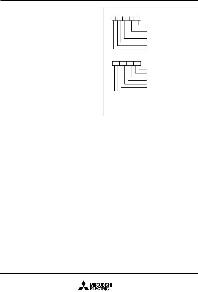
MITSUBISHI MICROCOMPUTERS
7560 Group
SINGLE-CHIP 8-BIT CMOS MICROCOMPUTER
I/O PORTS
Direction Registers
The I/O ports (ports P0, P1, P2, P4, P5, P6, P71–P77) have direction registers which determine the input/output direction of each individual pin. (Ports P00–P07 are shared with bit 0 of the port P0 direction register, and ports P10–P15 shared with bit 0 of the port
P1 direction register.) Each bit in a direction register corresponds to one pin, and each pin can be set to be input port or output port.
When “0” is written to the bit corresponding to a pin, that pin becomes an input pin. When “1” is written to that bit, that pin becomes an output pin.
If data is read from a pin set to output, the value of the port output latch is read, not the value of the pin itself. Pins set to input are floating. If a pin set to input is written to, only the port output latch is written to and the pin remains floating.
Port P3 Output Control Register
Bit 0 of the port P3 output control register (address 000716) enables control of the output of ports P30–P37.
When the bit is set to “1”, the port output function is valid.
When resetting, bit 0 of the port P3 output control register is set to “0” (the port output function is invalid) and pulled up.
Pull-up Control
b7 |
b0 |
PULL register A
(PULLA : address 001616)
P00, P01 pull-up
P02, P03 pull-up
P04–P07 pull-up
P10–P13 pull-up
P14, P15 pull-up
P16, P17 pull-up
P20–P23 pull-up
P24–P27 pull-up
b7 |
b0 |
PULL register B
(PULLB : address 001716)
P41–P43 pull-up
P44–P47 pull-up
P50–P53 pull-up
P54–P57 pull-up
P60–P63 pull-up
P64–P67 pull-up
Not used (return “0” when read)
0 : Disable
1 : Enable
Note: The contents of PULL register A and PULL register B do not affect ports programmed as the output port.
Fig. 11 Structure of PULL register A and PULL register B
By setting the PULL register A (address 001616) or the PULL register B (address 001716), ports P0 to P2, P4 to P6 can control pullup with a program.
However, the contents of PULL register A and PULL register B do not affect ports programmed as the output ports.
The PULL register A setting is invalid for pins set to segment output with the segment output enable register.
14

MITSUBISHI MICROCOMPUTERS
7560 Group
SINGLE-CHIP 8-BIT CMOS MICROCOMPUTER
Table 6 List of I/O port function (1)
Pin |
Name |
Input/Output |
I/O Format |
Non-Port Function |
Related SFRs |
Diagram No. |
|||
P00/SEG26– |
Port P0 |
Input/output, |
CMOS compatible |
LCD segment output |
PULL register A |
(1) |
|||
P07/SEG33 |
|
byte unit |
input level |
|
Segment output enable |
(2) |
|||
|
|
|
|
|
|
|
|||
|
|
|
|
CMOS 3-state output |
|
register |
|
||
|
|
|
|
|
|
|
|
|
|
P10/SEG34– |
Port P1 |
Input/output, |
CMOS compatible |
LCD segment output |
PULL register A |
(1) |
|||
P15/SEG39 |
|
6-bit unit |
input level |
|
Segment output enable |
(2) |
|||
|
|
|
|
|
|
|
|||
|
|
|
|
CMOS 3-state output |
|
register |
|
||
|
|
|
|
|
|
|
|||
P16 , P17 |
|
Input/output, |
CMOS compatible |
|
PULL register A |
(4) |
|||
|
|
individual bits |
input level |
|
|
|
|
||
|
|
|
|
CMOS 3-state output |
|
|
|
|
|
|
|
|
|
|
|
|
|
|
|
P20–P27 |
Port P2 |
Input/output, |
CMOS compatible |
Key input (key-on |
PULL register A |
|
|||
|
|
individual bits |
input level |
wake-up) interrupt |
Interrupt control register2 |
|
|||
|
|
|
|
CMOS 3-state output |
input |
|
|||
|
|
|
|
Key input control register |
|
||||
|
|
|
|
|
|
||||
|
|
|
|
|
|
|
|
||
|
|
|
|
|
|
|
|
|
|
P30/SEG18– |
Port P3 |
Output |
CMOS 3-state output |
LCD segment output |
Segment output enable |
(3) |
|||
P37/SEG25 |
|
|
|
|
|
|
register |
|
|
|
|
|
|
|
|
|
P3 output enable register |
|
|
|
|
|
|
|
|
|
|
||
P40 |
Port P4 |
Input/output, |
CMOS compatible |
|
|
|
(13) |
||
|
|
individual bits |
input level |
|
|
|
|
||
|
|
|
|
N-channel open-drain |
|
|
|
|
|
|
|
|
|
output |
|
|
|
|
|
|
|
|
|
|
|
|
|
|
|
P41/INT1, |
|
|
|
CMOS compatible |
External interrupt input |
Interrupt edge selection |
(4) |
||
P42/INT2 |
|
|
|
input level |
|
register |
|
||
|
|
|
|
|
|
|
|
|
|
P43/φ /TOUT |
|
|
|
CMOS 3-state output |
Timer output |
PULL register B |
(12) |
||
|
|
|
|
|
|
φ output |
Timer 123 mode register |
|
|
|
|
|
|
|
|
|
TOUT/φ output control |
|
|
|
|
|
|
|
|
|
register |
|
|
P44/RXD, |
|
|
|
|
|
Serial I/O1 function I/O |
PULL register B |
(5) |
|
P45/TXD, |
|
|
|
|
|
|
|
|
|
|
|
|
|
|
|
Serial I/O1 control register |
(6) |
||
P46/SCLK1, |
|
|
|
|
|
|
|||
|
|
|
|
|
|
Serial I/O1 status register |
|
(7) |
|
P47/SRDY1 |
|
|
|
|
|
|
|||
|
|
|
|
|
|
UART control register |
(8) |
||
|
|
|
|
|
|
|
|||
|
|
|
|
|
|
|
|
||
P50/PWM0, |
Port P5 |
Input/output, |
CMOS compatible |
PWM output |
PULL register B |
(10) |
|||
P51/PWM1 |
|
individual bits |
input level |
|
PWM control register |
|
|||
|
|
|
|
CMOS 3-state output |
|
|
|||
|
|
|
|
|
|
|
|
||
P52/RTP0, |
|
|
|
Real time port |
PULL register B |
(9) |
|||
|
|
|
|
|
|||||
P53/RTP1 |
|
|
|
|
|
function output |
Timer X mode register |
|
|
|
|
|
|
|
|
|
|
||
|
|
|
|
|
|
|
|
|
|
P54/CNTR0 |
|
|
|
|
|
Timer X function I/O |
PULL register B |
(11) |
|
|
|
|
|
|
|
|
Timer X mode register |
|
|
|
|
|
|
|
|
|
|
|
|
P55/CNTR1 |
|
|
|
|
|
Timer Y function input |
PULL register B |
(14) |
|
|
|
|
|
|
|
|
|
|
|
|
|
|
|
|
|
|
Timer Y mode register |
|
|
|
|
|
|
|
|
|
|
|
|
P56/DA1 |
|
|
|
|
|
DA1 output |
PULL register B |
(15) |
|
|
|
|
|
|
|
|
D-A control register |
|
|
P57/ADT/ |
|
|
|
|
|
DA2 output |
PULL register B |
(15) |
|
DA2 |
|
|
|
|
|
A-D trigger input |
D-A control register |
|
|
|
|
|
|
|
|
|
|||
|
|
|
|
|
|
|
A-D control register |
|
|
|
|
|
|
|
|
|
|
|
|
15

MITSUBISHI MICROCOMPUTERS
7560 Group
SINGLE-CHIP 8-BIT CMOS MICROCOMPUTER
Table 7 List of I/O port function (2)
Pin |
Name |
Input/Output |
I/O Format |
Non-Port Function |
Related SFRS |
Diagram No. |
|
|
|
|
|
|
|
P60/SIN2/AN0 |
Port P6 |
Input/ |
CMOS compatible input |
A-D conversion input |
PULL register B |
(17) |
|
|
output, |
level |
Serial I/O2 function I/O |
A-D control register |
|
|
|
individual |
CMOS 3-state output |
|
Serial I/O2 control |
|
P61/SOUT2/ |
|
|
(18) |
|||
|
bits |
|
|
register |
||
AN1 |
|
|
|
|
|
|
|
|
|
|
|
|
|
P62/SCLK21/ |
|
|
|
|
|
(19) |
AN2 |
|
|
|
|
|
|
|
|
|
|
|
|
|
P63/SCLK22 / |
|
|
|
|
|
(20) |
AN3 |
|
|
|
|
|
|
|
|
|
|
|
|
|
P64/AN4– |
|
|
|
A-D conversion input |
A-D control register |
(16) |
P67/AN7 |
|
|
|
|
PULL register B |
|
|
|
|
|
|
|
|
|
|
|
|
|
|
|
P70/INT0 |
Port P7 |
Input |
CMOS compatible input |
External interrupt input |
Interrupt edge |
(23) |
|
|
|
level |
|
selection register |
|
|
|
|
|
|
|
|
P71–P77 |
|
Input/ |
CMOS compatible input |
|
|
(13) |
|
|
output, |
level |
|
|
|
|
|
individual |
N-channel open-drain |
|
|
|
|
|
bits |
|
|
|
|
|
|
output |
|
|
|
|
|
|
|
|
|
|
|
|
|
|
|
|
|
|
COM0–COM3 |
Common |
Output |
LCD common output |
|
LCD mode register |
(21) |
|
|
|
|
|
|
|
SEG0–SEG17 |
Segment |
Output |
LCD segment output |
|
|
(22) |
|
|
|
|
|
|
|
Notes1: How to use double-function ports as function I/O ports, refer to the applicable sections.
2:Make sure that the input level at each pin is either 0 V or VCC during execution of the STP instruction. When an input level is at an intermediate potential, a current will flow VCC to VSS through the input-stage gate.
16
MITSUBISHI MICROCOMPUTERS
7560 Group
SINGLE-CHIP 8-BIT CMOS MICROCOMPUTER
(1) Ports P01–P07, P11–P15 |
|
|
|
|
|
|
|
Pull-up |
|
|
|
|
|
|
|
|
|||||||||||||||
|
|
|
|
|
|
|
|
|
|
|
|
|
|
|
|
|
|
|
|
|
|
|
|
|
|
|
|||||
|
|
|
|
|
|
|
|
|
|
|
|
|
LCD drive timing |
|
VL2/VL3/VCC |
|
|
|
|
|
|
|
|
|
|||||||
|
Segment data |
|
|
|
|
|
|
Segment/Port |
|
|
|
|
|
|
|
|
|
||||||||||||||
|
|
|
|
|
|
|
|
|
|
|
|
|
|
|
|
|
|
|
|
||||||||||||
|
|
|
|
|
|
|
|
|
|
|
|
|
|
|
|
|
|
|
|
|
|
|
|||||||||
|
|
|
|
|
|
|
|
|
|
|
|
|
|
|
|
|
|
|
|
|
|
|
|
|
|||||||
|
|
|
|
|
|
|
|
|
|
|
|
|
|
|
|
|
|
|
|
|
|
|
|
|
|||||||
|
|
|
|
|
|
|
|
|
|
|
|
|
Interface logic level |
|
|
Segment |
|
|
|
|
|
|
|
|
|||||||
|
|
|
|
|
|
|
|
|
|
|
|
|
|
|
|
|
|
|
|
|
|
||||||||||
|
Data bus |
|
|
Port latch |
|
|
|
|
|
shift circuit |
|
|
|
|
|
|
|
|
|
|
|
|
|
|
|
||||||
|
|
|
|
|
|
|
|
|
|
|
|
|
|
|
|
|
|
|
|
|
|
||||||||||
|
Port |
direction register |
|
|
|
|
|
|
|
|
|
VL1/VSS |
|
|
|
|
|
|
|
|
|
|
|||||||||
|
|
|
|
|
|
|
|
|
|
|
|
|
|
|
|
|
|
|
|||||||||||||
|
|
|
|
|
|
|
|
|
|
|
|
|
|
|
|
|
|
Port |
|
|
|
|
|
|
|
|
|||||
|
|
|
|
|
|
|
|
|
|
|
|
Port/Segment |
|
|
|
|
|
|
|
|
|
|
|
||||||||
|
|
|
|
|
|
|
|
|
|
|
|
|
|
|
|
|
|
|
|
|
|
||||||||||
|
|
|
|
|
|
|
|
|
|
|
|
|
|
|
Port direction register |
|
|
|
|
|
|
|
|
||||||||
|
|
|
|
|
|
|
|
|
|
|
|
|
|
|
|
|
|
|
|
|
|
|
|
|
|
|
|
|
|
|
|
(2) Ports P00, P10
Pull-up
|
|
|
|
|
|
|
|
|
|
|
|
|
LCD drive timing |
|
VL2/VL3/VCC |
|
|
|
|
|
|
|
|
|
|
|
|
|
|
||||||
|
|
|
|
|
Direction register |
|
|
|
|
|
|
|
|
|
|
Segment/Port |
|
|
|
|
|
|
|
|
|
|
|
|
|||||||
|
|
|
|
|
|
|
|
|
|
|
|
|
|
|
|
|
|
|
|
|
|
|
|
|
|
|
|
|
|
|
|
|
|
|
|
|
|
|
|
Segment data |
|
|
|
|
|
|
|
Interface logic level |
|
|
|
|
|
|
|
|
|
|
|
|
|
|
|
|
|
|
|
||||
|
|
|
|
|
|
|
|
|
|
|
|
|
|
|
|
|
|
|
|
|
|
|
|
|
|
|
|
|
|
||||||
Data bus |
|
|
|
|
Port latch |
|
|
|
|
|
|
|
|
shift circuit |
|
Segment |
|
|
|
|
|
|
|
|
|
|
|
|
|
||||||
|
|
|
|
|
|
|
|
|
|
|
|
|
|
|
|
|
|
|
|
VL1/VSS |
|
|
|
|
|
|
|
|
|
|
|
|
|
||
|
|
|
|
|
|
|
|
|
|
|
|
|
Port/Segment |
|
|
|
Port |
|
|
|
|
|
|
|
|
|
|
|
|
||||||
|
|
|
|
|
|
|
|
|
|
|
|
|
|
|
|
|
|
|
|
|
|
|
|
||||||||||||
|
|
|
|
|
|
|
|
|
|
|
|
|
|
Port direction register |
|
|
|
|
|
|
|
|
|
|
|
|
|
|
|
|
|
|
|||
|
|
|
|
|
|
|
|
|
|
|
|
|
|
|
|
|
|
|
|
|
|
|
|
|
|
|
|
|
|
|
|
||||
|
|
|
|
|
|
|
|
|
|
|
|
|
|
|
|
|
|
|
|
|
|
|
|
|
|
|
|
|
|
|
|
|
|
|
|
(3) Port P3 |
|
|
|
|
|
|
|
|
|
|
|
|
|
|
|
|
|
Pull-up |
|
|
|
|
|
|
|
|
|
|
|
|||||||
|
|
|
|
|
|
|
|
|
|
|
|
|
|
|
|
|
|
|
|
|
|
|
|
|
|
|
|
|
|
|
|
|
||||
|
|
|
|
|
|
|
|
|
|
|
|
|
LCD drive timing |
|
|
VL2/VL3/VCC |
|
|
|
|
|
|
|
|
|
|
|
|
|
|||||||
|
Segment data |
|
|
|
|
|
|
|
|
|
|
|
|
Segment/Port |
|
|
|
|
|
|
|
|
|
|
|
|||||||||||
|
|
|
|
|
|
|
|
|
|
|
|
|
|
|
|
|
|
|
|
|
|
|
|
|
|
|
|
|
|
|||||||
|
|
|
|
|
|
|
|
|
|
|
|
|
|
|
|
|
|
|
|
|
|
|
|
|
|
|
|
|
|
|||||||
|
|
|
|
|
|
|
|
|
|
|
|
|
|
|
|
|
|
|
|
|
|
|
|
|
|
|
|
|
|
|||||||
|
|
|
|
|
|
|
|
|
|
|
|
|
Interface logic level |
|
|
|
|
|
|
|
|
|
|
|
|
|
|
|
|
|
|
|||||
|
|
|
|
|
|
|
|
|
|
|
|
Segment |
|
|
|
|
|
|
|
|
|
|
|
|||||||||||||
|
Data bus |
|
|
|
Port latch |
|
|
|
|
|
|
shift circuit |
|
|
|
|
|
|
|
|
|
|
|
|
|
|
|
|
|
|
||||||
|
|
|
|
|
|
|
|
|
|
|
|
|
|
|
|
|
|
|
|
|
|
|
|
|
|
|
|
|||||||||
|
|
|
|
|
|
|
|
|
|
|
|
|
|
|
|
|
|
|
|
|
|
VL1/VSS |
|
|
|
|
|
|
|
|
|
|
|
|
||
|
|
|
|
|
|
|
|
|
|
|
Port/Segment |
|
|
|
Port |
|
|
|
|
|
|
|
|
|
|
|
||||||||||
|
|
|
|
|
|
|
|
|
|
|
|
|
|
|
|
|
|
|
|
|
|
|
|
|||||||||||||
|
|
|
|
|
|
|
|
|
|
|
|
|
|
|
|
|
Output control |
|
|
|
|
|
|
|
|
|
|
|
|
|
|
|
||||
(4) Ports P16,P17,P2,P41,P42 |
|
|
|
|
|
|
|
|
|
|
|
|
|
|
|
|
|
|
|
|
|
|
|
|||||||||||||
|
|
|
|
|
|
|
|
|
|
(5) Port P44 |
|
|
|
|
|
|
|
|
|
|
|
|||||||||||||||
|
|
|
|
|
|
|
|
|
|
|
|
|
|
|
|
|
|
|
|
|
||||||||||||||||
|
|
|
|
|
|
|
|
|
|
|
|
|
|
|
|
|
|
|
|
|
|
|
|
|
|
|
|
|
|
|
|
|
|
|
|
|
Direction register
Data bus |
Port latch |
Pull-up control |
Pull-up control |
Serial I/O1 enable bit |
|
Reception enable bit |
|
|
Direction |
|
register |
Data bus |
Port latch |
Key-on wake up interrupt input |
Serial I/O1 input |
|
INT1, INT2 interrupt input |
||
|
||
Except P16, P17 |
|
Fig. 12 Port block diagram (1)
17
MITSUBISHI MICROCOMPUTERS
7560 Group
SINGLE-CHIP 8-BIT CMOS MICROCOMPUTER
(6) Port P45 |
|
(7) Port P46 |
|
|
|
|
||||||
|
|
|
|
|
|
|
|
Serial I/O1 synchronization |
|
|
||
|
|
|
Pull-up control |
|
|
|
clock selection bit |
|
|
|
Pull-up control |
|
P45/TxD P-channel output disable bit |
|
|
|
|
|
Serial I/O1 enable bit |
|
|
|
|||
|
|
|||||||||||
|
|
|
|
|
|
|
|
|
|
|
|
|
|
|
|
|
|
|
|
|
|
|
|
|
|
Serial I/O1 enable bit |
Serial I/O1 mode selection bit |
|
Transmission enable bit |
||
Serial I/O1 enable bit |
||
Direction |
||
Direction |
||
register |
register |
Data bus |
Port latch |
Data bus |
Port latch |
|
|
|
|
|
|
|
|
|
|
|
|
|
|
|
|
|
|
|
|
|
|
|
|
|
|
|
|
|
|
|
|
|
|
|
|
|
|
|
|
|
|
|
|
|
|
|
|
|
|
|
|
|
|
|
|
|
|
|
|
|
|
|
|
|
|
|
|
|
|
|
|
|
|
|
|
|
|
|
|
|
|
|
|
|
|
|
|
|
|
|
|
|
|
|
|
|
|
|
|
|
|
|
|
|
|
|
|
|
|
|
|
|
|
|
|
|
|
|
|
|
|
|
|
|
|
|
|
|
|
|
|
|
|
|
|
|
|
|
|
|
|
|
|
|
|
|
|
|
|
Serial I/O1 output |
|
|
|
|
|
|
|
|
|
|
|
|
|
|
|
|
|
|
|
|
|
|
|
|
|
|
|
|
|
|
|
|
|
|
|
|
|
|
|
|
|
|
|
|
|
|
|||
|
|
|
|
|
|
|
|
|
|
Serial I/O1 clock output |
|
|
|
|
|
|
|
|
|
|
|
|||
|
|
|
|
|
|
|
|
|
|
|
|
|
|
|
|
|
|
|
|
|||||
|
|
|
|
|
|
|
|
|
|
|
|
|
|
|
|
|
|
|
|
|
|
|
||
|
|
|
|
|
|
|
|
|
|
|
|
|
|
|
|
|
|
|
|
|
||||
|
|
|
|
|
|
|
|
|
|
|
|
|
|
|
|
|
|
|
|
|
|
|
|
|
|
|
|
|
|
|
|
|
|
|
|
|
|
|
|
|
|
|
|
|
|
|
|
|
|
|
|
|
|
|
|
|
|
|
|
|
|
|
|
|
|
|
|
|
|
|
|
|
|
|
|
|
|
|
|
|
|
|
|
|
|
|
|
|
|
|
|
|
|
|
|
|
|||
|
|
|
|
|
|
|
|
|
|
|
|
|
|
|
|
|
|
Serial I/O1 clock input |
|
|||||
|
|
|
|
|
|
|
|
|
|
|
|
|
|
|
|
|
|
|
|
|
||||
|
|
|
|
|
|
|
|
|
|
|
|
|
|
|
|
|
|
|
|
|
|
|
|
|
(8) Port P47 |
|
(9) Ports P52,P53 |
Pull-up control |
|
|
|
Pull-up control |
|
|
Serial I/O1 mode selection bit |
|
|
||
|
|
|
||
Serial I/O1 enable bit |
|
|
|
|
SRDY1 output enable bit |
|
Direction |
|
|
|
Direction |
|
register |
|
|
register |
|
|
|
Data bus |
Port latch |
Data bus |
Port latch |
|
|
|
|
||
|
|
Real time control bit |
|
|
Serial I/O1 ready output |
Real time port data |
|
||
|
|
|
||
(10) Ports P50,P51 |
(11) Port P54 |
Pull-up control |
||
Pull-up control |
|
|
||
|
|
|
|
|
|
|
|
Direction |
|
|
|
|
register |
|
|
Direction |
|
|
|
|
register |
|
|
|
|
|
Data bus |
Port latch |
|
Data bus |
Port latch |
|
|
|
|
|
|
Pulse output mode |
|
|
|
|
Timer output |
|
PWM function enable bit |
|
|
CNTR0 interrupt input |
|
|
PWM output |
|
|
|
|
|
|
|
|
Fig. 13 Port block diagram (2)
18
MITSUBISHI MICROCOMPUTERS
7560 Group
SINGLE-CHIP 8-BIT CMOS MICROCOMPUTER
(12) Port P43 |
Pull-up control |
(13) Ports P40,P71–P77 |
|
|
|
|
|
|
Direction |
|
Direction |
|
|
register |
|
|
register |
|
|
|
|
|
|
Data bus |
Port latch |
Data bus |
Port latch |
|
|
||
TOUT/φ output control |
|
|
|
Timer output |
|
|
|
TOUT/φ selection bit |
|
|
|
φ |
output |
|
|
(14) Port P55 |
|
(15) Ports P56,P57 |
|
Pull-up control |
|
Pull-up control |
|
|
|
|
|
|
Direction |
|
Direction |
|
|
register |
|
|
register |
|
|
|
|
|
|
Data bus |
Port latch |
Data bus |
Port latch |
|
|
||
|
CNTR1 interrupt input |
|
A-D trigger input |
|
|
Except P56 |
|
|
|
|
|
|
|
|
D-A converter output |
|
|
|
D-A1,D-A2 output enable bit |
(16) Ports P64–P67 |
(17) Port P60 |
|
|
|
Pull-up control |
|
Pull-up control |
|
Direction |
|
Direction |
|
register |
|
|
|
|
register |
|
|
|
|
|
Data bus |
Port latch |
Data bus |
Port latch |
|
A-D conversion input |
|
Serial I/O2 input |
|
Analog input pin selection bit |
|
|
|
|
|
|
|
|
|
A-D conversion input |
|
|
|
Analog input pin selection bit |
Fig. 14 Port block diagram (3)
19
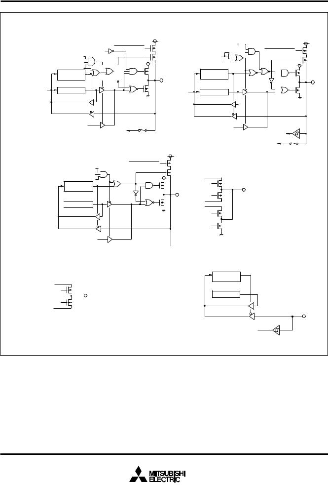
MITSUBISHI MICROCOMPUTERS
7560 Group
SINGLE-CHIP 8-BIT CMOS MICROCOMPUTER
(18) Port P61
P61/SOUT2 P-channel output disable bit |
Pull-up control |
|
|
||
Serial I/O2 transmit end signal |
|
|
Synchronous clock selection bit |
|
|
Serial I/O2 port selection bit |
|
|
|
Direction |
|
|
register |
|
Data bus |
Port latch |
|
(19) Port P62
Synchronous clock selection bit
|
Pull-up control |
Serial I/O2 port selection bit |
|
Synchronous clock output pin |
|
|
selection bit |
|
Direction |
|
register |
Data bus |
Port latch |
Serial I/O2 output |
Serial I/O2 clock output |
|
A-D conversion input |
Serial I/O2 clock input |
|
Analog input pin selection bit |
||
|
||
|
A-D conversion input |
|
|
Analog input pin selection bit |
(20) Port P63
Pull-up control
Synchronous clock selection bit Serial I/O2 port selection bit 
Synchronous clock output pin selection bit Direction register
Data bus  Port latch
Serial I/O2 clock output
A-D conversion input 


Analog input pin selection bit
(21)COM0–COM3
VL3
The gate input signal of each transistor is controlled by the LCD
duty ratio and the bias value.
VL2
VL1
VSS
(22)SEG0–SEG17
VL2/VL3
The voltage applied to the sources of P-

 channel and N-channel transistors is the controlled voltage by the bias value.
VL1/VSS
(23) Port P70
Direction
register
Data bus  Port latch
INT0 input
Fig. 15 Port block diagram (4)
20
Loading...