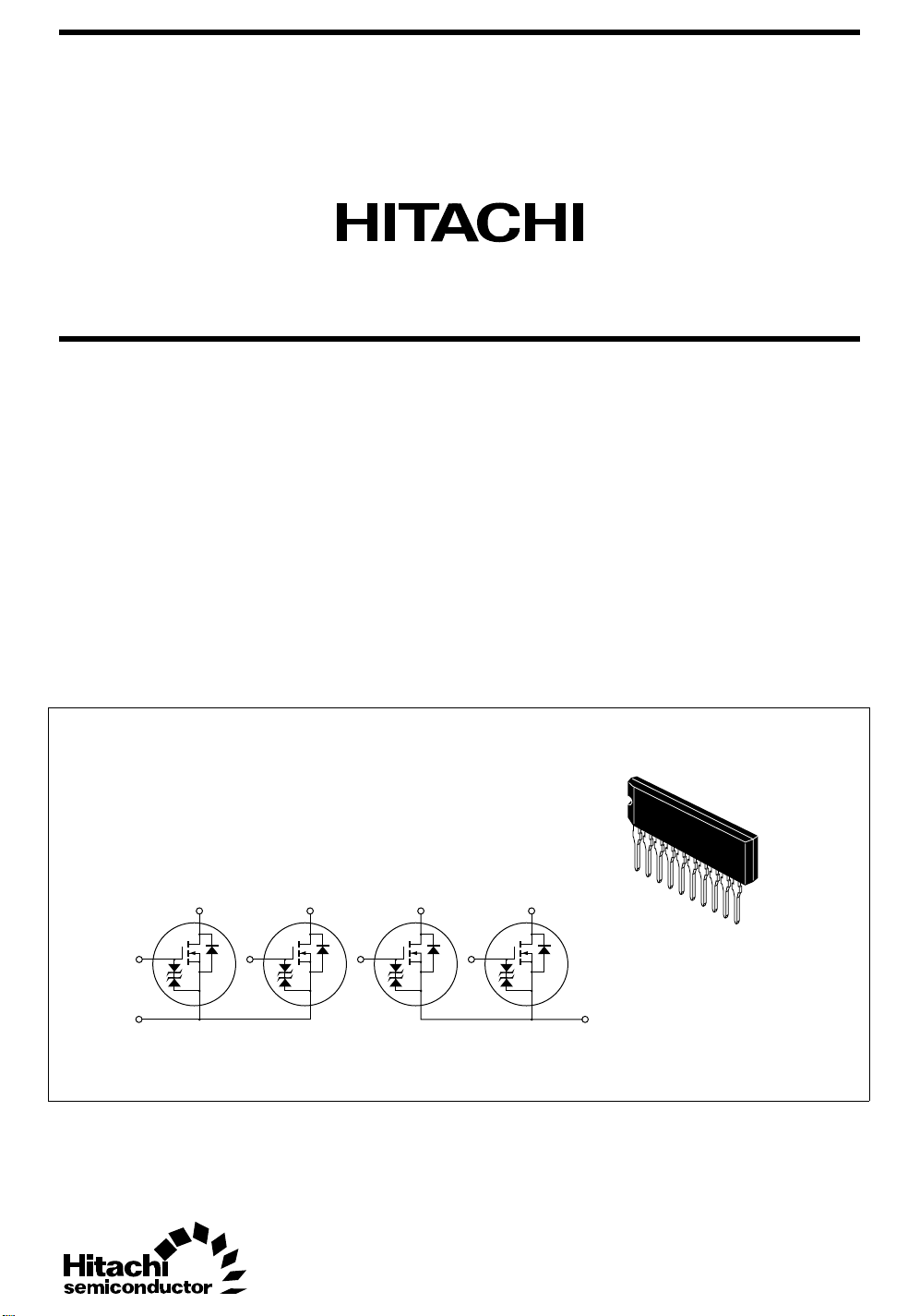
HIT 4AK25 Datasheet

Silicon N-Channel Power MOS FET Array
Application
High speed power switching
Features
• Low on-resistance
R
0.45 , VGS = 10 V, ID = 1 A
DS(on)
• Low drive current
• High speed switching
• High density mounting
4AK25
Outline
SP-10
2 G
1 S
1
2
3
D
4
G
5
D
6
G
7
D
8
G
9
D
S 10
3
4
5
6
7
8
9
1, 10. Source
2, 4, 6, 8. Gate
3, 5, 7, 9. Drain
10

4AK25
Absolute Maximum Ratings (Ta = 25°C)
Item Symbol Ratings Unit
Drain to source voltage V
Gate to source voltage V
Drain current I
Drain peak current I
Body to drain diode reverse drain current I
DSS
GSS
D
D(pulse)
DR
1
*
Channel dissipation Pch (Tc = 25°C)*224 W
Channel dissipation Pch*
2
Channel temperature Tch 150 °C
Storage temperature Tstg –55 to +150 °C
Notes: 1. PW ≤ 10 µs, duty cycle ≤ 1%
2. 4 Devices operation
60 V
±20 V
1.5 A
4.5 A
1.5 A
3.6 W
2
 Loading...