

3SK309
GaAs N Channel Dual Gate MES FET
UHF RF Amplifier
Features
• Capable of low voltage operation (VDS = 1.5 to 3 V)
• Excellent low noise characteristics (NF = 1.25 dB typ. at f = 900 MHz)
• High power gain (PG = 21.0 dB typ. at f = 900 MHz)
Outline
CMPAK–4
ADE-208-472 A
2nd. Edition
2
3
1
4
1. Source
2. Gate1
3. Gate2
4. Drain

3SK309
Absolute Maximum Ratings (Ta = 25°C)
Item Symbol Ratings Unit
Drain to source voltage V
Gate 1 to source voltage V
Gate 2 to source voltage V
Drain current I
DS
G1S
G2S
D
Channel power dissipation Pch 100 mW
Channel temperature Tch 125 °C
Storage temperature Tstg –55 to +125 °C
Electrical Characteristics (Ta = 25°C)
Item Symbol Min Typ Max Unit Test conditions
Gate 1 to cutoff current I
Gate 2 to cutoff current I
Gate 1 to source cutoff voltage V
Gate 2 to source cutoff voltage V
Zero gate voltege drain current I
G1SS
G2SS
G1S(off)
G2S(off)
DSS
Forward transfer admittance |yfs| 30 40 — mS VDS = 3 V, V
Power gain PG 18 21 — dB VDS = 3 V, V
Noise figure NF — 1.25 1.5 dB ID = 5 mA, f = 900 MHz
Power gain PG — 20 — dB VDS = 1.5 V, V
Noise figure NF — 1.3 — dB ID = 3 mA, f = 900 MHz
Note: Marking is “XV–”
— — –20 µAV
— — –20 µAV
–0.2 — –1.5 V VDS = 3 V, V
–0.2 — –1.5 V VDS = 3 V, V
25 40 60 mA VDS = 3 V, V
6V
–4 V
–4 V
18 mA
= –4 V
G1S
V
= VDS = 0
G2S
= –4 V
G2S
V
= VDS = 0
G1S
= 0
I
= 100 µA
D
I
= 100 µA
D
V
= 0
G2S
I
= 5 mA, f = 1 kHz
D
G2S
G1S
G1S
G2S
G2S
= 0
= 0
= 0
= 0
G2S
= 0
2
Main Characteristics
3SK309
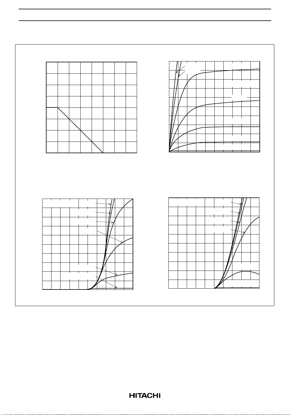
Maximum Channel Power
Dissipation Curve
200
150
100
50
Channel Power Dissipation Pch (mW)
0 50 100 150 200
Ambient Temperature Ta (°C)
Drain Current vs.
Gate1 to Source Voltage
20
16
(mA)
D
12
VDS = 3 V
0 V
–0.2 V
–0.4 V
–0.6 V
Typical Output Characteristics
20
–0.4 V
–0.6 V
–0.5 V
16
Pulse Test
(mA)
D
12
–0.7 V
8
–0.8 V
Drain Current I
4
V
G1S
–0.9 V
= –1 V
012345
Drain to Source Voltage V
DS
(V)
Drain Current vs.
Gate2 to Source Voltage
20
VDS = 3 V
16
0 V
–0.2 V
–0.4 V
(mA)
D
12
–0.6 V
8
Drain Current I
4
V
G2S
0
–2.0
–1.6 –1.2 –0.8 –0.4 0
Gate1 to Source Voltage V
–0.8 V
= –1 V
G1S
(V)
8
Drain Current I
4
0
–2.0
–1.6 –1.2 –0.8 –0.4 0
Gate2 to Source Voltage V
V
G1S
–0.8 V
= –1 V
(V)
G2S
3
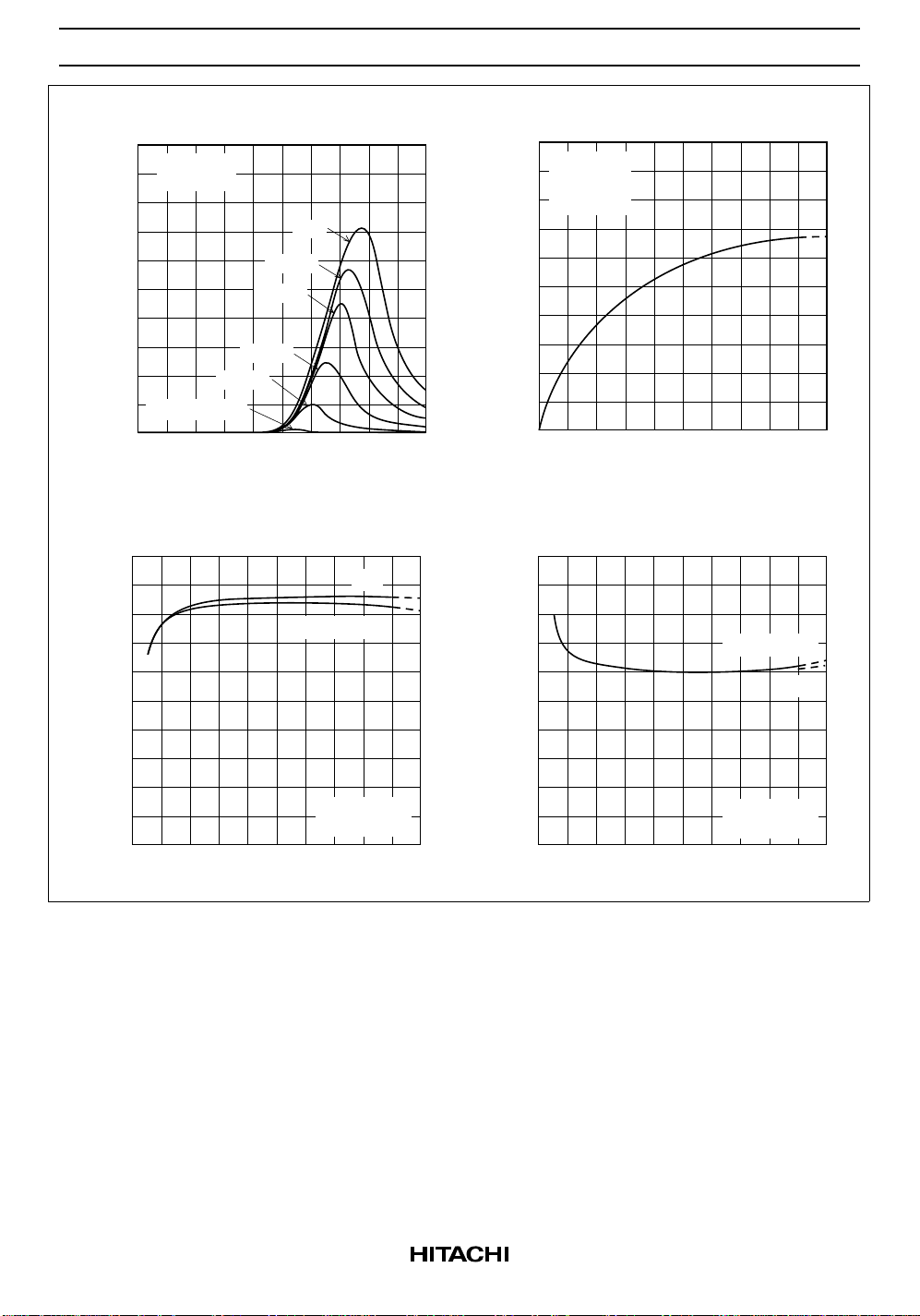
3SK309
Forward Transfer Admittance vs.
Gate1 to Source Voltage
100
VDS = 3 V
fs
f = 1 kHz
80
0 V
60
–0.2 V
–0.4 V
40
–0.6 V
20
V
Forward Transfer Admittance |y | (mS)
G2S
0
–2.0
Gate1 to Source Voltage V
25
–0.8 V
= –1 V
–1.6 –1.2 –0.8 –0.4 0
G1S
Power Gain vs. Drain Current
3 V
20
V = 1.5 V
DS
15
(V)
Forward Transfer Admittance vs.
Drain Current
100
VDS = 3 V
V
fs
80
= 0
G2S
f = 1 kHz
60
40
20
Forward Transfer Admittance |y | (mS)
0
4 8 12 16 20
Drain Current ID (mA)
2.0
Noise Figure vs. Drain Current
1.6
V = 1.5 V
DS
1.2
3 V
10
Power Gain PG (dB)
5
0
4 8 12 16 20
Drain Current I (mA)
V = 0
G2S
f = 900 MHz
D
0.8
Noise Figure NF (dB)
0.4
0
4 8 12 16 20
Drain Current I (mA)
V = 0
G2S
f = 900 MHz
D
4
 Loading...