HIT 3SK317 Datasheet

Silicon N-Channel Dual Gate MOS FET
UHF / VHF RF Amplifier
Features
• Low noise characteristics;
(NF = 1.0 dB typ. at f = 200 MHz)
• High power gain characteristics ;
(PG = 27.6 dB typ. at f = 200 MHz)
Outline
3SK317
ADE-208-778 (Z)
1st. Edition
Mar. 1999
Note: Marking is “ZR-”.
CMPAK-4
2
3
1
4
1. Source
2. Gate1
3. Gate2
4. Drain

3SK317
G
G
G1S
G2S
S
G2S
S
G1S
S
G1S
S
G2S
S
G2S
Absolute Maximum Ratings (Ta = 25°C)
Item Symbol Ratings Unit
Drain to source voltage V
Gate1 to source voltage V
Gate2 to source voltage V
Drain current I
DS
G1S
G2S
D
Channel power dissipation Pch 100 mW
Channel temperature Tch 150 °C
Storage temperature Tstg –55 to +150 °C
Electrical Characteristics (Ta = 25°C)
Item Symbol Min Typ Max Unit Test Conditions
Drain to source breakdown voltage V
Gate1 to source breakdown
(BR)DSS
V
(BR)G1SS
voltage
Gate2 to source breakdown
V
(BR)G2SS
voltage
Gate1 to source cutoff current I
Gate2 to source cutoff current I
Gate1 to source cutoff voltage V
Gate2 to source cutoff voltage V
Drain current I
G1SS
G2SS
G1S(off)
G2S(off)
DS(op)
Forward transfer admittance |yfs|2025—mSV
Input capacitance C
Output capacitance C
Reverse transfer capacitance C
iss
oss
rss
Power gain PG 24 27.6 — dB VDS = 6 V, V
Noise figure NF — 1.0 1.5 dB ID = 10 mA , f = 200 MHz
Power gain PG 12 15.6 — dB VDS = 6 V, V
Noise figure NF — 3 4 dB ID = 10 mA , f = 900 MHz
Noise figure NF — 2.7 3.5 dB V
14——V I
±8——V I
±8——V I
——±100 nA V
——±100 nA V
0 0.2 1 V V
0 0.3 1 V V
4814mAV
2.4 3.1 3.5 pF VDS = 6 V, V
0.8 1.1 1.4 pF ID = 10 mA , f = 1 MHz
— 0.021 0.04 pF
14 V
±8V
±8V
25 mA
= 200 µA
D
V
= V
G1S
= ±10 µA
1
V
G2S
= ±10 µA
2
V
G1S
= -3 V
G2S
= VDS = 0
= VDS = 0
= ±6 V
V
= VDS = 0
G2S
= ±6 V
V
= VDS = 0
G1S
= 10 V, V
D
I
= 100 µA
D
= 10 V, V
D
I
= 100 µA
D
= 6 V, V
D
V
= 3 V
G2S
= 6 V, V
D
I
= 10 mA , f = 1 kHz
D
= 6 V, V
D
I
= 10 mA , f = 60 MHz
D
= 3 V
= 3 V
= 0.75 V
= 3 V
= 3 V
G2S
= 3 V
G2S
= 3 V
G2S
= 3 V
2

200
150
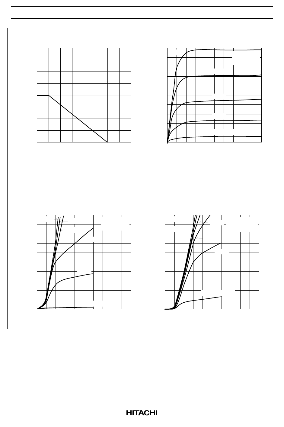
Maximum Channel Power
Dissipation Curve
3SK317
20
16
D
12
Typical Output Characteristics
1.2 V
1.0 V
V = 3 V
G2S
Pulse test
100
50
Channel power dissipation Pch (mW)
0
50 100 150 200
Ambient Temperature Ta (°C)
Drain Current vs. Gate1 to Source Voltage
20
16
3.0 V
2.5 V
2.0 V
V = 6 V
DS
Pulse test
1.5 V
D
12
8
1.0 V
8
0.8 V
Drain current I (mA)
4
0
210
0.6 V
V = 0.4 V
G1S
468
Drain to source voltage V (V)
Drain Current vs. Gate2 to Source Voltage
20
3.0 V
2.5 V
16
D
12
1.5 V
2.0 V
1.0 V
V = 6 V
DS
Pulse test
8
DS
Drain current I (mA)
4
V = 0.5 V
G2S
0
12345
Gate1 to source voltage V (V)
G1S
Drain current I (mA)
4
0
12345
V = 0.5 V
G1S
Gate2 to source voltage V (V)
G2S
3
 Loading...