


Diodes 74LVC1G32FS3-7, 74LVC1G32FW4-7, 74LVC1G32FW5-7, 74LVC1G32FX4-7, 74LVC1G32FZ4-7 Schematic [ru]
...
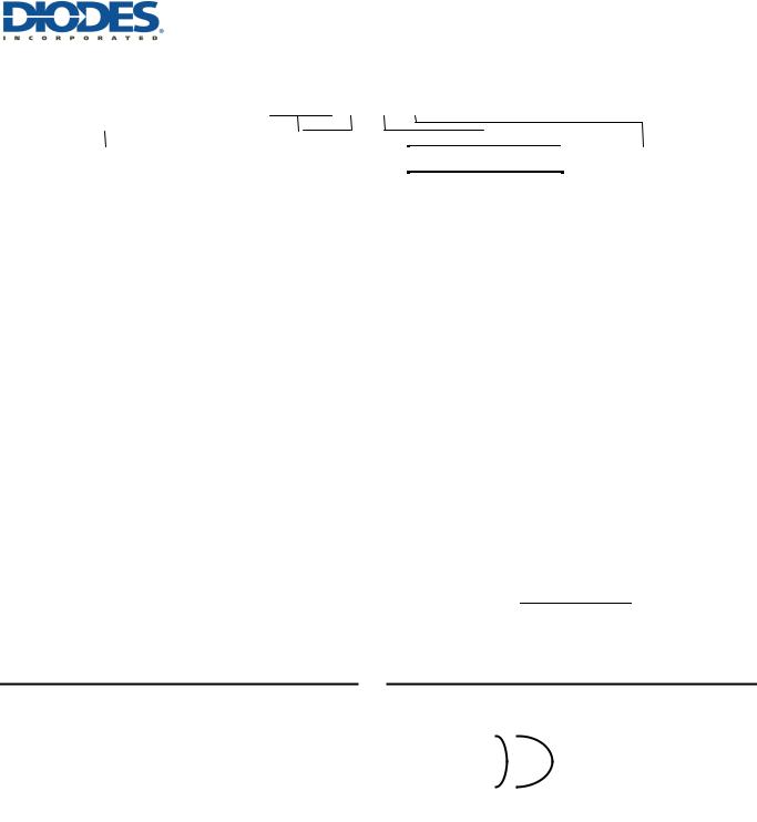
74LVC1G32
SINGLE 2 INPUT POSITIVE OR GATE
Description |
|
Pin Assignments |
The 74LVC1G32 is a single 2-input positive OR gate with a standard push-pull output. The device is designed for operation with a power supply range of 1.65V to 5.5V. The inputs are tolerant to 5.5V allowing this device to be used in a mixed voltage environment. The device is fully specified for partial power down applications using IOFF. The IOFF circuitry disables the output preventing damaging current backflow when the device is powered down.
The gate performs the positive Boolean function:
Y = A +B or Y = A •B
Features
• Wide Supply Voltage Range from 1.65 to 5.5V
• ± 24mA Output Drive at 3.3V
• CMOS Low Power Consumption
• IOFF Supports Partial-Power-Down Mode Operation
• Inputs Accept Up to 5.5V
•ESD Protection Tested per JESD 22
Exceeds 200-V Machine Model (A115)
Exceeds 2000-V Human Body Model (A114)
Exceeds 1000-V Charged Device Model (C101)
• Latch-Up Exceeds 100mA per JESD 78, Class I
• Range of Package Options
• Direct Interface with TTL Levels
• Totally Lead-Free & Fully RoHS Compliant (Notes 1 & 2)
• Halogen and Antimony Free. “Green” Device (Note 3)
Applications
• Voltage Level Shifting
• General Purpose Logic
• Power Down Signal Isolation
• Wide Array of Products Such as.
PCs, Networking, Notebooks, Netbooks, PDAsTablet Computers, E-readers
Computer Peripherals, Hard Drives, CD/DVD ROMTV, DVD, DVR, set top box
Cell Phones, Personal Navigation / GPSMP3 players ,Cameras, Video Recorders
Notes: |
1. |
No purposely added lead. Fully EU Directive 2002/95/EC (RoHS) & 2011/65/EU (RoHS 2) compliant. |
|
2. |
See http://www.diodes.com/quality/lead_free.html for more information about Diodes Incorporated’s definitions of Halogenand Antimony-free, "Green" |
|
|
and Lead-free. |
|
3. |
Halogenand Antimony-free "Green” products are defined as those which contain <900ppm bromine, <900ppm chlorine (<1500ppm total Br + Cl) and |
|
|
<1000ppm antimony compounds. |
74LVC1G32 |
1 of 14 |
July 2014 |
Document number: DS32200 Rev. 8 - 2 |
www.diodes.com |
© Diodes Incorporated |
|
|
|
|
|
|
|
|
|
|
|
|
|
|
|
|
|
|
|
|
74LVC1G32 |
||
|
|
|
|
|
|
|
|
|
|
|
|
|
|
|
|
|
|
|
|
|
|
|
|
Ordering Information |
|
|
|
|
|
|
|
|
|
|
|
|
|
|
|
|
|
||||
|
|
|
|
|
|
|
|
74 LVC1G 32 XXX -7 |
|
|
|
|
|
|
|
|||||||
|
|
|
|
|
|
|
|
|
|
|
|
|
|
|
|
|
|
|
|
|
|
|
|
|
|
|
|
|
|
|
|
|
|
|
|
|
|
|
|
|
|
|
|
|
|
|
|
|
Logic Device |
|
|
Function |
|
|
|
Package |
|
|
|
Packing |
|
|
||||||
|
|
|
74 : Logic Prefix |
|
|
32 : 2-Input |
|
|
W5 : SOT25 |
|
|
-7 : 7” Tape & Reel |
|
|
||||||||
|
|
|
LVC : 1.65 to 5.5 V |
|
|
OR Gate |
|
|
SE : SOT353 |
|
|
|
|
|
|
|
||||||
|
|
|
Logic Family |
|
|
|
|
|
|
|
|
Z : SOT553 |
|
|
|
|
|
|
|
|||
|
|
|
1G : One Gate |
|
|
|
|
|
|
|
FS3 : X2-DFN0808-4 |
|
|
|
|
|||||||
|
|
|
|
|
|
|
|
|
|
|
|
|
FW5 : X1-DFN1010-6 |
|
|
|
|
|||||
|
|
|
|
|
|
|
|
|
|
|
|
|
FW4 :X2-DFN1010-6 |
|
|
|
|
|||||
|
|
|
|
|
|
|
|
|
|
|
|
|
FX4 : X2- DFN1409-6 |
|
|
|
|
|||||
|
|
|
|
|
|
|
|
|
|
|
|
|
FZ4 : X2- DFN1410-6 |
|
|
|
|
|||||
|
|
|
|
|
|
|
|
|
|
|
|
|
|
|
|
|
|
|
|
|
||
|
|
Part Number |
Package |
|
|
Package |
|
Package |
|
|
7” Tape and Reel |
|
||||||||||
|
|
Code |
|
|
(Notes 4 & 5) |
|
|
Size |
Quantity |
|
Part Number Suffix |
|
||||||||||
|
|
|
|
|
|
|
|
|
|
|
||||||||||||
|
74LVC1G32W5-7 |
W5 |
|
|
SOT25 |
3.0mm X 2.8mm X 1.2mm |
3000/Tape & Reel |
-7 |
|
|
||||||||||||
|
|
|
0.95 mm lead pitch |
|
|
|||||||||||||||||
|
|
|
|
|
|
|
|
|
|
|
|
|
|
|
|
|
|
|||||
|
74LVC1G32SE-7 |
SE |
|
|
SOT353 |
2.0mm X 2.0mm X 1.1mm |
3000/Tape & Reel |
-7 |
|
|
||||||||||||
|
|
|
0.65 mm lead pitch |
|
|
|||||||||||||||||
|
|
|
|
|
|
|
|
|
|
|
|
|
|
|
|
|
|
|||||
|
74LVC1G32Z-7 |
Z |
|
|
SOT553 |
1.6mm X 1.6 mm X 0.62mm |
4000/Tape & Reel |
-7 |
|
|
||||||||||||
|
|
|
|
0.5 mm lead pitch |
|
|
||||||||||||||||
|
|
|
|
|
|
|
|
|
|
|
|
|
|
|
|
|
|
|
||||
|
74LVC1G32FS3-7 |
FS3 |
|
|
X2-DFN0808-4 |
0.9mm X 0.9 mm X 0.35mm |
5000/Tape & Reel |
-7 |
|
|
||||||||||||
|
|
|
0.5 mm pad pitch (diamond) |
|
|
|||||||||||||||||
|
|
|
|
|
|
|
|
|
|
|
|
|
|
|
|
|
|
|||||
|
74LVC1G32FW5-7 |
FW5 |
|
|
X1-DFN1010-6 |
1.0mm X 1.0mm X 0.5mm |
5000/Tape & Reel |
-7 |
|
|
||||||||||||
|
|
|
0.35 mm pad pitch |
|
|
|||||||||||||||||
|
|
|
|
|
|
|
|
|
|
|
|
|
|
|
|
|
|
|||||
|
74LVC1G32FW4-7 |
FW4 |
|
|
X2-DFN1010-6 |
1.0mm X 1.0mm X 0.4mm |
5000/Tape & Reel |
-7 |
|
|
||||||||||||
|
|
|
0.35 mm pad pitch |
|
|
|||||||||||||||||
|
|
|
|
|
|
|
|
|
|
|
|
|
|
|
|
|
|
|||||
|
74LVC1G32FX4-7 |
FX4 |
|
|
X2-DFN1409-6 |
1.4mm X 0.9mm X 0.4mm |
5000/Tape & Reel |
-7 |
|
|
||||||||||||
|
|
(Chip scale alternative) |
|
0.5 mm pad pitch |
|
|
||||||||||||||||
|
|
|
|
|
|
|
|
|
|
|
|
|
|
|
||||||||
|
74LVC1G32FZ4-7 |
FZ4 |
|
|
X2-DFN1410-6 |
1.4mm X 1.0mm X 0.4mm |
5000/Tape & Reel |
-7 |
|
|
||||||||||||
|
|
|
|
0.5 mm pad pitch |
|
|
||||||||||||||||
|
|
|
|
|
|
|
|
|
|
|
|
|
|
|
|
|
|
|
||||
Notes: |
|
4. Pad layout as shown on Diodes Inc. suggested pad layout document AP02001, which can be found on our website at |
|
|
|
|
||||||||||||||||
|
|
|
http://www.diodes.com/datasheets/ap02001.pdf. |
|
|
|
|
|
|
|
|
|
|
|
|
|||||||
|
|
|
5. The taping orientation is located on our website at http://www.diodes.com/datasheets/ap02007.pdf |
|
|
|
|
|
|
|
||||||||||||
Pin Descriptions |
|
|
|
|
|
|
Logic Diagram |
||||||||||
|
|
|
|
|
|
|
|
|
|
|
|
|
|
|
|
|
|
|
Pin Name |
|
|
Description |
|
|
|
|
|
|
|
|
|
|
|||
|
A |
|
|
Data Input |
|
|
|
|
|
|
|
|
|
|
|||
|
|
|
|
|
|
|
|
|
|
|
|
|
|||||
|
B |
|
|
Data Input |
|
|
|
|
|
|
|
|
|
|
|||
|
|
|
|
|
|
|
|
|
|
|
|
|
|||||
|
GND |
|
|
|
Ground |
|
|
|
|
|
|
|
|
|
|
||
|
|
|
|
|
|
|
|
|
|
|
|
|
|
||||
|
Y |
|
|
Data Output |
|
|
|
|
|
|
|
|
|
|
|||
|
VCC |
|
|
Supply Voltage |
|
|
|
|
|
|
|
|
|
|
|||
|
NC |
|
|
No Connection |
|
|
|
|
|
|
|
|
|
|
|||
|
|
|
|
|
|
|
|
|
|
|
|
|
|
|
|
|
|
Function Table |
|
|
|
|
|
|
|
|
|
|
|
|
|
|
|||
|
|
|
|
|
|
|
|
|
|
|
|
|
|
|
|||
|
Inputs |
|
|
Output |
|
|
|
|
|
|
|
|
|
|
|
||
|
A |
|
B |
|
Y |
|
|
|
|
|
|
|
|
|
|
|
|
|
H |
|
|
X |
|
H |
|
|
|
|
|
|
|
|
|
|
|
|
X |
|
|
H |
|
H |
|
|
|
|
|
|
|
|
|
|
|
|
L |
|
|
L |
|
L |
|
|
|
|
|
|
|
|
|
|
|
74LVC1G32 |
2 of 14 |
July 2014 |
Document number: DS32200 Rev. 8 - 2 |
www.diodes.com |
© Diodes Incorporated |
|
|
|
|
74LVC1G32 |
|
|
|
|
|
|
|
|
|
Absolute Maximum Ratings (Notes 6 & 7) (@TA = +25°C, unless otherwise specified.) |
|
|
|
|
||
|
|
|
|
|
|
|
|
Symbol |
Description |
Rating |
Unit |
|
|
|
ESD HBM |
Human Body Model ESD Protection |
2 |
|
kV |
|
|
ESD CDM |
Charged Device Model ESD Protection |
1 |
|
kV |
|
|
ESD MM |
Machine Model ESD Protection |
200 |
|
V |
|
|
VCC |
Supply Voltage Range |
-0.5 to 6.5 |
V |
|
|
|
VI |
Input Voltage Range |
-0.5 to 6.5 |
V |
|
|
|
VO |
Voltage Applied to Output in High Impedance or IOFF State |
-0.5 to 6.5 |
V |
|
|
|
VO |
Voltage Applied to Output in High or Low State. |
-0.5 to VCC +0.5 |
V |
|
|
|
IIK |
Input Clamp Current VI < 0 |
-50 |
|
mA |
|
|
IOK |
Output Clamp Current |
-50 |
|
mA |
|
|
IO |
Continuous Output Current |
±50 |
|
mA |
|
|
ICC, IGND |
Continuous Current Through VCC or GND |
±100 |
|
mA |
|
|
TJ |
Operating Junction Temperature |
-40 to +150 |
°C |
|
|
|
TSTG |
Storage Temperature |
-65 to +150 |
°C |
|
|
Notes: |
6. Stresses beyond the absolute maximum may result in immediate failure or reduced reliability. These are stress values and device |
|
|
|||
|
operation should be within recommend values. |
|
|
|
|
|
7.Forcing the maximum allowed voltage could cause a condition exceeding the maximum current or conversely forcing the maximum current could cause a condition exceeding the maximum voltage. The ratings of both current and voltage must be maintained within the controlled range..
Recommended Operating Conditions (Note 8) (@TA = +25°C, unless otherwise specified.)
Symbol |
|
Parameter |
Min |
Max |
Unit |
|
VCC |
Operating Voltage |
Operating |
1.65 |
5.5 |
V |
|
Data retention only |
1.5 |
— |
V |
|||
|
|
|||||
|
|
VCC = 1.65V to 1.95V |
0.65 X VCC |
— |
|
|
VIH |
High-Level Input Voltage |
VCC = 2.3V to 2.7V |
1.7 |
— |
V |
|
VCC = 3V to 3.6V |
2 |
— |
||||
|
|
|
||||
|
|
VCC = 4.5V to 5.5V |
0.7 X VCC |
— |
|
|
|
|
VCC = 1.65V to 1.95V |
— |
0.35 X VCC |
|
|
VIL |
Low-Level Input voltage |
VCC = 2.3V to 2.7V |
— |
0.7 |
V |
|
VCC = 3V to 3.6V |
— |
0.8 |
||||
|
|
|
||||
|
|
VCC = 4.5V to 5.5V |
— |
0.3 X VCC |
|
|
VI |
Input Voltage |
|
0 |
5.5 |
V |
|
VO |
Output Voltage |
|
0 |
VCC |
V |
|
|
|
VCC = 1.65V |
— |
-4 |
|
|
|
|
VCC = 2.3V |
— |
-8 |
|
|
IOH |
High-Level Output Current |
VCC = 2.7V |
— |
-12 |
mA |
|
VCC = 3V |
— |
-16 |
||||
|
|
|
||||
|
|
— |
-24 |
|
||
|
|
|
|
|||
|
|
VCC = 4.5V |
— |
-32 |
|
|
|
|
VCC = 1.65V |
— |
4 |
|
|
|
|
VCC = 2.3V |
— |
8 |
|
|
IOL |
Low-Level Output Current |
VCC = 2.7V |
— |
12 |
mA |
|
VCC = 3V |
— |
16 |
||||
|
|
|
||||
|
|
— |
24 |
|
||
|
|
|
|
|||
|
|
VCC = 4.5V |
— |
32 |
|
|
|
|
VCC = 1.8V ± 0.15V, 2.5V ± 0.2V |
— |
20 |
|
|
∆t/∆V |
Input transition Rise or Fall Rate |
VCC = 3.3V ± 0.3V |
— |
10 |
ns/V |
|
|
|
VCC = 5V ± 0.5V |
— |
5 |
|
|
TA |
Operating Free-Air Temperature |
— |
-40 |
+125 |
°C |
Note: 8. Unused inputs should be held at VCC or Ground.
74LVC1G32 |
3 of 14 |
July 2014 |
Document number: DS32200 Rev. 8 - 2 |
www.diodes.com |
© Diodes Incorporated |

|
|
|
|
|
|
|
|
|
|
|
|
|
|
|
|
|
|
74LVC1G32 |
|
|
|
|
|
|
|
|
|
|
|
|
|
|
|
|
|
|
|
|
|||
Electrical Characteristics (All typical values are at VCC = 3.3V, TA = +25°C) |
|
|
|
|
|
|
|
|
|
|
||||||||||
|
|
|
|
|
|
|
|
|
|
|
|
|
|
|
|
|
|
|
||
Symbol |
Parameter |
Test Conditions |
|
|
VCC |
-40°C to +85°C |
|
|
-40°C to +125°C |
Unit |
|
|||||||||
|
|
Min |
|
Typ |
|
Max |
|
Min |
|
Max |
|
|||||||||
|
|
|
|
|
|
|
|
|
|
|
|
|
|
|
||||||
|
|
|
|
IOH = -100μA |
|
|
1.65V to 5.5V |
VCC – 0.1 |
|
— |
|
— |
VCC – 0.1 |
|
— |
|
|
|||
|
|
|
|
IOH = -4mA |
|
|
1.65V |
1.2 |
|
— |
|
— |
0.95 |
|
|
— |
|
|
||
|
|
High-Level |
IOH = -8mA |
|
|
2.3V |
1.9 |
|
— |
|
— |
1.7 |
|
|
— |
|
|
|||
VOH |
|
IOL = -12mA |
|
|
2.7V |
2.2 |
|
— |
|
— |
1.9 |
|
|
— |
V |
|
||||
|
Output Voltage |
|
|
|
|
|
|
|
||||||||||||
|
|
IOH = -16mA |
|
|
3V |
2.4 |
|
— |
|
— |
2.2 |
|
|
— |
|
|
||||
|
|
|
|
|
|
|
|
|
|
|
|
|||||||||
|
|
|
|
IOH = -24mA |
|
|
2.3 |
|
— |
|
— |
2.0 |
|
|
— |
|
|
|||
|
|
|
|
|
|
|
|
|
|
|
|
|
||||||||
|
|
|
|
IOH = -32mA |
|
|
4.5V |
3.8 |
|
— |
|
— |
3.4 |
|
|
— |
|
|
||
|
|
|
|
IOL = 100μA |
|
|
1.65V to 5.5V |
— |
|
— |
|
0.1 |
|
— |
0.1 |
|
|
|||
|
|
|
|
IOL = 4mA |
|
|
1.65V |
— |
|
— |
|
0.45 |
|
— |
0.7 |
|
|
|||
|
|
Low-Level |
IOL = 8mA |
|
|
2.3V |
— |
|
— |
|
0.3 |
|
— |
0.45 |
|
|
||||
VOL |
|
IOL = 12mA |
|
|
2.7V |
— |
|
— |
|
0.4 |
|
— |
0.6 |
V |
|
|||||
|
Output Voltage |
|
|
|
|
|
|
|||||||||||||
|
|
IOL = 16mA |
|
|
3V |
— |
|
— |
|
0.4 |
|
— |
0.6 |
|
|
|||||
|
|
|
|
|
|
|
|
|
|
|
||||||||||
|
|
|
|
IOL = 24mA |
|
|
— |
|
— |
|
0.55 |
|
— |
0.8 |
|
|
||||
|
|
|
|
|
|
|
|
|
|
|
|
|||||||||
|
|
|
|
IOL = 32mA |
|
|
4.5V |
— |
|
— |
|
0.55 |
|
— |
.8 |
|
|
|||
II |
|
Input Current |
VI = 5.5 V or GND |
|
|
0 to 5.5V |
— |
|
± 0.1 |
|
±5 |
|
— |
± 100 |
μA |
|
||||
|
|
Power Down |
|
|
|
|
0V |
— |
|
— |
|
±10 |
|
— |
±200 |
μA |
|
|||
IOFF |
|
Leakage |
VI or VO = 5.5V |
|
|
|
|
|
|
|||||||||||
|
|
Current |
|
|
|
|
|
|
|
|
|
|
|
|
|
|
|
|
|
|
ICC |
|
Supply Current |
VI = 5.5V or GND |
|
|
5.5V |
— |
|
0.1 |
|
10 |
|
— |
200 |
μA |
|
||||
|
IO=0 |
|
|
|
|
|
|
|||||||||||||
|
|
|
|
|
|
|
|
|
|
|
|
|
|
|
|
|
|
|
||
∆ICC |
|
Additional |
One input at VCC –0.6V |
3V to 5.5V |
— |
|
— |
|
500 |
|
— |
5000 |
μA |
|
||||||
|
Other inputs at VCC or |
|
|
|
|
|
||||||||||||||
|
Supply Current |
|
|
|
|
|
||||||||||||||
|
|
GND |
|
|
|
|
|
|
|
|
|
|
|
|
|
|
|
|||
|
|
|
|
|
|
|
|
|
|
|
|
|
|
|
|
|
|
|
||
Ci |
|
Input |
Vi = VCC – or GND |
|
|
3.3V |
— |
|
5 |
|
— |
|
— |
|
— |
pF |
|
|||
|
Capacitance |
|
|
|
|
|
|
|
||||||||||||
|
|
|
|
|
|
|
|
|
|
|
|
|
|
|
|
|
|
|
||
|
|
|
|
|
|
|
|
|
|
|
|
|
|
|||||||
Package Characteristics (All typical values are at VCC = 3.3V, TA = +25°C) |
|
|
|
|
|
|
|
|
|
|
||||||||||
|
|
|
|
|
|
|
|
|
|
|
|
|
|
|
||||||
Symbol |
|
Parameter |
|
Test Conditions |
VCC |
|
|
Min |
|
Typ. |
|
Max |
Unit |
|
||||||
|
|
|
|
|
|
|
|
SOT25 |
|
|
|
|
— |
|
204 |
|
|
— |
|
|
|
|
|
|
|
|
|
|
SOT353 |
|
|
|
|
— |
|
371 |
|
|
— |
|
|
|
|
|
|
|
|
|
|
SOT553 |
|
|
|
|
— |
|
231 |
|
|
— |
|
|
θJA |
|
|
Thermal Resistance |
|
|
X2-DFN0808-4 |
(Note 9) |
|
— |
|
400 |
|
|
— |
°C/W |
|
||||
|
|
Junction-to-Ambient |
|
|
X1-DFN1010-6 |
|
— |
|
435 |
|
|
— |
|
|||||||
|
|
|
|
|
|
|
|
|
|
|
|
|
|
|||||||
|
|
|
|
|
|
|
X2-DFN1010-6 |
|
|
|
|
— |
|
445 |
|
|
— |
|
|
|
|
|
|
|
|
|
|
X2-DFN1409-6 |
|
|
|
|
— |
|
470 |
|
|
— |
|
|
|
|
|
|
|
|
|
|
X2-DFN1410-6 |
|
|
|
|
— |
|
460 |
|
|
— |
|
|
|
|
|
|
|
|
|
|
|
SOT25 |
|
|
|
|
— |
|
52 |
|
|
— |
|
|
|
|
|
|
|
|
|
|
SOT353 |
|
|
|
|
— |
|
143 |
|
|
— |
|
|
|
|
|
|
|
|
|
|
SOT553 |
|
|
|
|
— |
|
105 |
|
|
— |
|
|
θJC |
|
|
Thermal Resistance |
|
|
X2-DFN0808-4 |
(Note 9) |
|
— |
|
225 |
|
|
— |
°C/W |
|
||||
|
|
Junction-to-Case |
|
|
X1-DFN1010-6 |
|
— |
|
250 |
|
|
— |
|
|||||||
|
|
|
|
|
|
|
|
|
|
|
|
|
|
|||||||
|
|
|
|
|
|
|
X2-DFN1010-6 |
|
|
|
|
— |
|
250 |
|
|
— |
|
|
|
|
|
|
|
|
|
|
X2-DFN1409-6 |
|
|
|
|
— |
|
275 |
|
|
— |
|
|
|
|
|
|
|
|
|
|
X2-DFN1410-6 |
|
|
|
|
— |
|
265 |
|
|
— |
|
|
|
Note: |
9. Test condition for each of the 8 package types: Device mounted on FR-4 substrate PC board, 2oz copper, with minimum recommended pad layout. |
|
||||||||||||||||||
74LVC1G32 |
4 of 14 |
July 2014 |
Document number: DS32200 Rev. 8 - 2 |
www.diodes.com |
© Diodes Incorporated |

|
|
|
|
|
|
|
|
|
|
|
|
|
|
|
|
74LVC1G32 |
|
||
|
|
|
|
|
|
|
|
|
|
|
|
|
|
|
|
|
|
|
|
Switching Characteristics |
|
|
|
|
|
|
|
|
|
|
|
|
|
|
|
||||
Figure 1 Typical Values at TA = +25°C and nominal voltages 1.8V, 2.5V, 2.7V, 3.3V, and 5.0V. |
|
|
|
|
|
|
|
|
|
||||||||||
Parameter |
From |
To |
|
VCC |
TA = -40°C to +85°C |
|
|
|
TA = -40°C to +125°C |
Unit |
|
||||||||
Input |
Output |
|
Min |
|
Typ. |
|
Max |
|
Min |
Max |
|
||||||||
|
|
|
|
|
|
|
|
|
|
||||||||||
|
|
|
|
|
1.8V ± 0.15V |
1.0 |
3.1 |
|
8.0 |
|
1.0 |
|
10.5 |
|
|
|
|||
|
|
|
|
|
2.5V ± 0.2V |
0.5 |
2.1 |
|
5.5 |
|
0.5 |
|
7.0 |
|
|
|
|||
tpd |
A or B |
Y |
|
2.7V |
0.5 |
2.5 |
|
5.5 |
|
0.5 |
|
7.0 |
|
ns |
|
||||
|
|
|
|
|
3.3V ± 0.3V |
0.5 |
2.1 |
|
4.5 |
|
0.5 |
|
6.0 |
|
|
|
|||
|
|
|
|
|
5.0V ± 0.5V |
0.5 |
1.7 |
|
4.0 |
|
0.5 |
|
5.5 |
|
|
|
|||
|
|
|
|
|
|
|
|
|
|
|
|
|
|
|
|
|
|||
Operating Characteristics |
|
|
|
|
|
|
|
|
|
|
|
|
|
|
|
||||
TA = +25°C |
|
|
|
|
|
|
|
|
|
|
|
|
|
|
|
|
|
|
|
|
|
Parameter |
|
|
Test |
|
VCC = 1.8V |
|
VCC = 2.5V |
|
|
VCC = 3.3V |
|
VCC = 5V |
|
Unit |
|
||
|
|
|
|
Conditions |
|
Typ |
|
Typ |
|
|
|
Typ |
|
Typ |
|
|
|||
|
|
|
|
|
|
|
|
|
|
|
|
|
|
||||||
Cpd |
|
Power Dissipation |
f = 10 MHz |
|
20 |
|
20 |
|
|
|
21 |
|
22 |
|
pF |
|
|||
|
Capacitance |
|
|
|
|
|
|
|
|
||||||||||
|
|
|
|
|
|
|
|
|
|
|
|
|
|
|
|
|
|||
74LVC1G32 |
5 of 14 |
July 2014 |
Document number: DS32200 Rev. 8 - 2 |
www.diodes.com |
© Diodes Incorporated |
 Loading...