


AP2182/ AP2192
1.5A DUAL CHANNEL CURRENT-LIMITED POWER SWITCH
Description
The AP2182 and AP2192 are integrated high-side power switches optimized for Universal Serial Bus (USB) and other hot-swap applications. The family of devices complies with USB 2.0 and available with both polarities of Enable input. They offer current and thermal limiting and short circuit protection as well as controlled rise time and under-voltage lockout functionality. A 7ms deglitch capability on the open-drain Flag output prevents false over-current reporting and does not require any external components.
All devices are available in SO-8 and MSOP-8EP packages.
Features
Dual USB port power switches
Over-current and thermal protection
2.1A accurate current limiting
Reverse Current Blocking
115mΩ on-resistance
Input voltage range: 2.7V - 5.5V
0.6ms typical rise time
Very low shutdown current: 1µA (max)
Fault report (FLG) with blanking time (7ms typ)
ESD protection: 4.5KV HBM, 350V MM
Active high (AP2192) or active low (AP2182) enable
Ambient temperature range -40ºC to +85°C
SO-8 and MSOP-8EP (Exposed Pad): Available in “Green” Molding Compound (No Br, Sb)
Totally Lead-Free & Fully RoHS Compliant (Notes 1 & 2)
Halogen and Antimony Free. “Green” Device (Note 3)
UL Recognized, File Number E322375
IEC60950-1 CB Scheme Certified
Pin Assignments
( Top View )
|
|
|
|
|
GND |
1 |
|
8 |
NC |
|
|
|
|
|
IN |
2 |
|
7 |
OUT |
|
|
|
|
|
IN |
3 |
|
6 |
OUT |
|
|
|
|
|
|
|
|
|
|
EN |
4 |
|
5 |
FLG |
|
|
|
|
|
|
|
|
|
|
SO-8
( Top View )
GND |
1 |
8 |
NC |
IN |
2 |
7 |
OUT |
IN |
3 |
6 |
OUT |
EN |
4 |
5 |
FLG |
MSOP-8EP
Applications
Consumer electronics – LCD TV & Monitor, Game Machines
Communications – Set-Top-Box, GPS, Smartphone
Computing – Laptop, Desktop, Servers, Printers, Docking Station, HUB
Notes: |
1. |
No purposely added lead. Fully EU Directive 2002/95/EC (RoHS) & 2011/65/EU (RoHS 2) compliant. |
|
2. |
See http://www.diodes.com/quality/lead_free.html for more information about Diodes Incorporated’s definitions of Halogenand Antimony-free, "Green" |
|
|
and Lead-free. |
|
3. |
Halogenand Antimony-free "Green” products are defined as those which contain <900ppm bromine, <900ppm chlorine (<1500ppm total Br + Cl) and |
|
|
<1000ppm antimony compounds. |
Typical Applications Circuit
AP2192 Enable Active High
Power Supply
2.7V to 5.5V
|
|
|
IN |
OUT1 |
Load |
|
|
|
|
0.1uF |
68uF |
10k |
10k |
10uF |
0.1uF |
|
|
|
|
|
FLG1 |
OUT2 |
Load |
|
|
|
FLG2 |
0.1uF |
68uF |
|
|
ON |
EN1 |
|
|
|
OFF |
|
EN2 |
GND |
|
|
|
|
|
||
|
|
|
|
|
AP2182/ AP2192 |
1 of 17 |
April 2013 |
Document number: DS31569 Rev. 7 - 2 |
www.diodes.com |
© Diodes Incorporated |

|
|
|
|
|
AP2182/ AP2192 |
Available Options |
|
|
|
|
|
Part Number |
Channel |
Enable Pin |
Current Limit |
|
Recommended Maximum |
(EN) |
(typ) |
|
Continuous Load Current |
||
|
|
|
|||
AP2182 |
2 |
Active Low |
2.1A |
|
1.5A |
AP2192 |
2 |
Active High |
2.1A |
|
1.5A |
Pin Descriptions
Pin |
Pin Number |
Function |
||
Name |
SO-8 |
MSOP-8EP |
||
|
||||
GND |
1 |
1 |
Ground |
|
IN |
2 |
2 |
Voltage input pin |
|
EN1 |
3 |
3 |
Switch 1 enable input, active low (AP2182) or active high (AP2192) |
|
EN2 |
4 |
4 |
Switch 2 enable input, active low (AP2182) or active high (AP2192) |
|
FLG2 |
5 |
5 |
Switch 2 over-current and over-temperature fault report; open-drain flag is active low when triggered |
|
OUT2 |
6 |
6 |
Switch 2 voltage output pin |
|
OUT1 |
7 |
7 |
Switch 1 voltage output pin |
|
FLG1 |
8 |
8 |
Switch 1 over-current and over-temperature fault report; open-drain flag is active low when triggered |
|
|
|
|
Exposed pad. |
|
Exposed Tab |
— |
Exposed Tab |
It should be connected to GND and thermal mass for enhanced thermal impedance. |
|
|
|
|
It should not be used as electrical ground conduction path. |
|
Functional Block Diagram
A P 2182, A P 2192 |
Therm al |
|
|
|
S ense |
|
|
E N 1 |
D river |
C urrent |
|
|
Lim it |
||
|
|
||
U V LO |
|
|
|
|
|
C urrent |
|
|
|
S ense |
|
IN |
|
|
|
|
|
C urrent |
|
|
|
S ense |
|
U V LO |
|
|
|
|
D river |
C urrent |
|
E N 2 |
Lim it |
||
|
|||
|
Therm al |
|
|
|
S ense |
|
D eglitch |
F LG 1
G N D |
O U T 1
D eglitch |
O U T 2
FLG 2
G N D |
AP2182/ AP2192 |
2 of 17 |
April 2013 |
Document number: DS31569 Rev. 7 - 2 |
www.diodes.com |
© Diodes Incorporated |

AP2182/ AP2192
Absolute Maximum Ratings (@TA = +25°C, unless otherwise specified.)
Symbol |
Parameter |
Rating |
Unit |
ESD HBM |
Human Body Model ESD Protection |
3 |
kV |
ESD MM |
Machine Model ESD Protection |
300 |
V |
VIN |
Input Voltage |
6.5 |
V |
VOUT |
Output Voltage |
VIN +0.3 |
V |
VEN , VFLG |
Enable Voltage |
6.5 |
V |
ILOAD |
Maximum Continuous Load Current |
Internal Limited |
A |
TJ(MAX) |
Maximum Junction Temperature |
150 |
°C |
TST |
Storage Temperature Range (Note 4) |
-65 to +150 |
°C |
Caution: Stresses greater than the 'Absolute Maximum Ratings' specified above, may cause permanent damage to the device. These are stress ratings only; functional operation of the device at these or any other conditions exceeding those indicated in this specification is not implied. Device reliability may be
|
affected by exposure to absolute maximum rating conditions for extended periods of time. |
|
Semiconductor devices are ESD sensitive and may be damaged by exposure to ESD events. Suitable ESD precautions should be taken when handling |
|
and transporting these devices |
Note: |
4. UL Recognized Rating from -30°C to +70°C (Diodes qualified TST from -65°C to +150°C) |
Recommended Operating Conditions (@TA = +25°C, unless otherwise specified.)
Symbol |
Parameter |
Min |
Max |
Units |
VIN |
Input voltage |
2.7 |
5.5 |
V |
IOUT |
Output Current |
0 |
1.5 |
A |
VIL |
EN Input Logic Low Voltage |
0 |
0.8 |
V |
VIH |
EN Input Logic High Voltage |
2 |
VIN |
V |
TA |
Operating Ambient Temperature |
-40 |
+85 |
C |
AP2182/ AP2192 |
3 of 17 |
April 2013 |
Document number: DS31569 Rev. 7 - 2 |
www.diodes.com |
© Diodes Incorporated |

AP2182/ AP2192
Electrical Characteristics (@TA = +25°C, VIN = +5V, unless otherwise specified.)
Symbol |
|
Parameter |
|
Test Conditions |
Min |
Typ |
Max |
Unit |
VUVLO |
|
Input UVLO |
RLOAD = 1kΩ |
|
1.6 |
1.9 |
2.5 |
V |
ISHDN |
|
Input Shutdown Current |
Disabled, IOUT = 0 |
|
|
0.5 |
1 |
µA |
IQ |
|
Input Quiescent Current, Dual |
Enabled, IOUT = 0 |
|
|
100 |
160 |
µA |
ILEAK |
|
Input Leakage Current |
Disabled, OUT grounded |
|
|
1 |
µA |
|
IREV |
|
Reverse Leakage Current |
Disabled, VIN = 0V, VOUT = 5V, IREV at VIN |
|
1 |
|
µA |
|
|
|
|
VIN = 5V, |
MSOP-8EP, -40°C ≤ TA ≤ +85°C |
|
115 |
150 |
mΩ |
RDS(ON) |
|
Switch on-resistance |
IOUT = 0.5A, |
SO-8, -40°C ≤ TA ≤ +85°C |
|
120 |
160 |
mΩ |
|
|
|
VIN = 3.3V, IOUT = 0.5A, -40°C ≤ TA ≤ 85°C |
|
140 |
180 |
mΩ |
|
ISHORT |
|
Short-circuit current limit |
Enabled into short circuit, CL = 68µF |
|
2.0 |
|
A |
|
ILIMIT |
|
Over-Load Current Limit |
VIN = 5V, VOUT = 4.5V, CL = 68µF, -40°C ≤ TA ≤ +85°C |
1.6 |
2.1 |
2.6 |
A |
|
ITrig |
|
Current limiting trigger threshold |
VIN = VEN, Output Current Slew rate (<100A/WS), CL = 68µF |
|
3.0 |
|
A |
|
VIL |
|
EN Input Logic Low Voltage |
VIN = 2.7V to 5.5V |
|
|
|
0.8 |
V |
VIH |
|
EN Input Logic High Voltage |
VIN = 2.7V to 5.5V |
|
2 |
|
|
V |
ISINK |
|
EN Input leakage |
VEN = 5V |
|
|
|
1 |
µA |
TD(ON) |
|
Output turn-on delay time |
CL=1µF, RLOAD = 10Ω |
|
0.05 |
|
ms |
|
TR |
|
Output turn-on rise time |
CL=1µF, RLOAD = 10Ω |
|
0.6 |
1.5 |
ms |
|
TD(OFF) |
|
Output turn-off delay time |
CL=1µF, RLOAD = 10Ω |
|
0.01 |
|
ms |
|
TF |
|
Output turn-off fall time |
CL=1µF, RLOAD = 10Ω |
|
0.05 |
0.1 |
ms |
|
RFLG |
|
FLG output FET on-resistance |
IFLG =10mA |
|
|
30 |
50 |
Ω |
TBlank |
|
FLG blanking time |
CIN =10µF, CL = 68µF |
4 |
7 |
15 |
ms |
|
TSHDN |
|
Thermal shutdown threshold |
Enabled, RLOAD = 1kΩ |
|
140 |
|
C |
|
THYS |
|
Thermal shutdown hysteresis |
|
|
|
25 |
|
C |
θJA |
|
Thermal Resistance Junction-to-Ambient |
SO-8 (Note 5) |
|
|
110 |
|
oC/W |
|
MSOP-8EP (Note 6) |
|
60 |
|
oC/W |
|||
Notes: |
5. Test condition for SO-8: Device mounted on FR-4 2-layer board, 2oz copper, with minimum recommended pad layout. |
|
|
|
|
|||
6.Test condition for MSOP-8EP: Device mounted on FR-4 2-layer board, 2oz copper, with minimum recommended pad on top layer and 3 vias to bottom layer ground plane.
AP2182/ AP2192 |
4 of 17 |
April 2013 |
Document number: DS31569 Rev. 7 - 2 |
www.diodes.com |
© Diodes Incorporated |
|
|
|
|
|
|
|
AP2182/ AP2192 |
|
Typical Performance Characteristics |
|
|
|
|
|
|||
VEN |
50% |
|
50% |
VEN |
50% |
|
50% |
|
|
|
|
|
|
||||
|
|
TR |
TD(OFF) |
|
|
TR |
TD(OFF) |
CL=1uF |
|
|
TF |
|
|
TF |
|||
|
|
|
|
|
|
TA=25°C |
||
|
TD(ON) |
|
|
|
TD(ON) |
|
|
|
|
90% |
90% |
|
90% |
90% |
RL=5Ω |
||
|
|
|
|
|
||||
VOUT |
|
10% |
10% |
VOUT |
|
10% |
10% |
|
|
|
|
|
|
||||
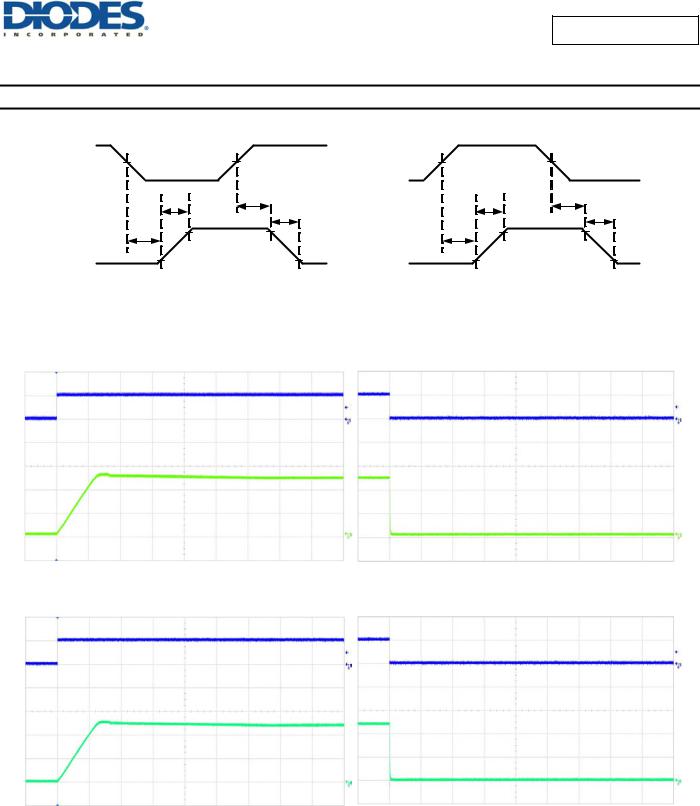
Figure 1 Voltage Waveforms: AP2182 (left), AP2192 (right)
All Enable Plots are for AP2192 Active High
Channel 1 Turn-On Delay and Rise Time |
Channel 1 Turn-Off Delay and Fall Time |
Ven 1 5V/div
Vout 1 2V/div
Ven 1 5V/div
Vout 1 |
CL= 1µF |
|
TA = +25°C |
||
2V/div |
||
CL = 1µF |
RL = 5Ω |
|
|
||
TA = +25°C |
|
|
RL = 5Ω |
|
|
400µs/div |
400µs/div |
|
Channel 2 Turn-On Delay and Rise Time |
Channel 2 Turn-Off Delay and Fall Time |
Ven 2 5V/div
Vout 2 2V/div
|
Ven 2 |
|
5V/div |
|
Vout 2 |
|
2V/div |
|
CL=1µF |
|
TA = +25°C |
|
RL = 5Ω |
400µs/div |
400µs/div |
CL=1µF TA=25°C RL=5Ω
AP2182/ AP2192 |
5 of 17 |
April 2013 |
Document number: DS31569 Rev. 7 - 2 |
www.diodes.com |
© Diodes Incorporated |

AP2182/ AP2192
Typical Performance Characteristics (cont.)
Channel 1 Turn-On Delay and Rise Time |
Channel 1 Turn-Off Delay and Fall Time |
Ven 2 |
Ven 2 |
|
|
5V/div |
5V/div |
|
|
|
|
CL = 100µF |
|
Vout 2 |
Vout 2 |
TA = +25°C |
|
RL = 5Ω |
|||
2V/div |
2V/div |
||
CL = 100µF |
|
|
|
TA = +25°C |
|
|
|
RL = 5Ω |
|
|
|
400µs/div |
|
400µs/div |
|
|
|
||
Channel 2 Turn-On Delay and Rise Time |
|
Channel 2 Turn-Off Delay and Fall Time |
Ven 2 |
Ven 2 |
|
|
5V/div |
5V/div |
|
|
|
|
CL = 100µF |
|
Vout 2 |
Vout 2 |
TA = +25°C |
|
RL = 5Ω |
|||
2V/div |
2V/div |
||
|
CL = 100µF |
|
|
|
TA = +25°C |
|
|
|
RL = 5Ω |
|
|
400µs/div |
|
400µs/div |
Ven 1 5V/div
Iout 1 500mA/div
Channel 1 Short Circuit Current, |
Channel 2 Short Circuit Current, |
Device Enabled Into Short |
Device Enabled Into Short |
Ven 2 5V/div
|
Iout 2 |
|
500mA/div |
|
VIN = 5V |
|
TA = 25°C |
|
CL = 68µF |
500µs/div |
500µs/div |
VIN = 5V TA = +25°C CL = 68µF
AP2182/ AP2192 |
6 of 17 |
April 2013 |
Document number: DS31569 Rev. 7 - 2 |
www.diodes.com |
© Diodes Incorporated |
 Loading...