


AL9910
A
Description
L9910/ AL9910A/ AL9910-5/AL9910A-5
UNIVERSAL HIGH VOLTAGE HIGH BRIGHTNESS LED DRIVER
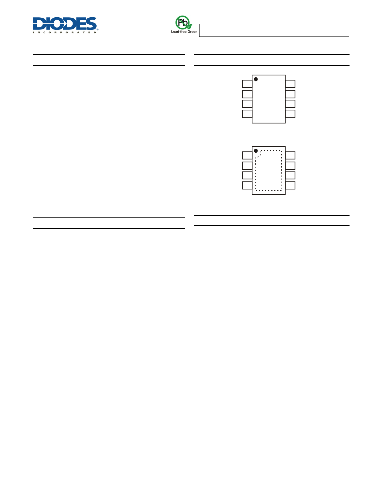
Pin Assignments
IN
IN
(Top View)
1
2
AL9910
3
4
SO-8
(Top View)
1
2
AL9910
3
4
SO-8EP
R
8
OSC
7
LD
V
6
DD
5
PWM_D
R
8
OSC
7
LD
V
6
DD
5
PWM_D
The AL9910/A high voltage PWM LED driver-controller provides an
efficient solution for offline high brightness LED lamps from rectified
line voltages ranging from 85V
external MOSFETs at switching frequencies up to 300kHz, with the
switching frequency determined by a single resistor. The AL9910
topology creates a constant current through the LEDs providing
constant light output. The output current is programmed by one
external resistor and is ultimately determined by the external
MOSFET chosen and therefore allows many low current LEDs to be
driven as well as a few high current LEDs.
The LED brightness can be varied by both Linear and PWM dimming
using the AL9910’s LD and PWM_D pins respectively. The PWM_D
input operates with duty ratio of 0-100% and frequency of up to
several kHz.
The AL9910 can withstand input voltages up to 500V which makes it
very resilient to transients at standard mains voltages. As well as
standard SO-8 package the AL9910 is available in the thermally
enhanced SO-8EP package.
Features
• >90% Efficiency
• Universal Rectified 85 to 277V
• Input Voltage Up to 500V
• Internal Voltage Regulator Removes Start-Up Resistor
7.5V MOSFET Drive – AL9910
10V MOSFET Drive – AL9910A
• Tighter Current Sense Tolerance: 5% AL9910-5, AL9910A-5
• Drives LED Lamps with Both High and Low Current LEDs
• LED Brightness Control with Linear and PWM Dimming
• Internal Thermal Protection (OTP)
• Available in SO-8 and SO-8EP Packages
• Totally Lead-Free & Fully RoHS Compliant (Notes 1 & 2)
• Halogen and Antimony Free. “Green” Device (Note 3)
Notes: 1. No purposely added lead. Fully EU Directive 2002/95/EC (RoHS) & 2011/65/EU (RoHS 2) compliant.
2. See http://www.diodes.com/quality/lead_free.html for more information about Diodes Incorporated’s definitions of Halogen- and Antimony-free, "Green"
and Lead-free.
3. Halogen- and Antimony-free "Green” products are defined as those which contain <900ppm bromine, <900ppm chlorine (<1500ppm total Br + Cl) and
<1000ppm antimony compounds.
up to 277VAC. The AL9910 drives
AC
Input Range
AC
Applications
• LED Offline Lamps
• High Voltage DC-DC LED Driver
• Signage and Decorative LED Lighting
• Back Lighting of Flat Panel Displays
• General Purpose Constant Current Source
V
CS
GND
GATE
V
CS
GND
GATE
AL9910/ AL9910A/ AL9910-5/ AL9910-5A
Document number: DS35103 Rev. 9 - 2
1 of 15
www.diodes.com
May 2014
© Diodes Incorporated
A
L9910/ AL9910A/ AL9910-5/AL9910A-5
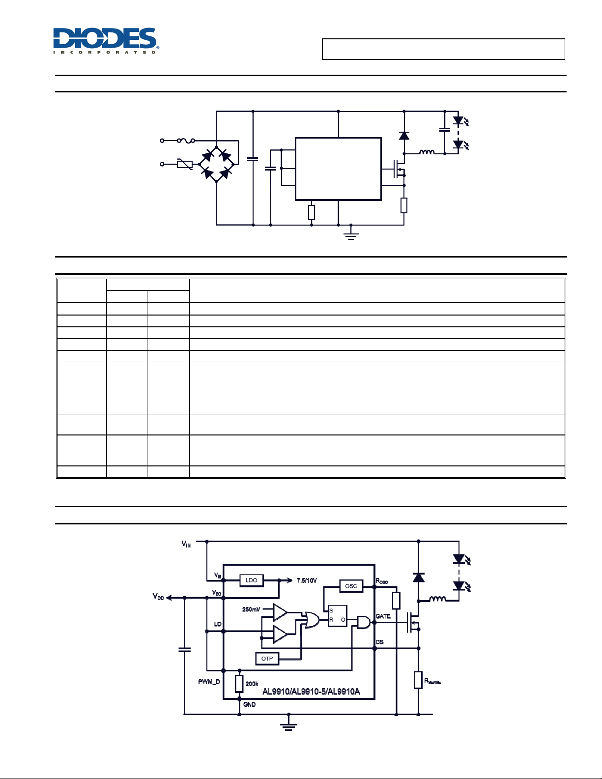
Typical Applications Circuit
C3
C3
D1
VACIN
VACIN
BR1
BR1
C1
C1
C2
C2
V
V
LD
LD
PWM_D
PWM_D
R
R
OSC
OSC
DD
DD
AL9910/A
AL9910/A
R
R
OSC
OSC
V
V
IN
IN
GND
GND
GATE
GATE
CS
CS
Q1
Q1
R
R
D1
SENSE
SENSE
L1
L1
Pin Descriptions
Pin
Name
VIN
SO-8 SO-8EP
Pin Number
1 1
Input Voltage
Function
CS 2 2 Senses LED string and external MOSFET switch current
GND 3 3 Device Ground
Gate 4 4 Drives the gate of the external MOSFET switch.
PWM_D 5 5 Low Frequency PWM Dimming pin, also Enable input. Internal 200kΩ pull-down to GND.
Internally regulated supply voltage.
7.5V nominal for AL9910 and AL9910-5
10V nominal for AL9910A.
VDD
6 6
Can supply up to 1 mA for external circuitry. A sufficient storage capacitor is used to provide storage when
the rectified AC input is near the zero crossing.
LD 7 7
Linear Dimming Input. Changes the current limit threshold at current sense comparator and changes the
average LED current.
Oscillator Control. A resistor connected between this pin and ground sets the PWM frequency. The devices
R
OSC
8 8
can be switched into constant off time (PFM) mode by connecting the external oscillator resistor between
pin and the gate of the external MOSFET.
R
OSC
EP PAD N/A EP Exposed Pad (bottom). Connect to GND directly underneath the package.
Functional Block Diagram
AL9910/ AL9910A/ AL9910-5/ AL9910-5A
Document number: DS35103 Rev. 9 - 2
2 of 15
www.diodes.com
May 2014
© Diodes Incorporated
A
L9910/ AL9910A/ AL9910-5/AL9910A-5
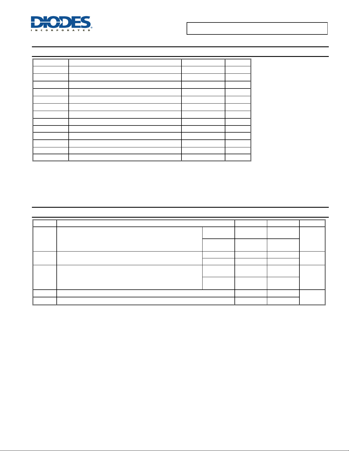
Absolute Maximum Ratings (Note 4) (@T
= +25°C, unless otherwise specified.)
A
Symbol Parameter Ratings Unit
V
Maximum input voltage, VIN, to GND
IN(MAX)
VCS
VLD
V
PWM_D
V
GATE
V
DD(MAX)
Maximum CS input pin voltage relative to GND -0.3 to +0.45 V
Maximum LD input pin voltage relative to GND
Maximum PWM_D input pin voltage relative to GND
Maximum GATE pin voltage relative to GND
Maximum VDD pin voltage relative to GND
Continuous Power Dissipation (T
SO-8 (derate 6.3mW/°C above +25°C)
= +25°C)
A
-0.5 to +520 V
-0.3 to (VDD +0.3)
-0.3 to (VDD +0.3)
-0.3 to (VDD +0.3)
12 V
630 mW
V
V
V
SO-8EP (derate at 22mW/°C above 25°C) 2200 mW
TJ
TST
Junction Temperature Range +150 °C
Storage Temperature Range -65 to +150 °C
ESD HBM Human Body Model ESD Protection (Note 5) 1500 V
ESD MM Machine Model ESD Protection (Note 5) 300 V
Notes: 4. Stresses above those listed under Absolute Maximum Ratings may cause permanent damage to the device. This is a stress rating only; functional
operation of the device at these or any other conditions above those listed in the operational sections of this specification is not implied. Exposure
to absolute maximum rating conditions for extended periods may affect device reliability.
All voltages are with respect to Ground. Currents are positive into, negative out of the specified terminal.
5. Semiconductor devices are ESD sensitive and may be damaged by exposure to ESD events. Suitable ESD precautions should be taken when
handling and transporting these devices
Recommended Operating Conditions (@T
= +25°C, unless otherwise specified.)
A
Symbol Parameter Min Max Unit
AL9910
V
Input DC Supply Voltage Range
INDC
AL9910-5
AL9910A
Al9910A-5
Ambient Temperature Range (Note 6)
TA
AL9910_S
AL9910_SP -40 +105
AL9910
VDD Maximum Recommended Voltage Applied to VDD Pin (Note 7)
AL9910-5
AL9910A
AL9910A-5
V
EN(LO)
V
Notes: 6. Maximum ambient temperature range is limited by allowable power dissipation. The Exposed pad SO-8EP with its lower thermal impedance allows
the variants using this package to extend the allowable maximum ambient temperature range.
7. When using the AL9910 in isolated LED lamps an auxiliary winding might be used.
Pin PWM_D Input Low Voltage
Pin PWM_D Input High Voltage
EN(HI)
15.0 500
20.0 500
-40 +85
10
12
0 1
2.4
VDD
V
°C
V
V
AL9910/ AL9910A/ AL9910-5/ AL9910-5A
Document number: DS35103 Rev. 9 - 2
3 of 15
www.diodes.com
May 2014
© Diodes Incorporated
A
L9910/ AL9910A/ AL9910-5/AL9910A-5
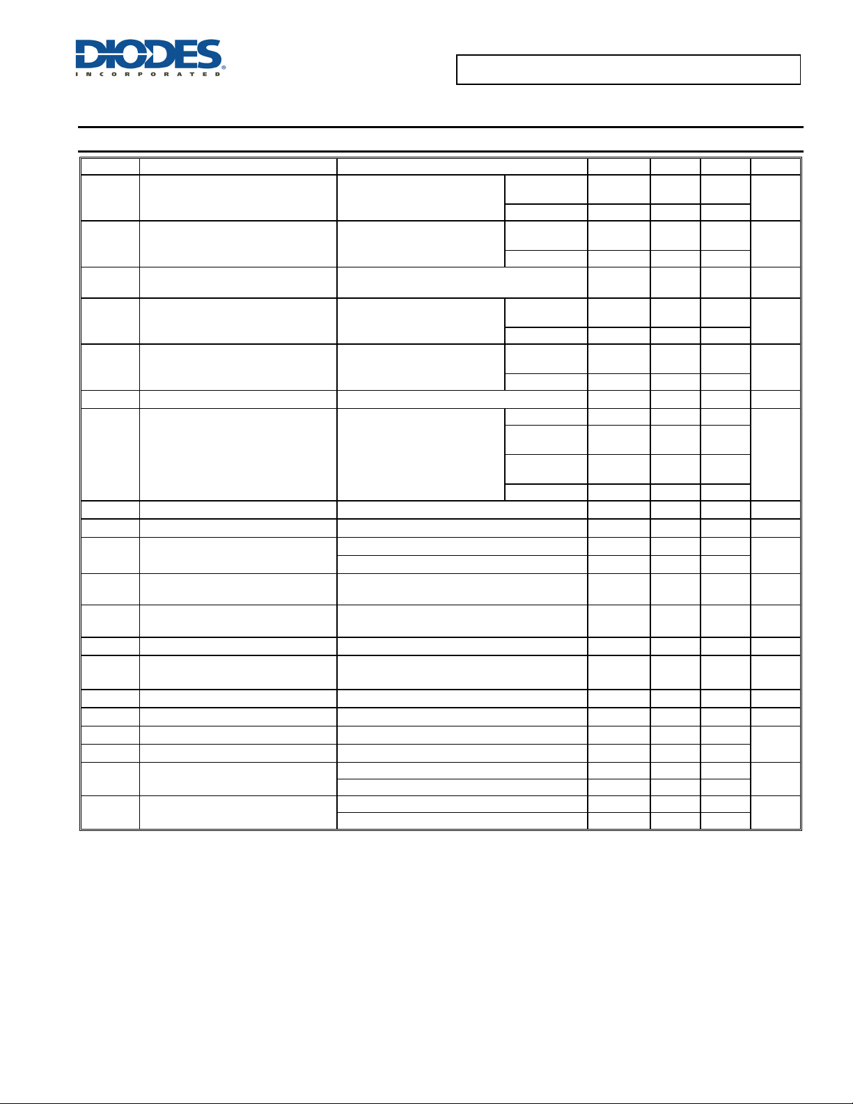
Electrical Characteristics (@T
= +25°C, unless otherwise specified.)
A
Symbol Parameter Conditions Min Typ Max Unit
I
INSD
VDD
I
DD(ext)
UVLO
Shut-Down Mode Supply Current
Internally Regulated Voltage
Current Available for External
V
DD
Circuitry
V
Under Voltage Lockout Threshold V
DD
Pin PWM_D to GND,
V
IN
V
IN
l
DD(ext)
V
IN
DD
= V
= V
= V
rising
(Note 6)
IN(MIN)
~500V, (Note 8)
IN(MIN)
= 0, Gate pin open
to 100V (Notes 8 & 9)
IN(MIN)
AL9910
AL9910-5
AL9910A
AL9910
AL9910-5
AL9910A 9 10 11
AL9910
AL9910-5
0.50 1
0.65
1.2
7.0 7.5 8.0
1.0 mA
6.4 6.7 7
mA
V
V
AL9910A 8 9 10
∆UVLO
V
Under Voltage Lockout Hysteresis V
DD
falling
DD
AL9910
AL9910-5
500
mV
AL9910A 750
R
PWM_D
V
CS(HI)
PWM_D Pull-Down Resistance
Current Sense Threshold Voltage
V
= 5V
PWM_D
Full ambient temperature range
(Note 10)
AL9910
AL9910A
AL9910A-5
150 200 250 kΩ
225 250 275
230 255 280
mV
242 255 267
AL9910-5 237.5 250 262.5
V
GATE(HI)
V
GATE(LO)
f
D
t
BLANK
t
DELAY
t
t
T
Notes: 8. V
9. Also limited by package power dissipation limit, whichever is lower.
10. Full ambient temperature range for AL9910-5S, AL9910AS and AL9910S is -40 to +85°C; for AL9910-5SP, AL9910ASP and AL9910SP is
-40°C to +105°C.
11. Device mounted on FR-4 PCB (25mm x 25mm 1oz copper, minimum recommended pad layout on top. For better thermal performance, larger
copper pad for heat-sink is needed.
12. Device mounted on FR-4 PCB (51mm x 51mm 2oz copper, minimum recommended pad layout on top layer and thermal vias to bottom layer ground
plane. For better thermal performance, larger copper pad for heat-sink is needed.
GATE High Output Voltage
GATE Low Output Voltage
Oscillator Frequency
OSC
Maximum Oscillator PWM Duty Cycle
MAXhf
Linear Dimming Pin Voltage Range
VLD
Current Sense Blanking Interval
Delay From CS Trip to GATE lo
GATE Output Rise Time
RISE
GATE Output Fall Time
FALL
Thermal Shut Down
TSD
Thermal Shut Down Hysteresis
SDH
Thermal Resistance Junction-to-
θJA
Ambient
Thermal Resistance Junction-to-Case
θJC
for the AL9910 is 15V and for the AL9910A it is 20V.
IN(MIN)
I
= 10mA VDD -0.3
OUT
I
= -10mA
OUT
R
= 1MΩ
OSC
R
= 226kΩ
OSC
= 25kHz, at GATE,
f
PWMhf
CS to GND.
Full ambient temperature range (Note 10),
V
= 20V
IN
VCS = 0.45V, VLD = VDD
V
= 20V, VLD = 0.15,
IN
= 0 to 0.22V after T
V
CS
C
= 500pF
GATE
C
= 500pF
GATE
BLANK
0 0.3 V
20 25 30
80 100 120
100 %
0
160 250 440 ns
300 ns
30 50 ns
30 50 ns
150
50
SO-8 (Note 11) 110
SO-8EP (Note 12) 66
SO-8 (Note 11)
22
SO-8EP (Note 12) 9
VDD
-
250 mV
V
kHz
°C
°C/W
°C/W
AL9910/ AL9910A/ AL9910-5/ AL9910-5A
Document number: DS35103 Rev. 9 - 2
4 of 15
www.diodes.com
May 2014
© Diodes Incorporated
A
5
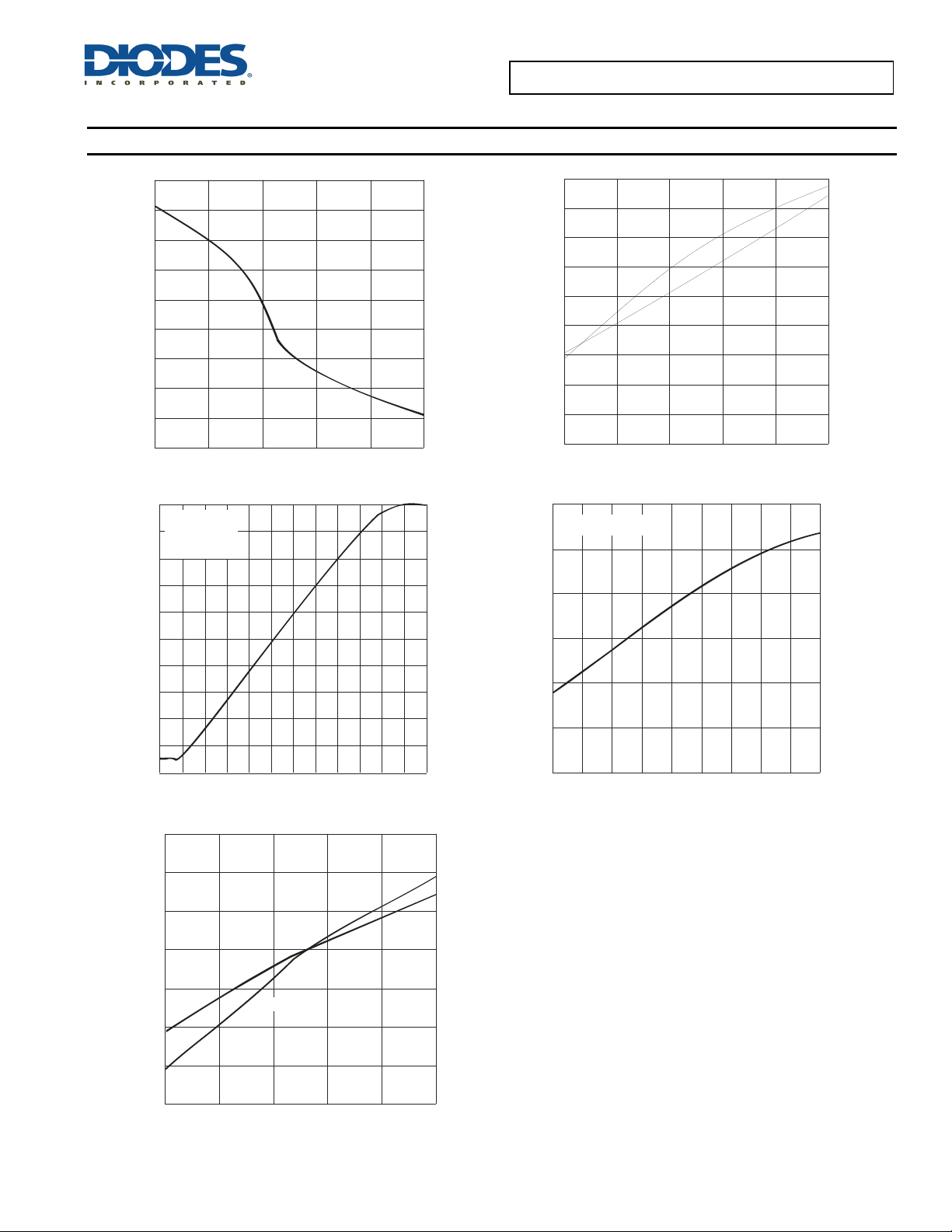
Typical Characteristics
3.0
2.5
2.0
L9910/ AL9910A/ AL9910-5/AL9910A-5
460
440
V = 400V
420
IN
1.5
1.0
0.5
0.0
-0.5
CURRENT SENS E THRESHOLD (mV)
-1.0
-1.5
-40 -15 10 35 60 85
AMBIE NT TEMP ER ATURE (°C)
Change in Current Sense Thresho ld vs. Ambient Temperatu re
100
I = 281mA
LED
90
V = 264V
IN
T = 23.5C
A
80
70
60
50
OUT MAX
I (%)
40
30
20
10
0
050
100 150 200 250 300
V DIMMING CONTROL (mV)
LD
I vs. V Dimming Control
OUT MAX LD
1.
400
V = 15V
IN
380
360
340
INPUT CURRENT (µA)
320
300
280
-40 -15 10 35 60 85
AMBIEN T TE MPE RATURE ( C)
°
Input Current vs. Ambient Temperatu re
450
I = 180mA
LED(NOM )
400
350
300
250
200
SHORT CIRCUIT OUTPUT CURRE NT (mA)
150
85 10 5 12 5 145 165 185 205 22 5
I NPUT V OLTAG E (V )
RMS
180mA LED Driver Short Ci rcu it Out put Current vs. I nput Voltage
245 26 5
1.0
0.5
0.0
R = 226k
OSC
Ω
-0.5
R = 1M
Ω
OSC
-1.0
CHANGE IN FREQUENCY (%)
-1.5
-2.0
-40 -15 10 35 60 85
AMBIE NT TEMPER ATURE ( °C)
Chan ge in Os cill ation Frequency vs. Ambie nt Temp erature
AL9910/ AL9910A/ AL9910-5/ AL9910-5A
Document number: DS35103 Rev. 9 - 2
5 of 15
www.diodes.com
May 2014
© Diodes Incorporated
 Loading...