


Diodes AP2301FGEG, AP2301SN, AP2311FGEG, AP2311SN, AP2301M8G Schematic [ru]
...AP2301/AP2311
2.0A SINGLE CHANNEL CURRENT-LIMITED POWER SWITCH
Description
The AP2301 and AP2311 are single channel current-limited integrated high-side power switches optimized for Universal Serial Bus (USB) and other hot-swap applications. The family of devices complies with USB standards and is available with both polarities of Enable input.
The devices have fast short-circuit response time for improved overall system robustness, and have integrated output discharge function to ensure completely controlled discharging of the output voltage capacitor. They provide a complete protection solution for applications subject to heavy capacitive loads and the prospect of short circuit, and offer reverse current blocking, over-current, over-temperature and short-circuit protection, as well as controlled rise time and undervoltage lockout functionality. A 7ms deglitch capability on the opendrain Flag output prevents false over-current reporting and does not require any external components.
All devices are available in SO-8, MSOP-8, MSOP-8EP, U-DFN3030- 8 and U-DFN2020-6 packages.
Features
Pin Assignments
|
|
|
|
( Top View ) |
|
|
|
||||
|
|
|
|
|
|
|
|
|
|
|
|
|
|
|
|
|
|
|
|
|
|
|
|
GND |
1 |
|
|
|
|
8 |
|
NC |
|
||
|
IN |
|
|
|
|
|
|
|
OUT |
|
|
|
2 |
|
|
|
|
7 |
|
|
|||
|
|
|
|
|
|
|
|
|
OUT |
|
|
|
IN |
3 |
|
|
|
|
6 |
|
|
||
|
EN |
|
|
|
|
|
|
|
FLG |
|
|
|
4 |
|
|
|
|
5 |
|
|
|||
|
|
|
|
|
|
|
|
|
|
|
|
|
|
|
|
|
SO-8 |
|
|
|
|||
|
|
|
|
( Top View ) |
|
|
|
||||
GND |
|
|
|
|
|
|
|
|
|
|
NC |
1 |
|
|
|
|
|
|
|
||||
|
|
|
|
|
|
|
8 |
|
|||
|
|
|
|
|
|
|
|
|
|||
|
|
|
|
|
|
|
|
||||
IN |
|
|
|
|
|
|
|
|
|
|
OUT |
|
|
|
|
|
|
|
|
|
|
||
2 |
|
|
|
|
|
|
|
7 |
|||
IN |
|
|
|
|
|
|
|
|
|
|
OUT |
|
|
|
|
|
|
|
|
|
|
||
3 |
|
|
|
|
|
|
|
6 |
|
||
EN |
|
|
|
|
|
|
|
|
|
|
FLG |
|
|
|
|
|
|
|
|
|
|
||
|
|
|
|
|
|
|
|
|
|
||
4 |
|
|
|
|
|
|
|
||||
|
|
|
|
|
|
|
5 |
|
|||
MSOP-8 /MSOP-8EP Note: latter with exposed pad
(dotted line)
(Top View)
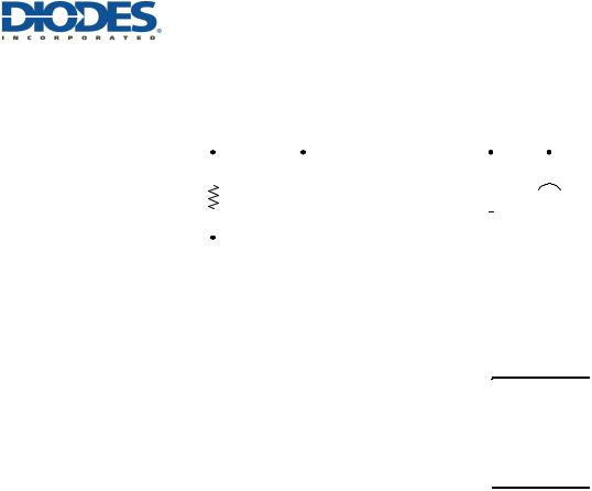
•Single channel current-limited power switch
•Output discharge function
•Fast short-circuit response time: 2µs
•2.5A accurate current limiting
•Reverse current blocking
•70mΩ on-resistance
•Input voltage range: 2.7V - 5.5V
•Built-in soft-start with 0.6ms typical rise time
•Over-current and thermal protection
•Fault report (FLG) with blanking time (7ms typ)
•ESD protection: 2kV HBM, 200V MM
•Ambient temperature range: -40°C to +85°C
•SO-8, MSOP-8, MSOP-8EP, U-DFN3030-8 and U-DFN2020-6: Available in “Green” Molding Compound (No Br, Sb)
GND |
1 |
|
|
|
|
8 |
NC |
|
|
|
|||||||
|
|
|
|
|
|
|
|
|
IN |
2 |
|
|
|
7 |
OUT |
||
|
|
|
|
|
|
|
|
|
IN |
3 |
6 |
OUT |
EN |
|
|
|
|
|
4 |
|
5 FLG |
|||
|
|||||
|
|
|
|
|
|
U-DFN3030-8 Type E
Totally Lead-free & Fully RoHS Compliant (Notes 1 & 2) |
U-DFN2020-6 |
|
Halogen and Antimony Free. “Green” Device (Note 3) |
||
|
||
• UL Recognized, File Number E322375 |
|
|
• IEC60950-1 CB Scheme Certified |
Applications |
|
|
||
|
• LCD TVs & Monitors |
|
|
• Set-Top-Boxes, Residential Gateways |
|
|
• Laptops, Desktops, Servers, e-Readers, Printers, Docking |
|
|
Stations, HUBs |
Notes: |
1. |
No purposely added lead. Fully EU Directive 2002/95/EC (RoHS) & 2011/65/EU (RoHS 2) compliant. |
|
2. |
See http://www.diodes.com/quality/lead_free.html for more information about Diodes Incorporated’s definitions of Halogenand Antimony-free, "Green" |
|
|
and Lead-free. |
|
3. |
Halogenand Antimony-free "Green” products are defined as those which contain <900ppm bromine, <900ppm chlorine (<1500ppm total Br + Cl) and |
|
|
<1000ppm antimony compounds. |
AP2301/AP2311 |
1 of 18 |
February 2014 |
Document number: DS32241 Rev. 5 - 2 |
www.diodes.com |
© Diodes Incorporated |
|
|
|
|
|
|
|
|
|
|
|
|
|
|
|
|
|
|
|
|
|
|
|
|
|
|
|
|
|
|
|
|
|
|
|
|
|
|
|
|
|
|
|
|
|
|
|
|
AP2301/AP2311 |
|
|
|
|
|
|
|
|
|
|
|
|
|
|
|
|
|
|
|
|
|
|
|
|
|
|
|
|
|
|
|
|
|
|
|
|
|
|
|
|
|
|
|
|
|
|
|
|
|||
|
Typical Applications Circuit |
|
|
|
|
|
|
|
|
|
|
|
|
|
|
|
|
|
|
|
|
|
|
|
|
|
|
|
|
|
|
|
|
|
|
|
|
|
|
||||||||||
|
|
|
|
|
Enable Active High |
|
|
|
|
|
|
|
|
|
|
|
|
|
|
|
|
|
|
|
|
|
|
|
|
|
|
|
|
|
|
|
|
|
|||||||||||
|
|
|
|
|
|
|
|
|
IN |
|
|
|
|
|
|
|
OUT |
|
|
|
|
|
|
|
|
|
|
|
|
|
|
|
|
|
|
Load |
|
||||||||||||
|
|
|
Power Supply |
|
|
|
|
|
|
|
|
|
|
|
|
|
|
|
|
|
|
|
|
|
|
|
|
|
|
|
|
|
|
|
|
|
|
|
|
|
|
|
|||||||
|
|
|
|
|
|
|
|
|
|
|
|
|
|
|
|
|
|
|
|
|
|
|
|
|
|
|
|
|
|
|
|
|
|
||||||||||||||||
|
|
|
|
2.7V to 5.5V |
|
|
|
|
|
|
|
|
|
|
|
|
|
|
|
|
|
|
|
|
|
|
|
|
|
|
|
|
|
|
|
|
|
|
|
|
|
|
|
|
|
||||
|
|
|
|
|
|
|
|
|
|
|
|
|
|
|
|
|
|
|
|
|
|
|
|
|
|
|
|
|
|
|
|
|
|
|
|
|
|
|
|
|
|
|
|
|
|
|
|
|
|
|
|
|
|
|
|
|
|
|
|
10k |
|
|
|
|
|
0.1uF |
|
|
|
|
|
|
|
|
|
|
|
|
0.1uF |
|
|
|
|
|
|
120uF |
|
|
|||||||||||
|
|
|
|
|
|
|
|
|
|
|
|
|
|
|
|
|
|
|
|
|
|
|
|
|
|
|
|
|
|
|
|
|
|
|
|
|
|
||||||||||||
|
|
|
|
|
|
|
|
|
|
|
|
|
|
|
|
|
|
|
|
|
FLG |
|
|
|
|
|
|
|
|
|
|
|
|
|
|
|
|
|
|
|
|
|
|
|
|
|
|
|
|
|
|
|
|
|
|
|
|
|
|
|
|
|
|
|
|
|
|
|
|
|
|
|
|
|
|
|
|
|
|
|
|
|
|
|
|
|
|
|
|
|
|
|
|
|
|
|
|
|
|
|
|
|
|
|
|
|
|
|
|
|
|
|
|
|
|
|
|
|
|
|
|
|
|
|
|
|
|
|
|
|
|
|
|
|
|
|
|
|
|
|
|
|
|
|
|
|
|
|
|
|
|
|
|
|
|
|
|
|
|
|
|
|
|
|
|
|
|
|
|
|
|
|
|
|
|
|
|
|
|
|
|
|
|
|
|
|
|
|
|
|
|
|
|
|
|
|
|
|
|
|
|
|
|
|
|
|
|
|
|
|
|
|
|
|
|
|
|
|
|
|
EN |
GND |
|
|
|
|
|
|
|
|
|
|
|
|
|
|
|
|
|
|
|
|
|||||||
|
|
|
|
|
|
|
|
|
|
|
|
|
|
ON |
|
|
|
|
|
|
|
|
|
|
|
|
|
|
|
|
|
|
|
|
|
|
|
|
|||||||||||
|
|
|
|
|
|
|
|
|
|
|
|
|
|
|
|
|
|
|
|
|
|
|
|
|
|
|
|
|
|
|
|
|
|
|
|
|
|
|
|
|
|
|
|
|
|
|
|||
|
|
|
|
|
|
|
|
|
|
|
|
|
|
|
|
|
|
|
|
|
|
|
|
|
|
|
|
|
|
|
|
|
|
|
|
|
|
|
|
|
|
|
|
|
|||||
|
|
|
|
|
|
|
|
|
|
|
|
OFF |
|
|
|
|
|
|
|
|
|
|
|
|
|
|
|
|
|
|
|
|
|
|
|
|
|
|
|
|
|
|
|
|
|
|
|||
|
Available Options |
|
|
|
|
|
|
|
|
|
|
|
|
|
|
|
|
|
|
|
|
|
|
|
|
|
|
|
|
|
|
|
|
|
|
|
|
|
|
|
|
|
|
|
|
|
|||
|
|
|
|
|
|
|
|
|
|
|
|
|
|
|
|
|
|
|
|
|
|
|
|
|
|
|
|
|
|
|
|
|
|
|
|
|
|
|
|
|
|
|
|
|
|
||||
|
|
|
|
|
|
|
|
|
|
|
|
|
|
|
|
|
|
|
|
|
|
|
|
|
|
|
|
|
|
|
|
|
|
|
|
|
|
|
|
|
|
|
|
|
|
||||
|
Part Number |
|
Channel |
|
|
Enable Pin (EN) |
|
|
|
Recommended Maximum |
|
Typical Current |
|
Package |
|||||||||||||||||||||||||||||||||||
|
|
|
|
|
Continuous Load Current (A) |
|
|
Limit (A) |
|
|
|
||||||||||||||||||||||||||||||||||||||
|
|
|
|
|
|
|
|
|
|
|
|
|
|
|
|
|
|
|
|
|
|
|
|
||||||||||||||||||||||||||
|
AP2301 |
|
|
1 |
|
|
|
Active Low |
|
|
|
|
|
|
|
|
|
|
|
|
|
|
|
|
|
|
|
|
|
|
|
|
|
|
|
|
|
|
|
SO-8 |
|||||||||
|
|
|
|
|
|
|
|
|
|
|
|
|
|
|
|
|
|
|
|
|
|
|
|
|
|
|
|
|
|
|
|
|
|
|
|
|
MSOP-8 |
||||||||||||
|
|
|
|
|
|
|
|
|
|
|
|
|
|
|
|
|
|
|
|
|
|
|
|
|
|
|
|
|
|
|
|
|
|
|
|
|
|
|
|
|
|
|
|
|
|
|
|
||
|
|
|
|
|
|
|
|
|
|
|
|
|
|
|
|
|
|
|
|
|
|
|
2A |
|
|
|
2.5A |
|
MSOP-8EP |
||||||||||||||||||||
|
|
|
|
|
|
|
|
|
|
|
|
|
|
|
|
|
|
|
|
|
|
|
|
|
|
|
|
|
|||||||||||||||||||||
|
AP2311 |
|
|
1 |
|
|
|
Active High |
|
|
|
|
|
|
|
|
|
|
|
|
|
|
|
|
|
|
|
|
|
|
|
|
|
|
|
|
|
|
|
U-DFN3030-8 |
|||||||||
|
|
|
|
|
|
|
|
|
|
|
|
|
|
|
|
|
|
|
|
|
|
|
|
|
|
|
|
|
|
|
|
|
|
|
|
|
U-DFN2020-6 |
||||||||||||
|
|
|
|
|
|
|
|
|
|
|
|
|
|
|
|
|
|
|
|
|
|
|
|
|
|
|
|
|
|
|
|
|
|
|
|
|
|
|
|
|
|
|
|
|
|
|
|
||
|
|
|
|
|
|
|
|
|
|
|
|
|
|
|
|
|
|
|
|
|
|
|
|
|
|
|
|
|
|
|
|
|
|
|
|
|
|
|
|
|
|
|
|
|
|||||
|
Pin Descriptions |
|
|
|
|
|
|
|
|
|
|
|
|
|
|
|
|
|
|
|
|
|
|
|
|
|
|
|
|
|
|
|
|
|
|
|
|
|
|
|
|
|
|||||||
|
|
|
|
|
|
|
|
|
|
|
|
|
|
|
|
|
|
|
|
|
|
|
|
|
|
|
|
|
|
|
|
|
|
|
|
|
|
|
|
|
|
|
|
|
|
||||
|
Pin |
|
|
|
|
Pin Number |
|
|
|
|
|
|
|
|
|
|
|
|
|
|
|
|
|
|
|
|
|
|
|
Function |
|
|
|||||||||||||||||
|
|
SO-8, |
|
MSOP-8EP, |
|
|
|
|
|
|
|
|
|
|
|
|
|
|
|
|
|
|
|
|
|
|
|
|
|
|
|||||||||||||||||||
|
Name |
|
|
|
U-DFN2020-6 |
|
|
|
|
|
|
|
|
|
|
|
|
|
|
|
|
|
|||||||||||||||||||||||||||
|
|
MSOP-8 |
U-DFN3030-8 |
|
|
|
|
|
|
|
|
|
|
|
|
|
|
|
|
|
|
|
|
|
|
|
|
|
|
|
|
|
|
||||||||||||||||
|
|
|
|
|
|
|
|
|
|
|
|
|
|
|
|
|
|
|
|
|
|
|
|
|
|
|
|
|
|
|
|
|
|
|
|
|
|
|
|
|
|
||||||||
|
GND |
|
1 |
|
1 |
|
|
|
|
|
2 |
|
|
|
|
|
Ground |
|
|
|
|
|
|
|
|
|
|
|
|
|
|
|
|
|
|
|
|
|
|
|
|
|
|
|
|
||||
|
IN |
|
2, 3 |
|
2, 3 |
|
|
|
1 |
|
|
|
|
|
Voltage Input Pin; Connect a 0.1µF or larger ceramic capacitor from IN to GND as |
||||||||||||||||||||||||||||||||||
|
|
|
|
|
|
|
|
|
|
|
|
|
|
close as possible. (all IN pins must be tied together externally) |
|||||||||||||||||||||||||||||||||||
|
|
|
|
|
|
|
|
|
|
|
|
|
|
|
|
|
|
|
|
||||||||||||||||||||||||||||||
|
EN |
|
4 |
|
4 |
|
|
|
|
|
3 |
|
|
|
|
|
Enable input, active low (AP2301) or active high (AP2311) |
|
|
||||||||||||||||||||||||||||||
|
FLG |
|
5 |
|
5 |
|
|
|
|
|
4 |
|
|
|
|
|
Over-temperature and over-current fault reporting with 7ms deglitch; active low open- |
||||||||||||||||||||||||||||||||
|
|
|
|
|
|
|
|
|
|
|
|
|
|
|
|
drain output. FLG is disabled for 7ms after turn-on. |
|
|
|||||||||||||||||||||||||||||||
|
|
|
|
|
|
|
|
|
|
|
|
|
|
|
|
|
|
|
|
|
|
||||||||||||||||||||||||||||
|
OUT |
|
6, 7 |
|
6, 7 |
|
|
|
5 |
|
|
|
|
|
Voltage Output Pin All OUT pins must be tied together externally. |
||||||||||||||||||||||||||||||||||
|
NC |
|
8 |
|
8 |
|
|
|
|
|
6 |
|
|
|
|
|
NC: |
|
|
|
|
|
|
|
|
|
|
|
|
|
|
|
|
|
|
|
|
|
|
|
|
|
|
|
|
||||
|
|
|
|
|
|
|
|
|
|
|
|
|
|
|
|
No Internal Connection; recommend tie to OUT pins |
|
|
|||||||||||||||||||||||||||||||
|
|
|
|
|
|
|
|
|
|
|
|
|
|
|
|
|
|
|
|
|
|
||||||||||||||||||||||||||||
|
Exposed |
|
— |
|
Exposed |
|
|
|
Exposed |
|
|
|
Exposed pad. |
|
|
|
|
|
|
|
|
|
|
|
|
|
|
|
|
|
|||||||||||||||||||
|
|
|
|
|
|
|
|
|
It should be externally connected to GND and thermal mass for enhanced thermal |
||||||||||||||||||||||||||||||||||||||||
|
Pad |
|
|
Pad |
|
|
|
|
Pad |
|
|
|
|||||||||||||||||||||||||||||||||||||
|
|
|
|
|
|
|
|
|
|
|
|
impedance. It should not be used as electrical ground conduction path. |
|||||||||||||||||||||||||||||||||||||
|
|
|
|
|
|
|
|
|
|
|
|
|
|
|
|
|
|
|
|
||||||||||||||||||||||||||||||
AP2301/AP2311 |
2 of 18 |
February 2014 |
Document number: DS32241 Rev. 5 - 2 |
www.diodes.com |
© Diodes Incorporated |
AP2301/AP2311
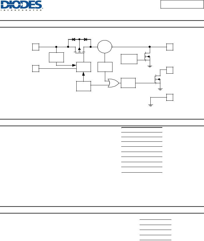
Functional Block Diagram
IN |
Current |
OUT |
|
Sense |
|||
|
|
UVLO |
|
|
Discharge |
|
|
|
|
Control |
|
EN |
Driver |
Current |
|
|
Limit |
FLG |
|||
|
||||
|
|
|
||
|
Thermal |
|
Deglitch |
|
|
|
|
||
|
Sense |
|
|
|
|
|
|
GND |
Absolute Maximum Ratings (@TA = +25°C, unless otherwise specified.)
Symbol |
Parameter |
|
Ratings |
Unit |
ESD HBM |
Human Body Model ESD Protection |
2 |
kV |
|
ESD MM |
Machine Model ESD Protection |
200 |
V |
|
VIN |
Input Voltage (Note 4) |
|
-0.3 to 6.5 |
V |
VOUT |
Output Voltage (Note 4) |
|
-0.3 to (VIN +0.3) or 6.5 |
V |
VEN , VFLG |
Enable Voltage (Note 4) |
|
-0.3 to (VIN +0.3) or 6.5 |
V |
ILOAD |
Maximum Continuous Load Current |
|
Internal Limited |
A |
TJ(MAX) |
Maximum Junction Temperature |
150 |
°C |
|
TST |
Storage Temperature Range (Note 5) |
|
-65 to +150 |
°C |
Notes: 4. All voltages referred to GND pin. Maximums are the lower of (VIN +0.3) and 6.5V
5.UL Recognized Rating from -30°C to +70°C (Diodes qualified TST from -65°C to +150°C)
Caution: Stresses greater than the 'Absolute Maximum Ratings' specified above, may cause permanent damage to the device. These are stress ratings only; functional operation of the device at these or any other conditions exceeding those indicated in this specification is not implied. Device reliability may be affected by exposure to absolute maximum rating conditions for extended periods of time.
Semiconductor devices are ESD sensitive and may be damaged by exposure to ESD events. Suitable ESD precautions should be taken when handling and transporting these devices.
Recommended Operating Conditions (@TA = +25°C, unless otherwise specified.)
Symbol |
Parameter |
Min |
Max |
Unit |
VIN |
Input voltage |
2.7 |
5.5 |
V |
IOUT |
Output Current |
0 |
2 |
A |
VIL |
EN Input Logic Low Voltage |
0 |
0.8 |
V |
VIH |
EN Input Logic High Voltage |
2 |
VIN |
V |
TA |
Operating Ambient Temperature |
-40 |
+85 |
°C |
AP2301/AP2311 |
3 of 18 |
February 2014 |
Document number: DS32241 Rev. 5 - 2 |
www.diodes.com |
© Diodes Incorporated |

AP2301/AP2311
Electrical Characteristics (@TA = +25°C, VIN = +5V, CIN = 0.1µF, CL = 1µF, unless otherwise specified.)
Symbol |
|
Parameter |
Test Conditions |
Min |
Typ |
Max |
Unit |
|
VUVLO |
|
Input UVLO |
VIN rising |
|
1.6 |
2.0 |
2.4 |
V |
∆VUVLO |
|
Input UVLO Hysteresis |
VIN decreasing |
|
|
50 |
|
mV |
ISHDN |
|
Input Shutdown Current |
Disabled, OUT = open |
|
|
0.1 |
1 |
µA |
IQ |
|
Input Quiescent Current |
Enabled, OUT = open |
|
|
60 |
100 |
µA |
ILEAK |
|
Input Leakage Current |
Disabled, OUT grounded |
|
|
0.1 |
1 |
µA |
IREV |
|
Reverse Leakage Current |
Disabled, VIN = 0V, VOUT = 5V, IREV at VIN |
|
0.01 |
1 |
µA |
|
|
|
|
VIN = 5V, IOUT= 2.0A |
TA = +25°C |
|
70 |
84 |
|
RDS(ON) |
|
Switch on-resistance |
-40°C ≤ TA ≤ +85°C |
|
|
105 |
mΩ |
|
|
|
|
|
|||||
|
VIN = 3.3V, IOUT = 2.0A |
TA = +25°C |
|
90 |
108 |
|||
|
|
|
|
|
||||
|
|
|
-40°C ≤ TA ≤ +85°C |
|
|
135 |
|
|
|
|
|
|
|
|
|
||
ILIMIT |
|
Over-Load Current Limit (Note 6) |
VIN = 5V, VOUT = 4.5V |
-40°C ≤ TA ≤ +85°C |
2.05 |
2.50 |
2.85 |
A |
ITrig |
|
Current limiting trigger threshold |
Output Current Slew rate (<100A/s) |
|
2.5 |
|
A |
|
ISHORT |
|
Short-Circuit Current Limit |
Enabled into short circuit |
|
|
2.75 |
|
A |
TSHORT |
|
Short-circuit Response Time |
VOUT = 0V to IOUT = ILIMIT (OUT shorted to ground) |
|
2 |
|
µs |
|
VIL |
|
EN Input Logic Low Voltage |
VIN = 2.7V to 5.5V |
|
|
|
0.8 |
V |
VIH |
|
EN Input Logic High Voltage |
VIN = 2.7V to 5.5V |
|
2 |
|
|
V |
ILEAK-EN |
|
EN Input leakage |
VIN = 5V, VEN = 0V and 5.5V |
|
|
0.01 |
1 |
µA |
ILEAK-O |
|
Output leakage current |
Disabled, VOUT = 0V |
|
|
0.5 |
1 |
µA |
TD(ON) |
|
Output turn-on delay time |
CL= 1µF, RLOAD = 5Ω |
|
|
0.1 |
|
ms |
TR |
|
Output turn-on rise time |
CL= 1µF, RLOAD = 5Ω |
|
|
0.6 |
1.5 |
ms |
TD(OFF) |
|
Output turn-off delay time |
CL= 1µF, RLOAD = 5Ω |
|
|
0.1 |
|
ms |
TF |
|
Output turn-off fall time |
CL= 1µF, RLOAD = 5Ω |
|
|
0.05 |
0.1 |
ms |
RFLG |
|
FLG output FET on-resistance |
IFLG = 10mA |
|
|
20 |
40 |
Ω |
IFOH |
|
FLG Off Current |
VFLG= 5V |
|
|
0.01 |
1 |
µA |
TBlank |
|
FLG blanking time |
Assertion or deassertion due to overcurrent and over- |
4 |
7 |
15 |
ms |
|
|
temperature condition |
|
||||||
|
|
|
|
|
|
|
|
|
TDIS |
|
Discharge time |
CL= 1µF, VIN = 5V, disabled to VOUT < 0.5V |
|
0.6 |
|
ms |
|
RDIS |
|
Discharge resistance (Note 7) |
VIN = 5V, disabled, IOUT= 1mA |
|
|
100 |
|
Ω |
TSHDN |
|
Thermal Shutdown Threshold |
Enabled |
|
|
140 |
|
°C |
THYS |
|
Thermal Shutdown Hysteresis |
|
|
|
20 |
|
°C |
|
|
|
SO-8 (Note 8) |
|
|
96 |
|
°C/W |
|
|
Thermal Resistance Junction-to- |
MSOP-8 (Note 8) |
|
|
130 |
|
°C/W |
θJA |
|
MSOP-8-EP (Note 9) |
|
|
92 |
|
°C/W |
|
|
|
Ambient |
|
|
|
|
|
|
|
|
U-DFN3030-8 (Note 9) |
|
|
84 |
|
°C/W |
|
|
|
|
|
|
|
|||
|
|
|
U-DFN2020-6 (Note 10) |
|
|
90 |
|
°C/W |
Notes: |
6. Pulse-testing techniques maintain junction temperature close to ambient temperature; thermal effects must be taken into account separately. |
|
||||||
7.The discharge function is active when the device is disabled (when enable is de-asserted or during power-up power-down when VIN < VUVLO). The discharge function offers a resistive discharge path for the external storage capacitor for limited time.
8.Device mounted on 2” x 2” FR-4 substrate PCB, 2oz copper, with minimum recommended pad layout.
9.Device mounted on 2” x 2” FR-4 substrate PCB, 2oz copper, with minimum recommended pad on top layer and thermal vias to bottom layer ground plane.
10.Device mounted on 1"x1" FR-4 substrate PCB, 2oz copper, with minimum recommended padon top layer and thermal vias to bottom layer ground.
AP2301/AP2311 |
4 of 18 |
February 2014 |
Document number: DS32241 Rev. 5 - 2 |
www.diodes.com |
© Diodes Incorporated |
|
|
|
|
|
|
|
AP2301/AP2311 |
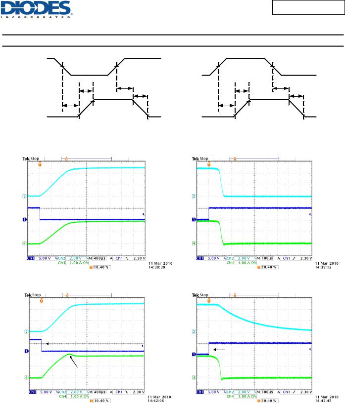
Typical Performance Characteristics |
|
|
|
|
|||
VEN |
50% |
|
50% |
VEN |
50% |
|
50% |
|
|
|
|
||||
|
|
TR |
TD(OFF) |
|
TR |
|
TD(OFF) |
|
|
TF |
|
|
TF |
||
|
|
|
|
|
|
||
|
TD(ON) |
90% |
90% |
|
TD(ON) |
90% |
90% |
|
|
|
|
||||
VOUT |
|
10% |
10% |
VOUT |
10% |
|
10% |
|
|
|
|
||||
|
|
Figure 1. Voltage Waveforms: AP2301 (left), AP2311 (right) |
|
|
|||
|
|
|
All Enable Plots are for Enable Active Low |
|
|
||
Turn-On Delay and Rise Time |
|
Turn-Off Delay and Fall Time |
|||||
VOUT |
|
|
TA=25°C |
VOUT |
|
|
TA=25°C |
|
|
V =5V |
2V/div |
|
|
VIN=5V |
|
2V/div |
|
|
IN |
|
|
|
|
|
|
CL=1uF |
|
|
|
CL=1uF |
|
VEN |
|
|
ROUT=2.5Ω |
VEN |
|
|
ROUT=2.5Ω |
|
|
|
|
|
|
||
5V/div |
|
|
|
5V/div |
|
|
|
 Device enabled
 Device disabled
IIN |
IIN |
|
1A/div |
||
1A/div |
||
|
|
Turn-On Delay and Rise Time |
|
Turn-Off Delay and Fall Time |
|
|
|
TA=25°C |
|
TA=25°C |
VOUT |
VIN=5V |
VOUT |
VIN=5V |
2V/div |
CL=120uF |
CL=120uF |
|
ROUT=2.5Ω |
|
2V/div |
|
||
ROUT=2.5Ω |
VEN |
|
|
|
|
||
|
Device enabled |
5V/div |
|
VEN |
|
Device disabled |
|
|
|
||
5V/div |
|
|
|
IIN |
Inrush current limit |
IIN |
|
1A/div |
|
||
|
|
1A/div |
|
AP2301/AP2311 |
5 of 18 |
February 2014 |
Document number: DS32241 Rev. 5 - 2 |
www.diodes.com |
© Diodes Incorporated |

AP2301/AP2311
Typical Performance Characteristics (cont.)
Device Enabled Into Short-Circuit
VEN |
TA=25°C |
|
VIN=5V |
||
5V/div |
||
CL=120uF |
||
|
||
|
ROUT=1Ω |
IOUT
1A/div
Full-Load to Short-Circuit
Transient Response
VOUT |
Output short |
TA=25°C |
2V/div |
circuited |
VIN=5V |
|
|
ROUT=2.5Ω |
IIN |
|
|
2A/div |
|
|
 Device turns off and re-enables into current limit
FLG 5V/div
No-Load to Short-Circuit
Transient Response
VOUT |
Output short |
TA=25°C |
|
2V/div |
|||
circuited |
VIN=5V |
||
|
ROUT=0Ω
IIN |
|
2A/div |
Device enters current limit |
|
|
FLG |
|
5V/div |
|
Inrush Current
VEN |
TA=25°C |
|
VIN=5V |
||
5V/div |
||
ROUT=2.5Ω |
||
|
CL=120uF CL=220uF
IOUT |
CL=470uF |
|
1A/div |
||
|
Short-Circuit to Full-Load
Recovery Response
Output short |
TA=25°C |
circuit removed |
|
VOUT |
VIN=5V |
2V/div |
ROUT=2.5Ω |
IIN |
Short circuit present and |
2A/div |
device thermal cycles |
FLG |
|
5V/div |
|
Short-Circuit to No-Load
Recovery Response
|
Output short |
|
VOUT |
circuit removed |
TA=25°C |
|
VIN=5V |
|
2V/div |
|
ROUT=0Ω |
IIN |
Short circuit present and |
|
2A/div |
device thermal cycles |
|
FLG 5V/div
AP2301/AP2311 |
6 of 18 |
February 2014 |
Document number: DS32241 Rev. 5 - 2 |
www.diodes.com |
© Diodes Incorporated |
 Loading...