


ANPEC APL5302-50KI-TR, APL5302-50KC-TR, APL5302-50D5I-TR, APL5302-50D5C-TR, APL5302-50BI-TR Datasheet
...
Low IQ, Low Dropout 300mA Fixed Voltage Regulator
Copyright ANPEC Electronics Corp.
Rev. A.9 -Apr., 2003
APL5301/2
www.anpec.com.tw1
ANPEC reserves the right to make changes to improve reliability or manufacturability without notice, and advise
customers to obtain the latest version of relevant information to verify before placing orders.
Features
The APL5301/2 series are micropower, low noise, low
dropout linear regulators, which operate from 3V to
6V input voltage and deliver up to 300mA. Typical output noise is just 60uV
RMS
with the addition of an external 0.33uF bypass capacitor in BP pin and typical
dropout voltage is only 260mV at 300mA loading. Designed for use in battery-powered system, the low 50uA
quiescent current makes it an ideal choice. Design
with an internal P-channel MOSFET pass transistor,
the APL5301/2 maintain a low supply current, independent of the load current and dropout voltage.
Other features include reverse current protection, ther-
mal-shutdown protection, current limit protection to
ensure specified output current and controlled short-
circuit current. The APL5301/2 regulators come in a
miniature SOP-8, SOT-23, SOT-23-5, SOT-89 and
SOT-89-5 packages.
Applications
• Notebook Computer
• PDA or Portable Equipments
• Noise-Sensitive Instrumentation Systems
••
••
• Low Noise : 60uV
RMS
(100Hz to 100kHz)
••
••
• Low Quiescent Current : 50uA (No load)
••
••
• Low Dropout Voltage : 400mV
(VOUT(Nominal)=3.0V Version @300mA)
••
••
• Very low Shutdown Current : < 0.5uA
••
••
• Fixed Output Voltage : 1.3V ~ 5.0V
by step 0.1V increment
••
••
• Stable with 1uF Output Capacitor
••
••
• Stable with Aluminum, Tantalum or Ceramic
Capacitors .
••
••
• Reverse Current Protection
••
••
• No Protection Diodes Needed
••
••
• Built in Thermal Protection
••
••
• Built in Current Limit Protection
••
••
• Controlled Short Circuit Current : 50mA
••
••
• Fast Transient Response
••
••
• Short Setting Time
••
••
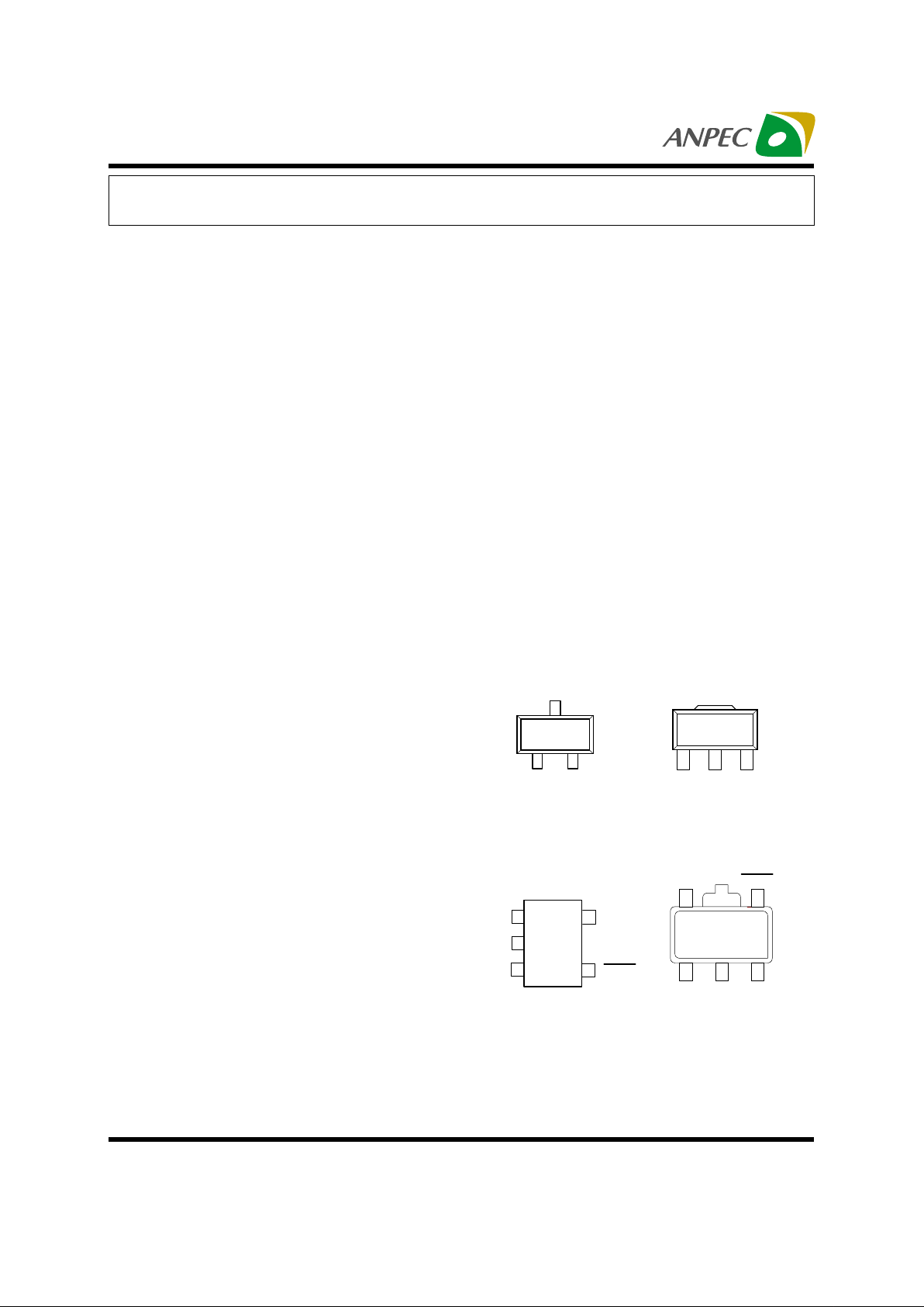
• SOP-8, SOT-23, SOT-23-5, SOT-89,
and SOT-89-5 Packages
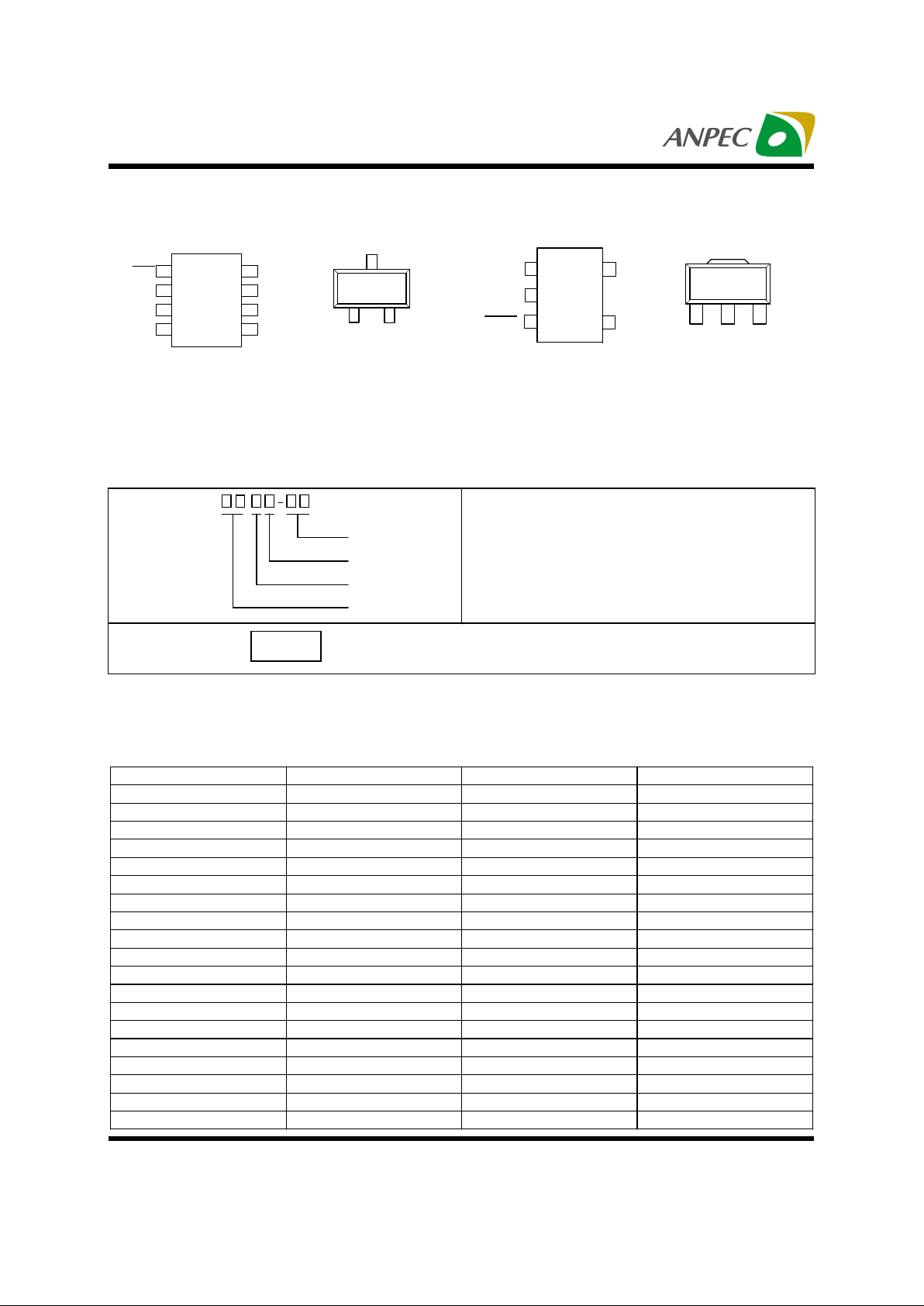
Pin Configuration
APL5301
SOT-89 (T op View)
GND
V
INVOUT
123
TAB is V
IN
SOT-23 (T op V iew)
GND
12
3
V
OUT
V
IN
APL5301
V
IN
GND
BP
V
OUT
1
2
3
5
SHDN
4
APL5301
SOT-23-5 (T op View)
APL5301
SOT-89-5 (T op View)
V
IN
GND
V
OUT
123
54
SHDNBP
GND
Copyright ANPEC Electronics Corp.
Rev. A.9 - Apr., 2003
APL5301/2
www.anpec.com.tw2
Package Code
A : S O T -23 B : S O T -2 3-5 D : SO T -89
D5 : SOT-89 -5 K : S O P -8
Temp . Range
C : 0 to 70 C I : -40 to 85 C
Handling Code
TR : Tape & Reel
Voltage Code :
13 : 1.3V ~ 34 : 3.4V 50 : 5.0V
APL5301/2 -
Handling Code
Temp . Range
Package Code
Voltage Code
APL5301/2
XXXXX 13
XXX XX - Date Code ; 13 - 1.3VAPL5301/2 -13 D/K :
Product Name Marking Product Name Marking
APL5301-13A/B 317X APL5302-13A/B 327X
APL5301-14A/B 318X APL5302-14A/B 328X
APL5301-15A/B 319X APL5302-15A/B 329X
APL5301-16A/B 31AX APL5302-16A/B 32AX
APL5301-17A/B 31BX APL5302-17A/B 32BX
APL5301-18A/B 31CX APL5302-18A/B 32CX
APL5301-19A/B 31DX APL5302-19A/B 32DX
APL5301-20A/B 31EX APL5302-20A/B 32EX
APL5301-21A/B 31FX APL5302-21A/B 32FX
APL5301-22A/B 31GX APL5302-22A/B 32GX
APL5301-23A/B 31HX APL5302-23A/B 32HX
APL5301-24A/B 31IX APL5302-24A/B 32IX
APL5301-25A/B 31JX APL5302-25A/B 32JX
APL5301-26A/B 31KX APL5302-26A/B 32KX
APL5301-27A/B 31LX APL5302-27A/B 32LX
APL5301-28A/B 31MX APL5302-28A/B 32MX
APL5301-29A/B 31NX APL5302-29A/B 32NX
APL5301-30A/B 31OX APL5302-30A/B 32OX
APL5301-31A/B 31PX APL5302-31A/B 32PX
Marking Information
SOT-23 and SOT-23-5 packages
V
IN
GND
BP
V
OUT
1
2
3
5
SHDN
4
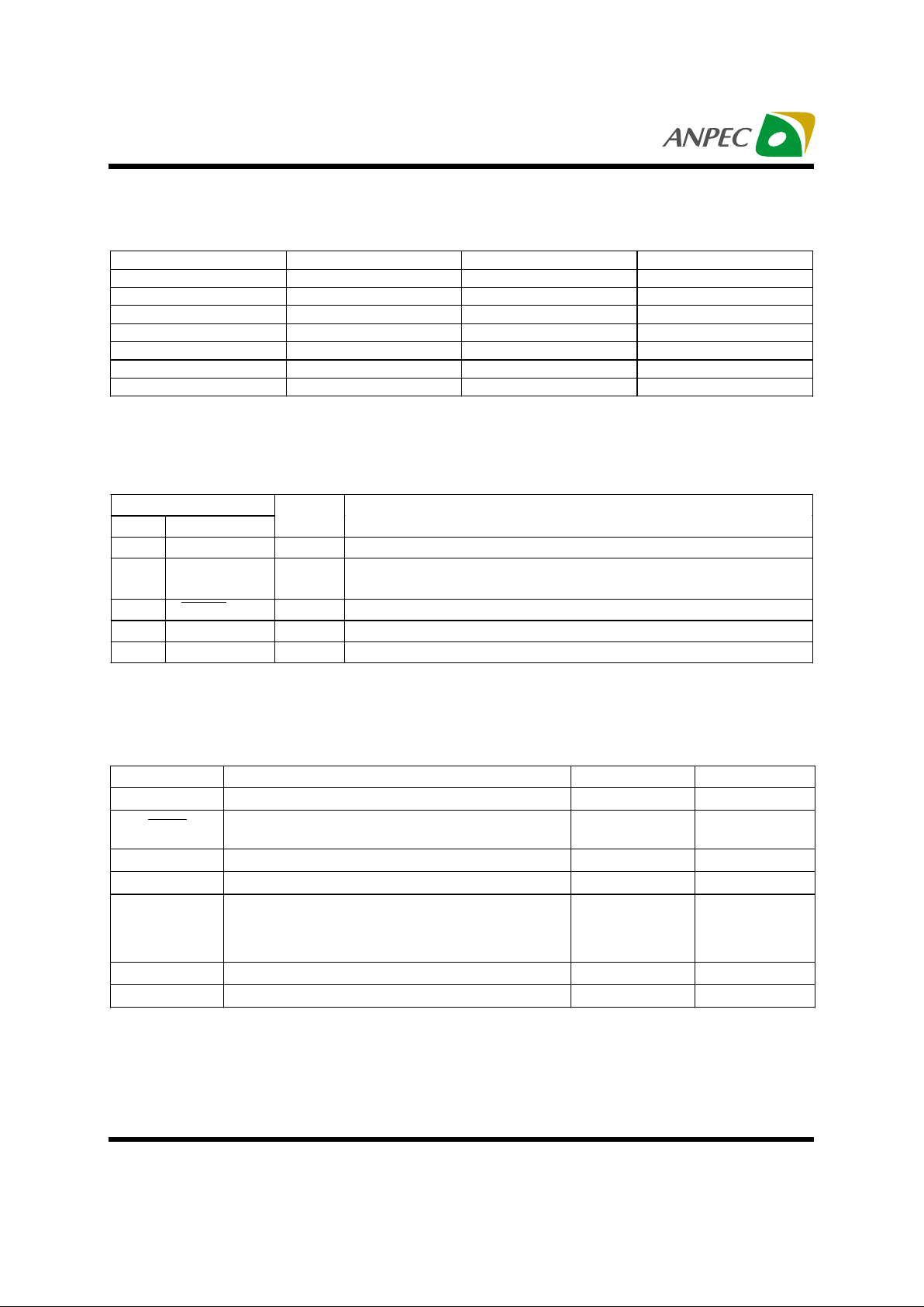
Pin Configuration (Cont.)
APL5302
SOT-89 (T op View)
SOT-23 (T op
View)
APL5302
Ordering and Marking Information
°°
SOP-8 (Top View)
1
2
3
45
6
7
8SHDN
V
IN
V
OUT
BP GND
GND
GND
GND
APL5301
GND V
IN
V
OUT
123
TAB is GND
GND
12
3
V
OUTVIN
SOT-23-5 (Top View)
APL5302
Copyright ANPEC Electronics Corp.
Rev. A.9 - Apr., 2003
APL5301/2
www.anpec.com.tw3
Product Name Marking Product Name Marking
APL5301-32A/B 31QX APL5302-32A/B 32QX
APL5301-33A/B 31RX APL5302-33A/B 32RX
APL5301-34A/B 31SX APL5302-34A/B 32SX
APL5301-35A/B 31TX APL5302-35A/B 32TX
APL5301-48A/B 31XX APL5302-48A/B 32XX
APL5301-49A/B 31YX APL5302-49A/B 32YX
APL5301-50A/B 31ZX APL5302-50A/B 32ZX
Marking Information (Cont.)
SOT-23 and SOT-23-5 packages
Pin Description
PIN
No. Name
I/O Description
1VINI Supply vol tage input.
2GND
Ground pins of the circuitry, and all ground pins must be soldered
To PCB with pr oper po w er dis sipa tion.
3 SHDN
(Note1)
I Shutdow n c o ntrol pin, low = off, high = n ro mal.
4BP
(Note1)
O Bypass signal pin of the regulator.
5V
OUT
O Output pin of the regulator.
Note1 : This pin does not exist in 3-pin package.
Symbol Parameter Rating Unit
VIN, V
OUT
Input Voltage or Out Voltage 6 V
SHDN
Shutdown Control Pin
6V
R
TH,JA
Thermal Resistance – Junction to Ambient 357 °C/W
P
D
Power Dissipation Internally Limited W
T
J
Operating Junction Temperature °C
Control Section 0 to 125
Power Transistor 0 to 150
T
STG
Storage Temperature Range -65 to +150 °C
T
L
Lead Temperature (Soldering, 10 second) 260 °C
Absolute Maximum Ratings
The last character “X” in the marking is for data code.
Copyright ANPEC Electronics Corp.
Rev. A.9 - Apr., 2003
APL5301/2
www.anpec.com.tw4
Electrical Characteristics
Unless otherwise noted these specifications apply over full temperature, VIN=3.8V, CIN=COUT=1uF, SHDN=VIN,
TJ=0 to 125°C. Typical values refer to TJ=25°C.
APL5301/2
Symbol Parameter Test Conditions
Min. Typ. Max.
Unit
VINInput Voltage 2.7 6 V
V
OUT
Output Voltage
V
OUT
+1.0V< VCC<6.0V, 0mA< I
OUT
V
OUT
-2
%
V
OUT
V
OUT
+2
%
V
I
LIMIT
Circuit Current Limit
V
IN=VOUT
+0.5V
500 mA
I
SHORT
Short Current V
OUT
=0V 50 mA
I
OUT
Load Current
V
IN=VOUT
+0.5V 300 mA
REG
LINE
Line Regulation
V
OUT
+0.5V< VCC<6.0V,
I
OUT
=150mA
410mV
REG
LOA
Load Regulation VIN =V
OUT
+0.5V, 0mA< I
OUT
< I
MAX
1
6
mV
Load Transient
V
IN
= V
OUT
+0.5V , I
OUT
=1mA-
150mA in 1us
70 150
mV
mV
1.3V≤V
OUT
<1.5V 1 .2 1.6
1.5V≤V
OUT
<2.0V 1 1.2
2.0V≤V
OUT
<2.5V 0 .8 0.9
2.5V≤V
OUT
<3V 0.6 0.7
V
DROP
Dropout Voltage
(Note2)
I
OUT
=300mA
3V≤V
OUT
≤
5V 0.4 0.5
V
PSRR Ripple Rejection
F≤1kHz, 1Vpp at V
IN
= V
OUT
+1.0V
45 55 dB
No load 50 80
I
Q
Quiescent Current
I
OUT
=300mA 150 180
µ
A
Shutdown Supply
Current
(Note3)
Shutdown = low
I
OUT
=0, VCC=6.0V
0.01 1
µ
A
100Hz<f<100kHz, typical load,
C
BP
=0.1uF, C
OUT
= 1uF
80
Noise
100Hz<f<100kHz, typical load,
C
BP
=0.33uF, C
OUT
= 1uF
60
µ
Vrms
CBP=0.1uF,C
OUT
=1uF, no load 4
Shutdown Recovery
Delay
(Note3)
CBP=0.33uF,C
OUT
=1uF, no load 13.2
ms
OTS Over Temperature Shutdown 150
°
C
Over Temperature Shutdown
Hysteresis
Hysteries 10
°
C
TC
Output Voltage Temperature
Coefficient
50 ppm/°C
C
OUT
Output Capacitor 0.8 1.0 2.6
µ
F
ESR 0.02 0.1 1 Ohm
Shutdown Input
Threshold
(Note3)
V
OUT
+1.0V< VIN <6.0V 0.4 1.6 2.5 V
Copyright ANPEC Electronics Corp.
Rev. A.9 - Apr., 2003
APL5301/2
www.anpec.com.tw5
APL5301/2
Symbol Parameter Test Conditions
Min. Typ. Max.
Unit
I
SHDN
Shutdown i np ut B ias
current
(Note3)
V
SHDN
=V
IN
0.01 100 nA
Input Reverse Leakage
current
V
OUT-VIN
=0.1V 0.1 0.5
µ
A
Reverse Protection
Threshold
11 50 mV
Electrical Characteristics (Cont.)
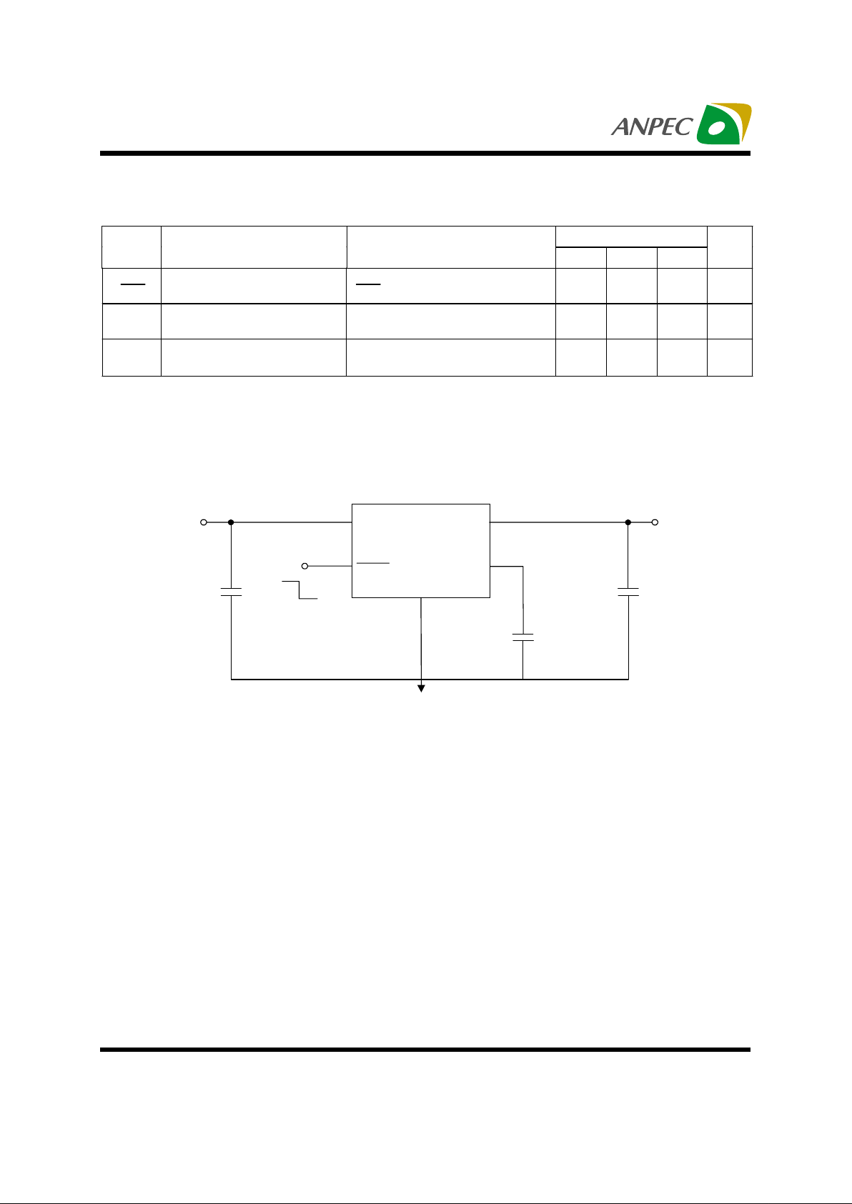
Application Circuit
BP
V
OUT
V
IN
GND
SHDN
VOUT
C
IN
1uF
off
on
APL5301/2
INP UT
2.7V to 6V
0.33uF
C
BP
C
OUT
1uF
Note2 : Dropout voltage definition : VIN-VOUT when VOUT is 2% below the value of VOUT for VIN = VOUT+ 0.5V
Note3 : For 5-pin devices only.
Copyright ANPEC Electronics Corp.
Rev. A.9 - Apr., 2003
APL5301/2
www.anpec.com.tw6
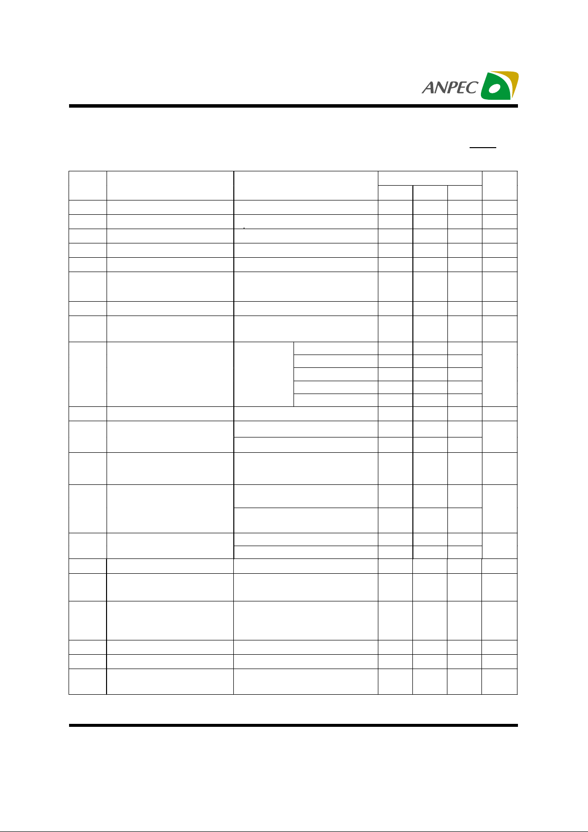
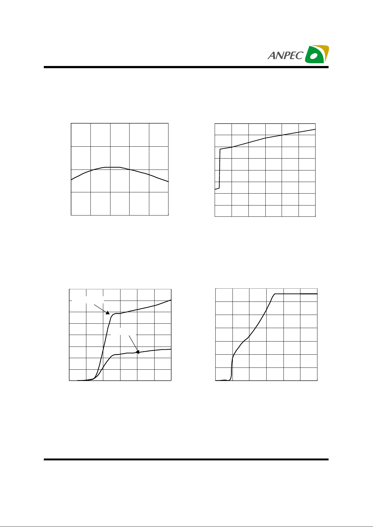
Typical Characteristics
(All Curves are For Fix 3.3V)
0
20
40
60
80
100
120
140
160
0123456
Ground Pin Current vs. Input Voltage
Input Voltage (V)
Ground Pin Current vs. Load Current (uA)
IOUT=50mA
NO LOAD
0
0.5
1
1.5
2
2.5
3
3.5
0123456
Input Voltage vs. Output Voltage
Input Voltage (V)
Output Voltage (V)
0
20
40
60
80
100
120
140
160
0 50 100 150 200 250 300
Ground Pin Current vs. Load Current
Ground Pin Current vs. Load Current (uA)
Load Current (mA)
3.28
3.29
3.3
3.31
3.32
-40 -15 10 35 60 85
Output Voltage vs. Temperature
T emperature (°C )
Output Voltage (V)
 Loading...