


ANPEC APA2020ARI-TY, APA2020ARI-TU, APA2020ARI-TR, APA2020AKI-TY Datasheet
APA2020A
Stereo 2-W Audio Power Amplifier
Features
••
• Low Supply Current , I
••
• Low Shutdown Current , I
= 8mA at Stereo BTL
DD
= 0.5µA
DD
• Depop Circuitry Integrated
• Low Supply Voltage
• Thermal Shutdown Circuitry Integrated
• Output Power at 1% THD+N , V
- 1.8 W/Ch (typ) into a 4 Ω Load
- 1.2 W/Ch (typ) into a 8 Ω Load
DD
=5V
• Bridge-Tied Load (BTL) or Single-Ended
(SE) Modes Operation
• Various 24-Pin Power Packages Available
SOP , TSSOP-P
• High Supply Voltage Ripple Rejection
Applications
• Stereo Audio Power Amplifier for Notebook
Computer
General Description
The APA2020A is a stereo bridge-tied audio power
amplifier in various 24-pin power packages , including SOP , TSSOP-P. When connecting to a 5V voltage supply , the APA2020A is capable of delivering
1.8W/1.2W of continuous RMS power per channel
into 4Ω/8Ω loads with less than 1% THD+N ,
respectively. The APA2020A simplifies design and
frees up board space for other features .
The APA2020A also served well in low-voltage
applications , which provides 800-mW per channel
into 4Ω loads with a 3.3V supply voltage . Both of the
depop circuitry and the thermal shutdown protection
circuitry are integrated in the APA2020A , that reduces
pops and clicks noise during power up and when
using the shutdown or mute modes and protects the
chip from being destroyed by over-temperature
failure.
To simplify the audio system design in notebook
computer applications , the APA2020A combines a
stereo bridge-tied loads (BTL) mode for speaker drive
and a stereo single-end (SE) mode for headphone
drive into a single chip , where both modes are easily
switched by the SE/BTL input control pin signal . For
power sensitive applications , the APA2020A also
features a shutdown function which keeps the supply
current only 0.5 µA (typ) .
Ordering Information
APA2020A
Handling Code
Temp. Range
Package Code
* TSSOP-P is a standard TSSOP package with a thermal pad exposure on the bottom of the package.
ANPEC reserves the right to make changes to improve reliability or manufacturability without notice, and advise
customers to obtain the latest version of relevant information to verify before placing orders.
Copyright ANPEC Electronics Corp.
Rev. A.5 - July., 2002
Package Code
K : SOP R : TSSOP-P *
Temp. Range
I: - 40 to 85 C
Handling Code
TU : Tube TR : Tape & Reel
TY : Tray
°
www.anpec.com.tw1
APA2020A
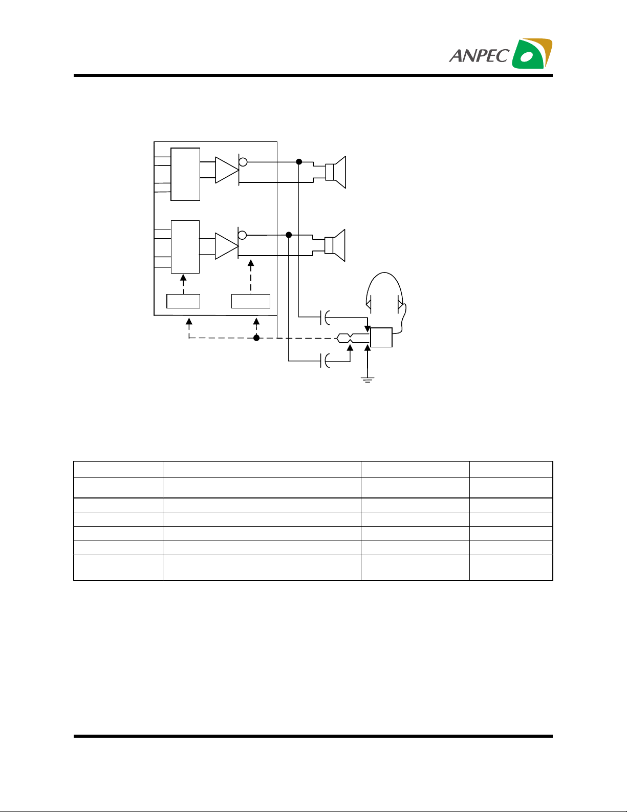
Block Diagram
MUX
MUX
MUX SE/BTL
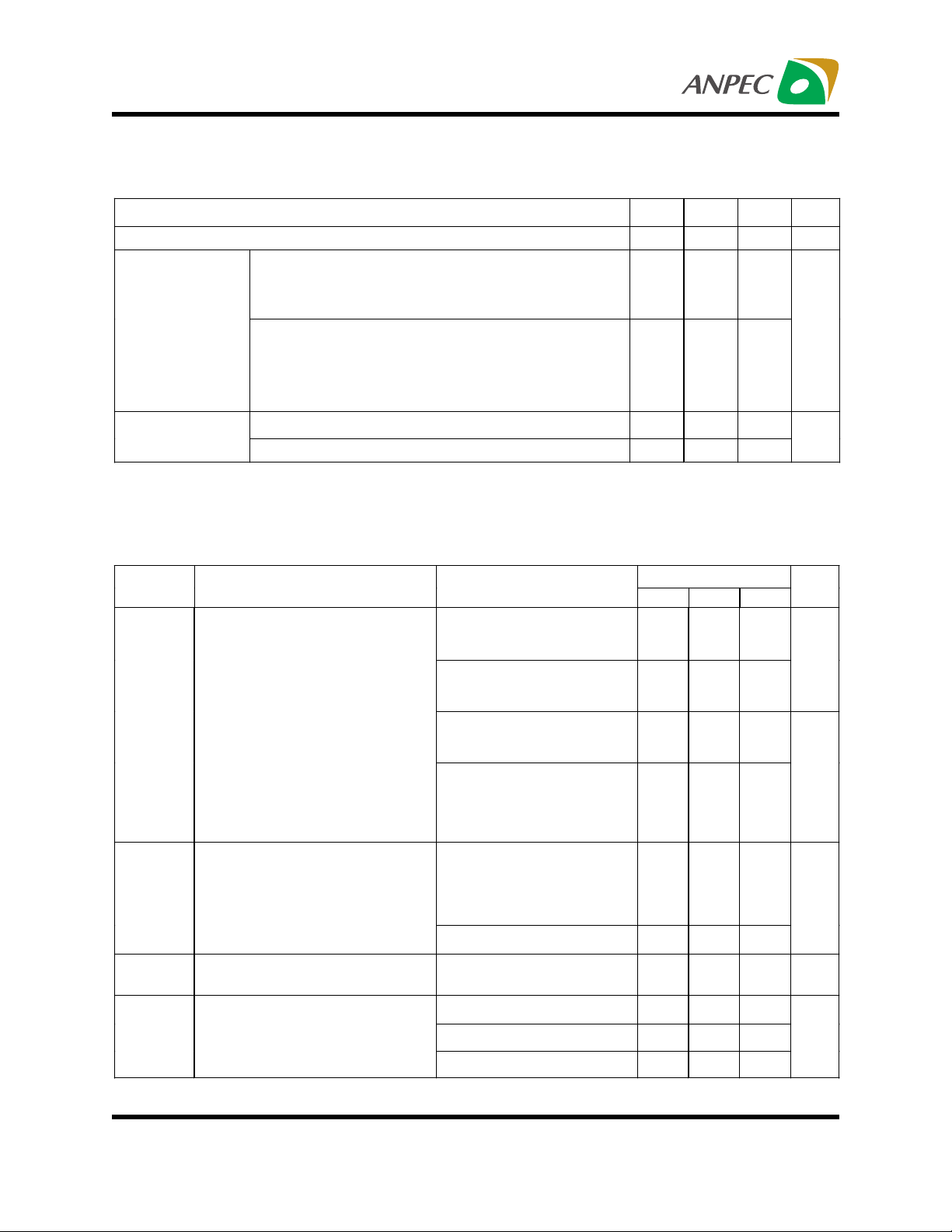
Absolute Maximum Ratings
(Over operating free-air temperature range unless otherwise noted.)
Symbol Parameter Rating Unit
V
CC
T
A
T
J
T
STG
T
S
V
ESD
Note: 1. Human body model : C=100pF , R=1500Ω , 3 positive pulses plus 3 negative pulses
2. Machine model : C=200pF , L=0.5mH , R=0Ω , 3 positive pulses plus 3 negative pulses
Supply Voltage 6 V
Operating Ambient Temperature Range -40 to 85
Maximum Junction Temperature 150
Storage Temperature Range -65 to +150
Soldering Temperature,10 seconds 300
Electrostatic Discharge -3000 to 3000
-200 to 200
*1
*2
C
°
C
°
C
°
C
°
V
Copyright ANPEC Electronics Corp.
Rev. A.5 - July., 2002
www.anpec.com.tw2
APA2020A
Recommended Operating Conditions
Min. Typ. Max. Unit
Supply Voltage, V
DD
355.5V
VDD=5V, 4-Ω stereo BTL drive,
Operating free-air
temperature, T
A
250mW/Ch average power, with proper PCB
design
-20 85
VDD=5V, 3-Ω stereo BTL drive,
2 W/Ch average power, with proper PCB design
-20 85
and 300 CFM
forced-air cooling
Common mode
input voltage, V
VDD=5 V 1.25 4.5
ICM
VDD=3.3V 1.25 2.7
Electrical Characteristics (Cont.)
AC Operating Characteristics , VDD= 5V , TA= 25°C , RL= 4Ω (unless otherwise noted)
Symbol Parameter Test Condition
P(out) Output power (each channel )
see Note 1
THD = 10% , BTL , RL=4
R
THD = 1% , BTL , RL=4
R
THD = 10% , SE , RL=4
R
THD = 1% , SE , R
R
THD = 0.5% , SE , R
THD + N Total harmonic distortion plus
noise
PO = 1.6W , BTL , RL=4
P
= 1W , BTL , RL=8
O
P
= 78mW , SE ,RL=32
O
L
L
L
=4
L
=8
L
=32
L
=8
=8
=8
Ω
Ω
Ω
Ω
Ω
Ω
Ω
Ω
Ω
Ω
Ω
Ω
APA2020A
Min. Typ.Max.
2.3
1.5
1.8
1.2
650
400
500
320
90
300
150
20
C
°
V
Unit
W
mW
m%
B
Maximum output power
OM
bandwidth
Phase margin
Copyright ANPEC Electronics Corp.
Rev. A.5 - July., 2002
= 1V , RL=4
V
1
Ω ,
G = 1
10
G = 10 , THD < 1% >20
RL = 4Ω , BTL
RL = 4Ω , Open Load
R
= 4Ω , SE
L
72
71
52
KHz
°
www.anpec.com.tw3
APA2020A
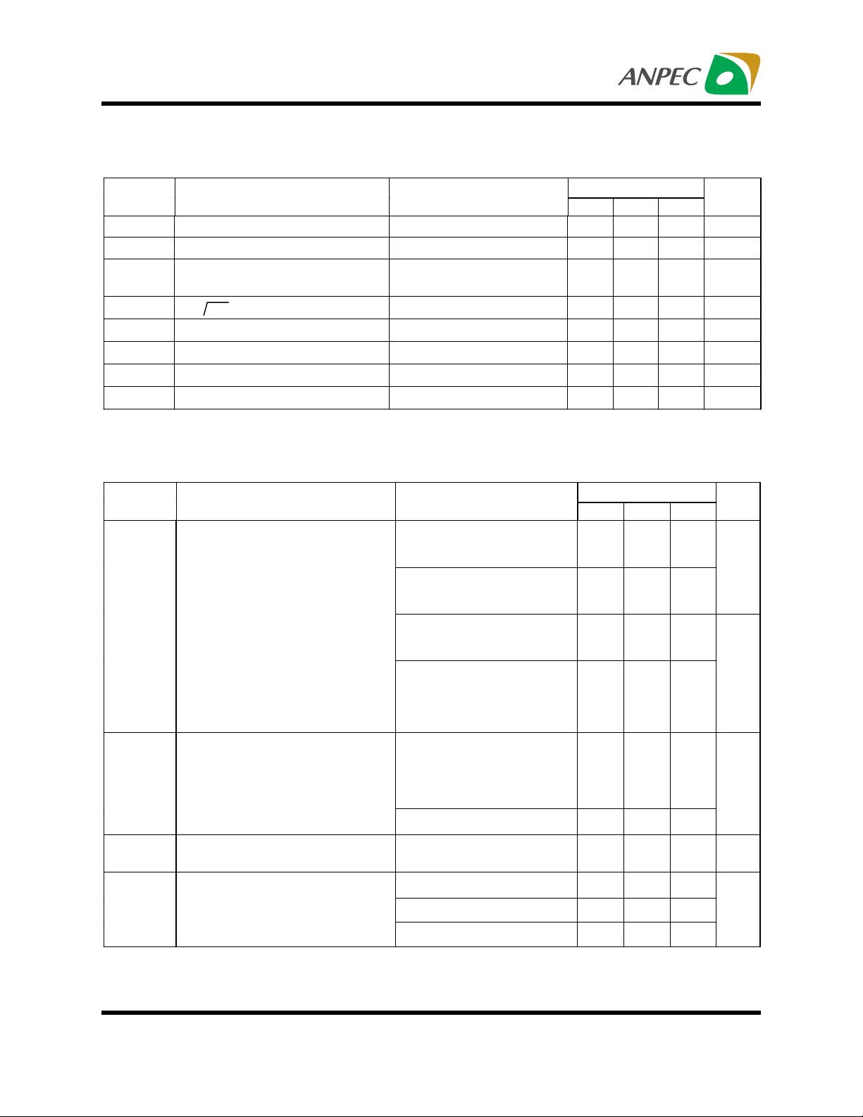
Electrical Characteristics (Cont.)
AC Operating Characteristics , VDD= 5V , TA= 25°C , RL= 4Ω (unless otherwise noted)
Symbol Parameter Test Condition
APA2020A
Min. Typ.Max.
PSRR Power supply ripple rejection f =100 Hz 80 dB
Mute attenuation
Channel-to-channel output
separation
Line HP input separation
BTL attenuation in SE mode
ZI Input impedance
Signal-to-noise ratio Po = 500 mW , BTL
Vn Output noise voltage
85 dB
85 dB
75 dB
80 dB
2
90 dB
80
Notes 1 : Output power is meaured at the output teminals of the IC at 1 KHz.
AC Operating Characteristics , VDD= 3.3V , TA= 25°C , RL= 4Ω (unless otherwise noted)
Symbol Parameter Test Condition
P(out) Output power (each channel )
see Note 2
THD = 10% , BTL , RL=4
R
THD = 1% , BTL , RL=4
R
THD = 10% , SE , RL=4
R
THD = 1% , SE , R
R
THD = 0.5% , SE , R
THD + N Total harmonic distortion plus
noise
PO = 1.6W , BTL , RL=4
P
= 1W , BTL , RL=8
O
P
= 78mW , SE ,RL=32
O
L
=8
L
=8
L
=4
L
=8
L
=32
L
=8
Ω
Ω
Ω
Ω
Ω
Ω
Ω
Ω
Ω
Ω
Ω
Ω
APA2020A
Min. Typ.Max.
1
0.6
0.8
0.5
290
180
230
140
43
270
150
20
Unit
M
V(rms)
µ
Unit
mW
m%
Ω
W
B
Maximum output power
OM
bandwidth
Phase margin
Copyright ANPEC Electronics Corp.
Rev. A.5 - July., 2002
= 1V , RL=4
V
1
Ω ,
G = 1
10
G = 10 , THD < 1% >20 KHz
RL = 4Ω , BTL
RL = 4Ω , Open Load
R
= 4Ω , SE
L
92
70
57
°
www.anpec.com.tw4
APA2020A
)
Electrical Characteristics (Cont.)
AC Operating Characteristics , VDD= 3.3V , TA= 25°C , RL= 4Ω (unless otherwise noted)
Symbol Parameter Test Condition
APA2020A
Min. Typ.Max.
PSRR Power supply ripple rejection f =100 Hz 70 dB
Mute attenuation
Channel-to-channel output
separation
Line HP input separation
BTL attenuation in SE mode
ZI Input impedance
Signal-to-noise ratio Po = 500 mW , BTL
Vn Output noise voltage
f =1 KHz
85 dB
85 dB
75 dB
80 dB
2
90 dB
50
Notes 2 : Output power is meaured at the output teminals of the IC at 1 KHz.
DC Electrical Characteristic , TA=25 °C
APA2020Symbol Parameter Test Conditions
= 5V
V
DD
DD
= 3.3 V
I
DD
Supply Current
Stereo BTL 8 11 mAV
Stereo SE 4 6.5 mA
Stereo BTL 7 9 mA
Typ . Max.
A
Stereo SE 3.5 5.6 mA
V
O (DIFF)
DC Differential Output
=5V, Gain = 2, see Note3 5 25 mV
V
DD
Voltage
I
DD(MUTE
I
SD
Supply Current in Mute Mode V
IDD in Shutdown V
= 5V 8 11 mA
DD
= 5V 0.5 5
DD
Unit
M
V(rms)
µ
Unit
µ
Ω
A
Note 3 : at 3V<VDD<5V , the DC output voltage is approximately V
Copyright ANPEC Electronics Corp.
Rev. A.5 - July., 2002
DD
/ 2.
www.anpec.com.tw5
APA2020A
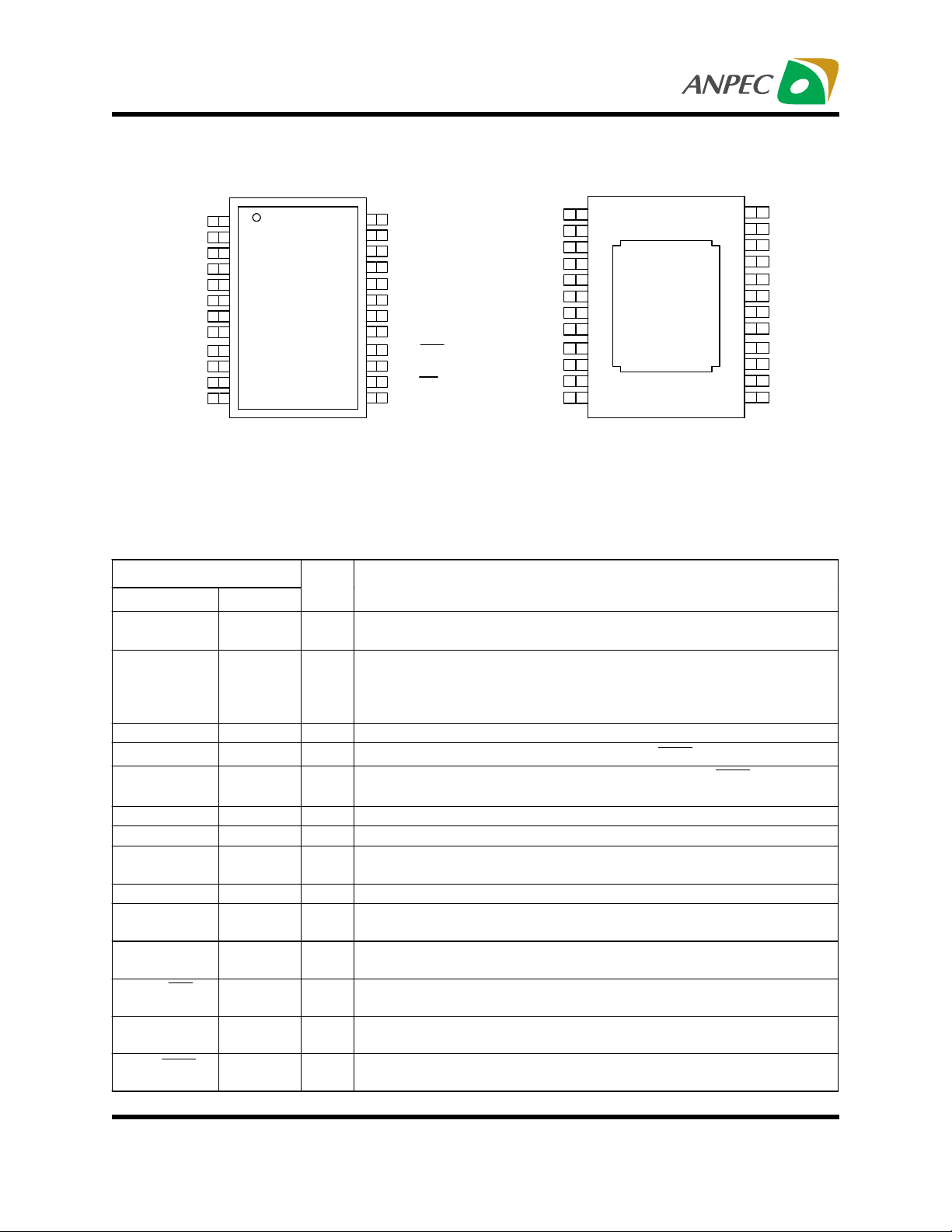
Pin Description
GND/HS
LOUT+
LLINEIN
LHPIN
LBYPASS
LV
SHUTDOWN
MUTE OUT
LOUT-
MUTE IN
GND/HS
T
J
DD
1
2
3
4
5
6
7
8
9
10
11
12
Top View
For SOP and TSSOP-P
Pin
Name No
GND/HS 1,12,
13,24
TJ 2 O
24
23
22
21
20
19
18
17
16
15
14
13
GND/HS
NC
ROUT+
RLINEIN
RHPIN
RBYPASS
RV
DD
NC
HP/LINE
ROUT-
SE/BTL
GND/HS
Thermal
Pad
Bottom View
For TSSOP-P Only
I/O
Description
Ground connection for circuitry, directly connected to thermal pad
(only in TSSOP-P package).
Shutdown mode control signal input, sources a current proportional
to the junction temperature. This pin should be left unconnected
during normal operation. For more information, see the junction
temperature measurement section of this document.
LOUT + 3 O Left channel + output in BTL mode, + output in SE mode.
L LINE IN 4 I
LHP IN
5I
Left channel line input, selected when HP/
pin (16) is held low.
LINE
Left channel headphone input, selected when HP/
LINE
pin (16) is
held high.
LBYPASS 6 Connect to voltage divider for left channel internal mid-supply bias.
LV
DD
7 I Supply voltage input for left channel and for primary bias circuits.
SHUTDOWN 8 I Shutdown mode control signal input, places entire IC in shutdown
mode when held high, I
= 0.5µA.
DD
MUTE OUT 9 O Follows MUTE in pin (11), provides buffered output.
LOUT - 10 O Left channel - output in BTL mode, high-impedance state in SE
mode.
MUTE IN 11 I
Mute control signal input, hold low for normal operation, hold high to
mute.
SE/BTL
14 I Mode control signal input, hold low for BTL mode, hold high for SE
mode.
ROUT- 15 O
Right channel - output in BTL mode, high impedance state in SE
mode.
HP/
LINE
16 I MUX control input, hold high to select headphone inputs (5,20),
hold low to select line inputs (4,21).
Copyright ANPEC Electronics Corp.
Rev. A.5 - July., 2002
www.anpec.com.tw6
APA2020A
Pin Description (Cont.)
Pin
Name No
I/O
Description
NC 17,23 No internal connection.
RV
DD
RBYPASS 19
18 I Supply voltage input for right channel.
Connect to voltage divider for right channel internal mild-supply
bias.
RHP IN 20 I
Right channel headphone input, selected when HP/
held high.
RLINE IN 21 I
Right channel line input, selected when HP/
pin (16) is held
LINE
low.
ROUT+ 22 O Right channel + output in BTL mode, + output in SE mode.
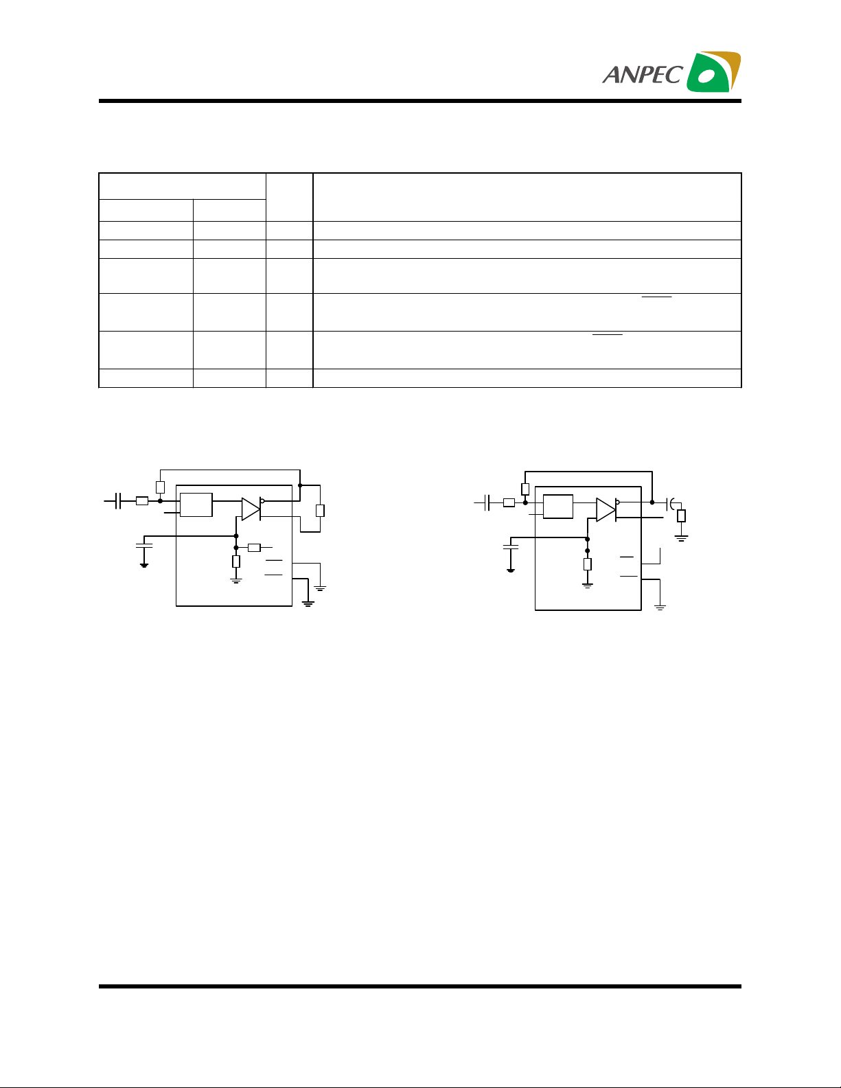
Test Information
R
F
CIR
I
4.7µFC
B
MUX
SE/BTL
HP/LINE
RL=4 Ω , 8Ω or
32 Ω
CIR
4.7µF
R
F
MUX
I
C
B
SE/BTL
HP/LINE
LINE
V
pin (16) is
C
O
RL= 4
or 32
DD
Ω , 8 Ω
Ω
Figure 2. BTL Test Circuit
Copyright ANPEC Electronics Corp.
Rev. A.5 - July., 2002
Figure 3. SE Test Circuit
www.anpec.com.tw7
APA2020A
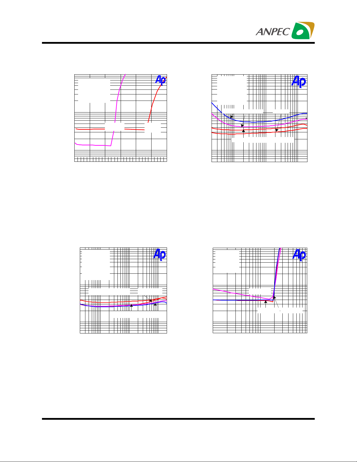
Typical Characteristics
10
VDD=5V
5
f=1 KHz
BTL
2
1
%
0.5
0.2
0.1
0.06
0 3500m 1 1.5 2 2.5
THD+N- Total Harmonic Distortion + Noise
Po - Output Power
RL=8
ΩΩ
Ω
ΩΩ
W
RL=3
ΩΩ
Ω
ΩΩ
Figure 4
10
VDD=5V
5
PO=1.5W
ΩΩ
RL=4
Ω
ΩΩ
BTL
2
AV=20
1
%
0.5
0.2
0.1
0.06
20 20k50 100 200 500 1k 2k 5k
THD+N- Total Harmonic Distortion + Noise
AV=10 AV=2
AV=2
PO=1.8W, RL=3
Hz
f - Frequency
Ω
Figure 5
10
VDD=5V
5
AV=2
ΩΩ
RL=4
Ω
2
1
%
0.5
0.2
0.1
0.06
THD+N- Total Harmonic Distortion + Noise
ΩΩ
BTL
PO=1.8W, RL=3
20 20k50 100 200 500 1k 2k 5k
Ω
PO=0.75W PO=1.5W
Hz
PO=0.25W
f - Frequency
Figure 6
10
VDD=5V
5
RL=3
ΩΩ
Ω
ΩΩ
BTL
2
1
%
0.5
0.2
0.1
0.06
100m 10200m 500m 1 2 5
THD+N- Total Harmonic Distortion + Noise
f=20KHz
f=20Hzf=1KHz
W
Po - Output Power
Figure 7
Copyright ANPEC Electronics Corp.
Rev. A.5 - July., 2002
www.anpec.com.tw8
8
 Loading...