


ANPEC APL1087E-VC-TU, APL1087E-VC-TR, APL1087E-UC-TR, APL1087E-EC-TU, APL1087E-EC-TR Datasheet
...
APL1087E
800mA Low Dropout Fast Response Positive Adjustable Regulator and Fixed
1.8V, 2.5V and 3.3V
Features General Description
••
•
Guaranteed Output Voltage Accuracy within 2%
••
••
•
Fast Transient Response
••
••
•
Guaranteed Dropout Voltage at Multiple Cur-
••
rents
••
•
Load Regulation : 0.6% Typ.
••
••
•
Line Regulation : 0.03% Typ.
••
••
• Low Dropout Voltage : 1.3V Typ. at I
••
••
• Current Limit : 0.8A Min. at T
••
••
• On-Chip Thermal Limiting : 150 °C Typ.
••
••
• Adjustable Output : 1.25~7.15V
••
••
• Standard 3-pin SOT-89, SOT-223,TO-92 and
••
TO-252 Power Packages.
=125°C
J
=500mA
OUT
Applications
••
• Voltage Regulator for CD-ROM Drivers
••
••
• Voltage Regulator for LAN Cards
••
••
• Voltage Regulator for mother Boards
••
••
• Wireless Communication Systems
••
••
• Portable Instrument
••
••
• Portable Consumer Equipment
••
The APL1087E is a low dropout three-terminal adjustable regulators with 0.8A output current capability.
In order to obtain lower dropout voltage and faster
transient response, which is critical for low voltage
applications , the APL1087E has been optimized.
The device is available in an adjustable version and
fixed output voltages of 1.8V, 2.5V and 3.3V, the output available voltage range is from 1.25~7.15V with
an input supply below 9V. Dropout voltage is guaranteed at a maximum of 1.45V at 0.5A.
Current limit is trimmed to ensure specified output
current and controlled short-circuit current. On-chip
thermal limiting provides protection against any combination of overload that would create excessive junction temperatures.
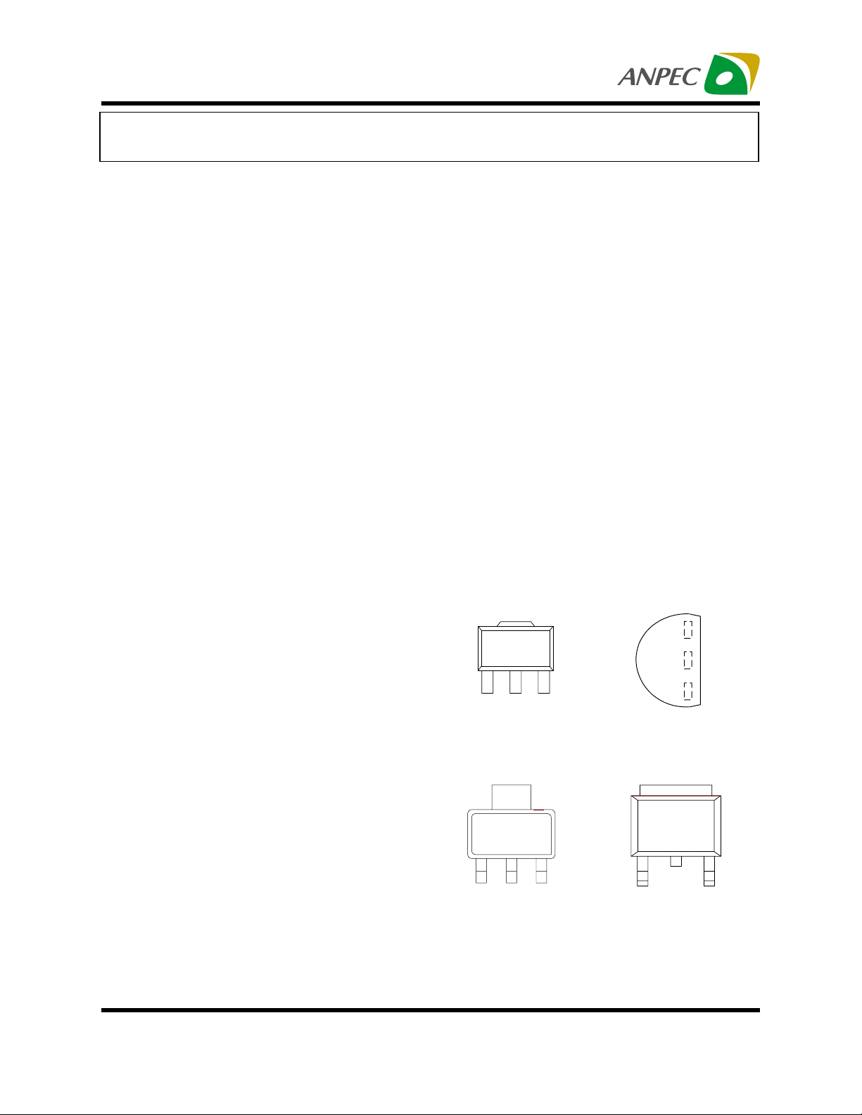
The APL1087E is available in the industry standard
3-pin SOT-89, SOT-223,TO-92 and TO-252 power
packages.
Pin Description
V
IN
GND
213
GND
IN
V
OUT
V
SOT-89 (Front View)
TO-92 (Top View)
V
OUT
••
• Low Voltage Systems
••
123
OUT
V
GND
SOT-223 (Front View)
ANPEC reserves the right to make changes to improve reliability or manufacturability without notice, and advise
customers to obtain the latest version of relevant information to verify before placing orders.
Copyright ANPEC Electronics Corp.
Rev. A.3 - Jun., 2003
IN
V
123
OUT
V
GND
TO-252 (Front View)
www.anpec.com.tw1
IN
V

APL1087E
%
Ordering and Marking Information
APL1087E-
APL1087E U :
APL1087E -18U:
APL1087E -25U:
APL1087E -33U:
APL1087E
XXXXX
18
APL1087E
XXXXX
25
APL1087E
XXXXX
33
APL1087E
XXXXX
XXXXX
XXXXX
XXXXX
XXXXX
Handling Code
Temp. Range
Package Code
Voltage Code
- Date Code
- Date Code
- Date Code
- Date Code
Package Code
D : S OT -8 9 E : T O-9 2
U : T O -2 52 V : S OT -2 23
Temp. Range
C : 0 to 70 C
Handling Code
TU : T u b e T R : T a p e & R e e l
Voltage Code
18 : 1.8 V 25 : 2.5 V 33 : 3 .3V
Blank : Adjustable Version
APL1087E D /V/E :
APL1087E -25D/V/E :
APL1087E -33D/V/E :
°
APL1087E
XXXXX
APL1087E
XXXXX18
APL1087E
XXXXX25
APL1087E
XXXXX33
XXXXX - Date Code
XXXXX - Date CodeAPL1087E -18D/V/E :
XXXXX - Date Code
XXXXX - Date Code
Absolute Maximum Ratings
Symbol Parameter Rating Unit
V
I
T
J
T
STG
T
L
θ
JA
Input Voltage 9 V
Operating Junction Temperature Range
Control Section
Power Transistor
0 to 125
0 to 150
Storage Temperature Range -65 to +150
Lead Temperature (Soldering, 10 second) 260
Thermal Resistance from Junction to Ambient in Free Air
SOT-89
SOT-223
TO-92
TO-252
180
75
180
62.5
°
°
°
C/W
°
C
C
C
Copyright ANPEC Electronics Corp.
Rev. A.3 - Jun., 2003
www.anpec.com.tw2
APL1087E
Electrical Characteristics
Symbol Parameter Test Conditions
REF
Reference
Voltage
V
Output Voltage
APL1087E-18
V
OUT
APL1087E-25
APL1087E-33
Line Regulation
APL1087E
REG
LINE
APL1087E-18
APL1087E-25
APL1087E-33
Load Regulation
APL1087E
REG
LOAD
APL1087E-18
APL1087E-25
APL1087E-33
V
I
LIMIT
I
∆
Dropout Voltage
D
Current Limit
Adjust Pin Current
ADJ
Adjust Pin Current
I
ADJ
Change
Minimum Load
I
O
Current
PSRR Ripple Rejection
Thermal
T
R
Regulation
Temperature
T
S
Stability
Long -Term
L
S
Stability
V
OT
RMS Output
N
Noise
Over Temperature
Point
Quiescent Current
APL1087E-18
APL1087E-25
APL1087E-33
10mA≤ I
T
=0~125°C
J
=0~125°C,
T
J
0≤ I
OUT
T
=0~125°C,
J
0≤ I
OUT
=0~125°C,
T
J
0≤ I
OUT
=0~125°C
T
J
I
10mA, 3.1V≤V
=
OUT
0mA, 3.25V≤V
I
=
OUT
I
0A, 3.95V≤V
=
OUT
0A, 4.75V≤V
I
=
OUT
T
=0~125°C
J
(V
IN –VOUT
V
=3.25V, 0≤ I
IN
=3.95V, 0≤ I
V
IN
=4.75V, 0≤ I
V
IN
I
=0.5A ,T
OUT
(V
IN -VOUT
(V
IN -VOUT
T
0~125°C, 10mA≤ I
=
J
1.45V≤V
T
=0~125°C, V
J
F
RIPPLE
(V
IN -VOUT
T
=25°C, 30ms Pulse
J
=125°C,1000Hrs.
T
J
T
=25°C,10Hz≤F≤10kHz, (% of V
J
=0~125°C,
T
J
V
9V
≤
IN
V
9V
≤
IN
V
9V
≤
IN
0.5A, 3.1V≤V
≤
OUT
0.5A, 3.25V≤V
≤
0.5A, 3.95V≤V
≤
0.5A, 4.75V≤V
≤
IN
IN
≤
IN
≤
IN
)=3V, 0≤ I
J
OUT
0.5A ,(note 1)
≤
OUT
0.5A ,(note 1)
≤
OUT
0.5A ,(note 1)
≤
OUT
=0~125°C
)=5V, TJ=25°C
=3V, I
)
IN -VOUT
=120Hz, V
=3V, TJ=0~125°C
)
=10mA, TJ=0~125°C
OUT
7.55V
≤
=9V, (note 3)
IN
RIPPLE
≤
IN
9V,
≤
IN
9V,
≤
IN
9V,
≤
IN
9V, (note1)
≤
9V, (note1)
≤
9V, (note 1)
9V, (note 1)
0.5A ,(note 1)
≤
0.5A,
≤
OUT
=1V
P-P,
9V,
OUT
APL1087E
Min. Typ. Max.
Unit
1.225 1.250 1.275 V
1.764
2.450
3.235
1.800
2.500
3.300
1.836
2.550
3.365
0.03
1
1
1
0.4 0.6
0.2
6
6
6
V
%
mV
%
1.3 1.45 V
800 mA
60 120
0.2 5
A
µ
A
µ
1.7 mA
60 75 dB
0.01 0.02 %/ W
0.5 %
0.3 %
)
0.003 %
150
5.5
5.5
5.5
10
10
10
°
mA
C
Copyright ANPEC Electronics Corp.
Rev. A.3 - Jun., 2003
www.anpec.com.tw3
APL1087E
Electrical Characteristics (Cont.)
Note 1: See thermal regulation specifications for changes in output voltage due to heating effects. Load line regulations are measured at a constant junction temperature by low duty cycle pulse testing.
Note 2: Dropout voltage is specified over the full output current range of the device. Dropout voltage is defined as the minimum input/
output differential measured at the specified output current. Test points and limits are also shown on the Dropout Voltage curve.
Note 3: Minimum load current is defined as the minimum output current required to maintain regulation.
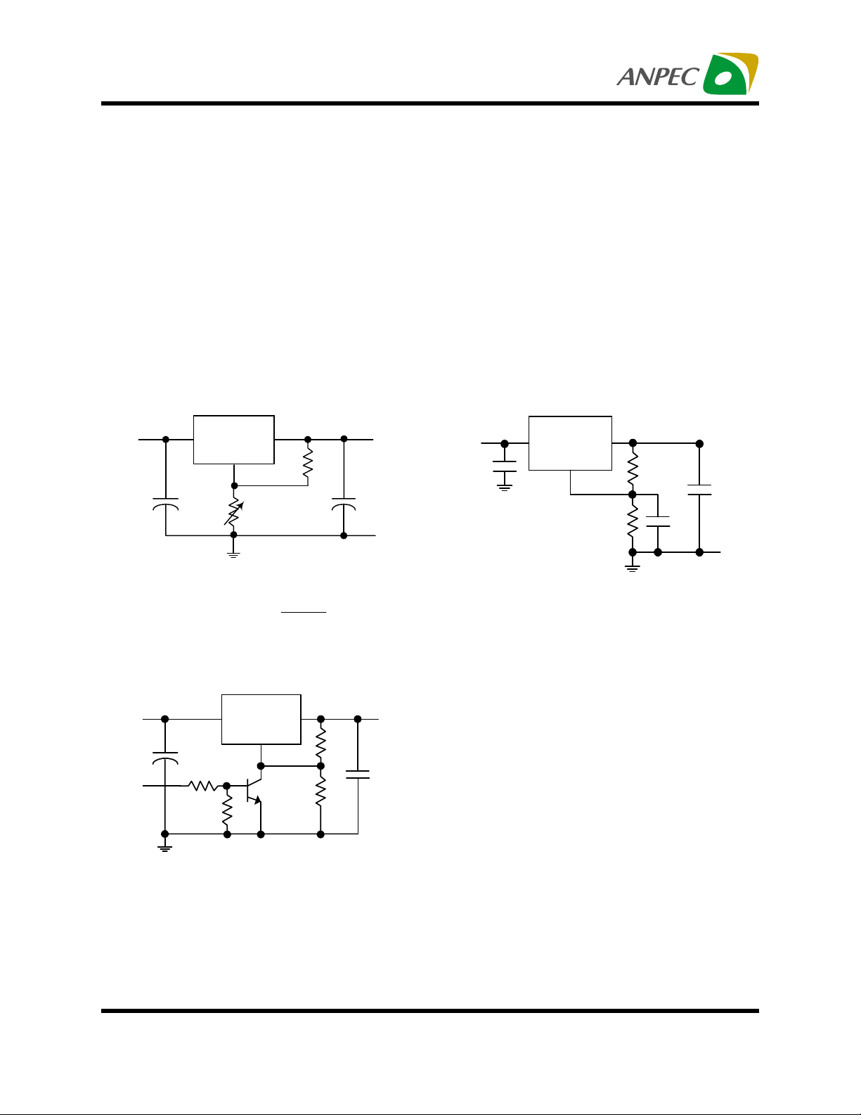
Application Circuits
1.25V to 7.15V Adjustable Regulator Impro ving Ripple Rejection
APL1087E
V
IN
+
10µ
*
C
1
OUTIN
R2
121
R1
Ω
ADJ
F
* Needed if device is far from filter capacitors
OUT
1.250VV
×=
5V Regulator with Shutdown
APL1087E
V
IN
TTL
+
10µ
F
1k
OUTIN
ADJ
1k
+
R1
APL1087E
V
OUT
100µ
+
F
*
C
2
V
10µ
ADJ
OUTIN
R1
IN
+
F
V
OUT
150µF
*
C
3
+
R2
10µ
F
* C3 improves ripple rejection.
R2R1
XC should be approximately
equal to R1 at ripple frequency
5V
Ω
121
1%
+
100µ
365
Ω
F
1%
Copyright ANPEC Electronics Corp.
Rev. A.3 - Jun., 2003
www.anpec.com.tw4
APL1087E
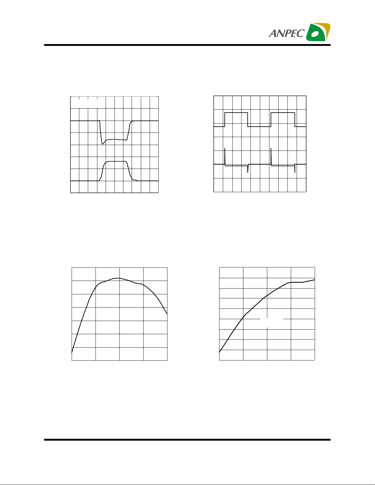
Typical Characteristics
Load Transient Response
10
V
=1.25V
OUT
5
0
-5
-10
-15
-20
-25
Output Voltage Deviation (mV)
-30
0 0.1 0.2 0.3 0.4 0.5 0.6 0.7 0.8 0.9 1
Time (µs)
Adjust Pin Current vs. Temperature
3.5
3
2.5
2
1.5
1
Output Current (A)
0.5
0
-0.5
Line Transient Response
50
40
30
20
10
0
-10
Output Voltage Deviation (mV)
-20
0 0.2 0.4 0.6 0.8 1 1.2 1.4 1.6 1.8 2
Time (µs)
Current Limit vs. Temperature
7
6
5
4
3
Input Voltage (V)
2
1
0
62
61
60
59
58
57
Adjust Pin Current (µA)
56
55
-50 0 50 100 150
Temperature (°C) Temperature(°C)
940
920
900
880
860
840
820
Current Limit (mA)
800
780
760
-50 0 50 100 150
IN=
V
5V
Copyright ANPEC Electronics Corp.
Rev. A.3 - Jun., 2003
www.anpec.com.tw5
 Loading...