


ANPEC APA2121RI-TY, APA2121RI-TU, APA2121RI-TR, APA2120RI-TY, APA2120RI-TR Datasheet
APA2120/2121
Stereo 2-W Audio Power Amplifier (with DC_Volume Control)
Features
••
•
Low operating current with 14mA
••
• Improved depop circuitry to eliminate turn-on
and turn off transients in outputs
• High PSRR
• 32 steps volume adjustable by DC voltage with
hysteresis
• 2W per channel output power into 4Ω load at 5V,
BTL mode
• Two output modes allowable with BTL and SE
modes selected by SE/BTL pin
• Low current consumption in shutdown mode
(50µA)
• Short Circuit Protection
• Power off depop circuit integration
• TSSOP-24 with or without thermal pad package
General Description
APA2120/1 is a monolithic integrated circuit, which
provides precise DC volume control, and a stereo
bridged audio power amplifiers capable of producing
2.7W(2.0W) into 3Ω with less than 10% (1.0%)
THD+N. The attenuator range of the volume control
in APA2120/1 is from 20dB (DC_Vol=0V) to -80dB
(DC_Vol=3.54V) with 32 steps. The advantage of
internal gain setting can be less components and PCB
area. Both of the depop circuitry and the thermal
shutdown protection circuitry are integrated in
APA2120/1, that reduce pops and clicks noise during power up or shutdown mode operation. It also
improves the power off pop noise and protects the
chip from being destroyed by over temperature and
short current failure. To simplify the audio system
Applications
design, APA2120/1 combines a stereo bridge-tied
loads (BTL) mode for speaker drive and a stereo
• NoteBook PC
• LCD Monitor or TV
single-end (SE) mode for headphone drive into a
single chip, where both modes are easily switched
by the SE/BTL input control pin signal. Besides, the
multiple input selection is used for portable audio
system.
Ordering and Marking Information
APA 2120/1
Handling Code
Tem p. Range
Package C ode
AP A2120/1 R :
* TSSOP-P is a standard TSSOP package with a thermal pad exposure on the bottom of the package.
ANPEC reserves the right to make changes to improve reliability or manufacturability without notice, and advise
customers to obtain the latest version of relevant information to verify before placing orders.
Copyright ANPEC Electronics Corp.
Rev. A.1 - Mar., 2003
AP A2120/1
XXXXX
Package C ode
R : TSSOP-P *
Tem p. Range
I : - 4 0 to 8 5 C
Handling Code
T U : T u b e T R : T a pe & R e e l
T Y : T ra y
XXXXX - Date Code
°
www.anpec.com.tw1
APA2120/2121
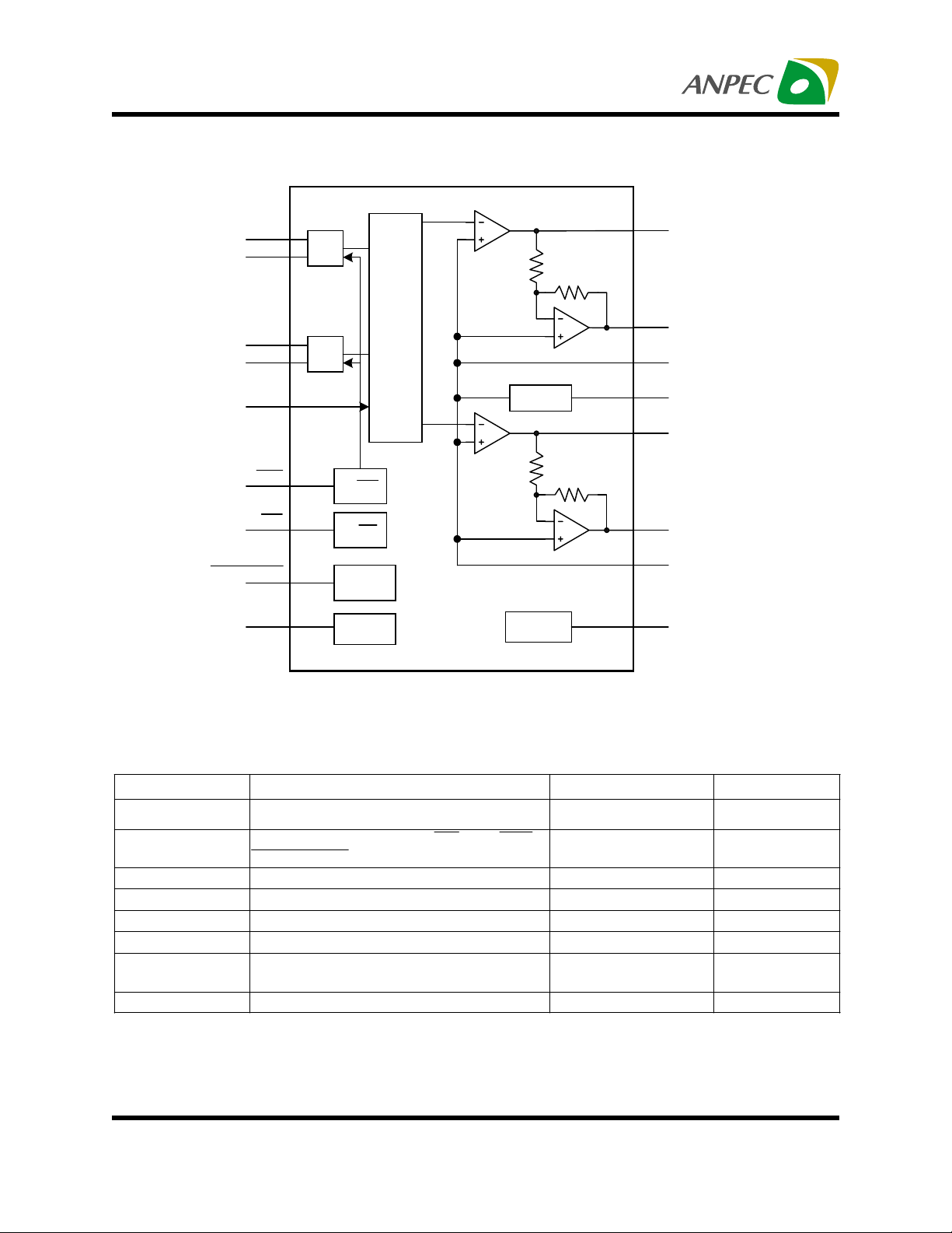
Block Diagram
LLINEIN
LHPIN
RLINEIN
RHPIN
VOLUME
HP/L IN E
SE/BTL
SHUTDOWN
PCBEEP
MUX
MUX
HP /L IN E
SE/BTL
Shutdown
ckt
PC-BEEP
ckt
Volume
Control
BYPASS
Clock Gen
LOUT+
LOUT-
LBYPASS
BYPASS
ROUT+
ROUT-
RBYPASS
CLK
For APA2121
Absolute Maximum Ratings
(Over operating free-air temperature range unless otherwise noted.)
Symbol Parameter Rating Unit
V
DD
V
IN
T
A
T
J
T
STG
T
S
V
ESD
P
D
Note:
1.APA2120/1 integrated internal thermal shutdown protection when junction temperature ramp up to 150°C
2.Human body model: C=100pF, R=1500Ω, 3 positives pulse plus 3 negative pulses
3.Machine model: C=200pF, L=0.5µF, 3 positive pulses plus 3 negative pulses
Copyright ANPEC Electronics Corp.
Rev. A.1 - Mar., 2003
Supply Voltage Range -0.3 to 6 V
Input Voltage Range, SE/BTL, HP/LINE,
SHUTDOWN, PCBEN
-0.3 to V
+0.3 V
DD
Operating Ambient Temperature Range -40 to 85
Maximum Junction Temperature Intermal Limited*
1
Storage Temperature Range -65 to +150
Soldering Temperature,10 seconds 260
2
3
Electrostatic Discharge
-3000 to 3000*
-200 to 200*
Pow e r D issipatio n Inter mal Limited
C
°
C
°
C
°
C
°
V
www.anpec.com.tw2
APA2120/2121
Recommended Operating Conditions
Min. Max. Unit
Supply Voltage, V
DD
High level threshold voltage, V
Low level threshold voltage, V
Common mode input voltage, V
IH
SE/BTL , HP/LINE 4
SHUTDOWN, PCBEN 1.0
SHUTDOWN, PCBEN 2
IL
ICM
SE/BTL , HP/LINE 3
4.5 5.5 V
VDD-1.0 V
Thermal Characteristics
Symbol Parameter Value Unit
R
THJA
Thermal Resistance from Junction to Ambient in Free Air
TSSOP-P* 45 K/W
* 5 in2 printed circuit board with 2oz trace and copper pad through 9 25mil diameter vias.
The thermal pad on the TSSOP_P package with solder on the printed circuit board.
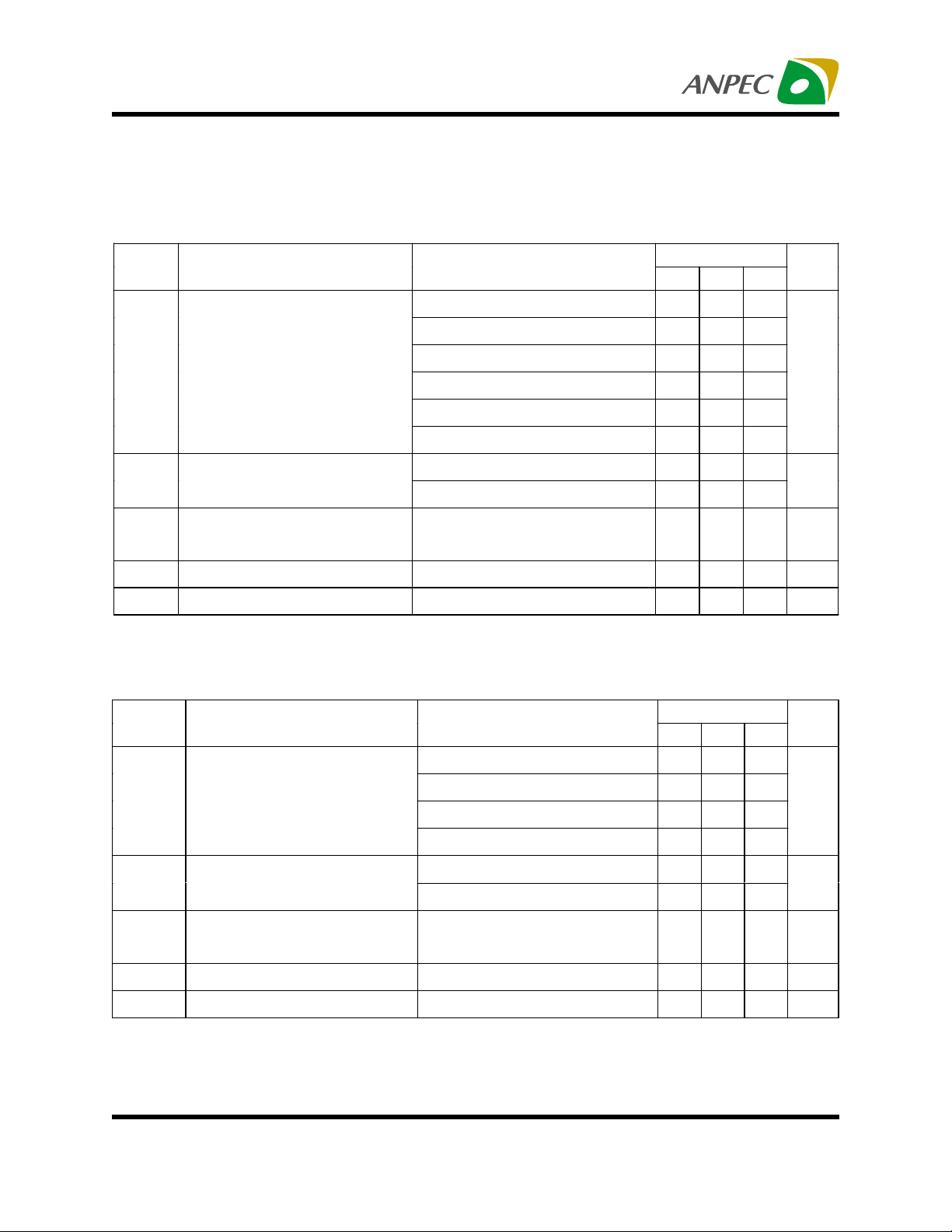
Electrical Characteristics
VDD=5V, -20°C<TA<85°C (unless otherwise noted)
V
V
Symbol Parameter Test Condition
V
DD
Supply Voltage 4.5 5.5 V
SE/BTL=0V
I
DD
I
SD
I
IH
I
IL
V
OS
Copyright ANPEC Electronics Corp.
Rev. A.1 - Mar., 2003
Supply Current
Supply Current in Shutdown
Mode
SE/BTL=5V
SE/BTL=5V
SHUTDOWN=0V
High input Current 900 nA
Low Input Current 900 nA
Output Differential Voltage 5 mV
APA2120/1
Min. Typ. Max.
14 25
8.0 15
50
www.anpec.com.tw3
Unit
mA
A
µ
APA2120/2121
Electrical Characteristics (Cont.)
Operating Characteristics, BTL mode
VDD=5V,TA=25°C,RL=4Ω, Gain=2V/V (unless otherwise noted)
Symbol Parameter Test Condition
THD=10%, RL=3Ω, Fin=1kHz
THD=10%, RL=4Ω, Fin=1kHz
P
O
THD+N
PSRR
Maximum Output Power
Total Harmonic Distortion Plus
Noise
Power Ripple Rejection Ratio
THD=10%, RL=8Ω, Fin=1kHz
THD=1%, RL=3Ω, Fin=1kHz
THD=1%, RL=4Ω, Fin=1kHz
THD=0.5%, R
=8Ω, Fin=1kHz
L
PO=1.5W, RL=4Ω, Fin=1kHz
P
=1W, RL=8Ω, Fin=1kHz
O
V
=0.1Vrms, RL=8Ω, CB=1µF,
IN
Fin=120Hz
APA2120/1
Min. Typ. Max.
2.7
2.3
1.5
2.0
1.9
11.1
0.05
0.07
60 dB
Unit
W
%
Xtalk
S/N
Channel Separation
Signal to Noise Ratio
=1µF, RL=8Ω, Fin=1kHz
C
B
=1.1W, RL=8Ω, A_wieght
P
O
Operating Characteristics, SE mode
VDD=5V,TA=25°C,RL=4Ω, Gain=1V/V (unless otherwise noted)
Symbol Parameter Test Condition
THD=10%, RL=8Ω, Fin=1kHz
THD=10%, RL=32Ω, Fin=1kHz
P
O
THD+N
PSRR
Xtalk
S/N
Maximum Output Power
Total Harmonic Distortion Plus
Noise
Power Ripple Rejection Ratio
Channel Separation
Signal to Noise Ratio
THD=1%, RL=8Ω, Fin=1kHz
THD=1%, R
=32Ω, Fin=1kHz
L
PO=250mW, RL=8Ω, Fin=1kHz
P
=75mW, RL=32Ω, Fin=1kHz
O
=0.1Vrms, RL=8Ω, CB=1µF,
V
IN
Fin=120Hz
C
=1µF, RL=32Ω, Fin=1kHz
B
=75mW, SE, RL=32Ω, A_wieght
P
O
90 dB
95 dB
APA2120/1
Min. Typ. Max.
400
110
320
90
0.08
0.08
48 dB
100
100 dB
Unit
mW
%
dB
Copyright ANPEC Electronics Corp.
Rev. A.1 - Mar., 2003
www.anpec.com.tw4

APA2120/2121
Pin Description
GND
PCBEN
VOLUME
LOUT+
LLINEIN
LHPIN
PVDD
RBYPASS
LOUT-
LBYPASS
BYPASS
GND
1
2
3
4
5
6
7
8
9
10
11
12
APA2120
TOP View
Thermal
Pad
24
23
22
21
20
19
18
17
16
15
14
13
GND
RLINEIN
SHUTDOWN
ROUT+
RHPIN
VDD
PVDD
CLK
ROUTSE/BTL
PC-BEEP
GND
GND
HP/LINE
VOLUME
LOUT+
LLINEIN
LHPIN
PVDD
RBYPASS
LOUT-
LBYPASS
BYPASS
GND
1
2
3
4
5
6
7
8
9
10
11
12
APA2121
TOP View
24
23
22
21
20
19
18
17
16
15
14
13
GND
RLINEIN
SHUTDOWN
ROUT+
RHPIN
VDD
PVDD
CLK
ROUTSE/BTL
PC-BEEP
GND
APA2120/1
Bottom View
Multiple Input Selection PCBEEP Control Input
APA2120 SE/BTL PCBEN
APA2121 HP/LINE -
Copyright ANPEC Electronics Corp.
Rev. A.1 - Mar., 2003
www.anpec.com.tw5
APA2120/2121
Pin Function Description
Pin
Name No
GND
PCBEN 2 I/P BE EP mo de control input, active H, for APA2120 only
HP/LI N E 2 I/P
VOLUME 3 Input signal for internal volume g ain s etting.
LOUT+ 4 O/P
LLIN E IN 5 I/P
LHPIN 6 O/P
PVDD 7,18 Supply voltage only for pow e r a m plifier.
RBYPASS 8 I/P Right channel bypass voltage.
LOUT- 9 O/P
LBYPASS 10 I/P
BYPASS 11 Bias voltage generator
PC_BEEP
SE/BTL 15 I/P
ROUT- 16 O/P
CLK 17 Clock signal generator
VDD 19
RHP IN 20 I/P
ROUT+ 21 O/P
SHUTDOWN 22 I/P
RLIN E IN 23 I/P
1,12,
13,24
Config.
14 I/P
Description
Ground connection, Connected to thermal pad.
Multi-input selection input, headphone mode when held high, line-in
mode when held low for APA2121 only.
Left channel po sitive output in BTL mode and SE mode.
Left channel line input terminal, selected when HP/LINE is held low.
Left channel headphone input terminal, selected when HP/LINE is
held high.
Left channel negative output in BTL mode and high impedance in
SE mode.
Left channel bias voltage generator.
PCBEP signal input
Output mode control input, high for SE output mode and low for
BTL m ode .
Right channel negative output in BTL mode and high impedance in
SE mode.
Supply voltage for internal circuit excepting pow er am p lifier.
Right channel headphone input terminal, selected when HP/LINE is
held high.
Right channel positive output in BTL mode and SE mode.
It will be into shutdown m ode w hen pu ll low.
Right channel line input terminal, selected when HP/LINE is held
low.
Copyright ANPEC Electronics Corp.
Rev. A.1 - Mar., 2003
www.anpec.com.tw6
APA2120/2121
Control Input Table
For APA2120
SE/BTL SHUTDOW N PC-BEEP Operating mode
X L Disable Shutdown mode
L H Disable L ine input, BTL ou t
H H Disable HP input, SE out
X X Enable PCBEEP input, BTL out
For APA2121
SE/BTL HP/LINE SHUTDO WN PC-BEEP Operating mode
X X L Disable Shutdown mode
L L H Disable Line input, BTL out
L H H Disable HP input, BTL out
H L H Disable Line input, SE out
H H H Disable HP input, BTL out
X X X Enable PCBEEP input, BTL out
Copyright ANPEC Electronics Corp.
Rev. A.1 - Mar., 2003
www.anpec.com.tw7
APA2120/2121
Typical Application Circuit
APA2120
L-LIN E
R-LINE
L-HP
R-HP
VDD
0.1
µ
0
Ω
F
100µF
VDD PVDDGND
F
µ
1
F
µ
1
1
F
1
µ
50k
LLINEIN
LHPIN
F
µ
RLINEIN
RHPIN
MUX
MUX
Volume
Control
VDD
BYPASS
VOLUME
Ω
LOUT+
LOUT-
LBYPASS
BYPASS
ROUT+
4
Ω
2.2µF
220
220
F
µ
µ
SE/BTL
F
1k
Ω
Control
Ring
Pin
Sleeve
Tip
Headphone Jack
1k
Ω
VDD
4
100k
SE/BTL
Ω
SE/BTL
ROUT-
Ω
Shutdown
SHUTDOWN
Signal
0.47µF
BEEP
Signal
PCBEN
PCBEEP
PCBEN
Signal
Copyright ANPEC Electronics Corp.
Rev. A.1 - Mar., 2003
Shutdown
ckt
PC-BEEP
ckt
Clock Gen
RBYPASS
CLK
47nF
www.anpec.com.tw8
APA2120/2121
Typical Application Circuit
APA2121
VDD PVDDGND
µF
L-LINE
R-LINE
L-HP
R-HP
1
1
µ
F
1µF
1
µ
F
50k
LLINEIN
LHPIN
RLINEIN
RHPIN
MUX
MUX
Volume
Control
VDD
VOLUME
Ω
VDD
0
Ω
100µF0.1µF
BYPASS
LOUT+
LOUT-
LBYPASS
BYPASS
ROUT+
Ω
4
2.2µF
220
µ
F
SE/BTL
Ω
1k
Control
Ring
Pin
Sleeve
Tip
Headphone Jack
HP /LINE
Signal
Shutdown
Signal
BEEP
Signal
100k
VDD
Ω
SHUTDOWN
0.47µF
HP /LINE
SE/BTL
PCBEEP
HP/LINE
SE/BTL
Shutdown
ckt
PC-BEEP
ckt
Clock Gen
ROUT-
RBYPASS
CLK
47nF
4
Ω
220µF
Ω
1k
Copyright ANPEC Electronics Corp.
Rev. A.1 - Mar., 2003
www.anpec.com.tw9
 Loading...