

APL5308/9
Low IQ, Low Dropout 300mA Fixed Voltage Regulator
Features
• Low Quiescent Current : 60µA (No load)
• Low Dropout Voltage : 400mV (@300mA)
• Fixed Output Voltage : 1.5V ~ 4.5V by Step 0.1V
Increment
• Stable with Aluminum, Tantalum, or Ceramic
Capacitors
• No Protection Diodes Needed
• Built-in Thermal Protection
• Built-in Current-Limit Protection
• Controlled Short Circuit Current : 50mA
• Fast Transient Response
• Short Setting Time
• SOT-23-3, SOT-23-5, and SOT-89 Packages
• Lead Free and Green Devices Available
(RoHS Compliant)
Applications
• 5V to 3.3~4.5V Linear Regulators
• 3.3V to 1.5~2.5V Linear Regulators
• CD-ROM, CD-R/W, and DVD Player
• Networking System, LAN Card, ADSL/Cable
• Modem, Cable Set-Top Box
• PC Peripherals
General Description
The APL5308/9 series are micropower, low dropout linear regulators, which operate from 2.7V to 6V input voltage and deliver up to 300mA. Typic al dropout voltage
is only 400mV at 300mA loading. Designed for use in
battery-powered sys tem, the low 60µA quiescent current makes it an ideal choice. Design with an internal Pchannel MOSFET pass transistor, the APL5308/9 maintain
a low supply current, independent of the load current and
dropout voltage. Other features include thermal-shutdown protection current limit protec tion to ensure
specified output current and c ontrolled short-circuit
current. The APL5308/9 regulators come in a miniature SOT-23-3, SOT-23-5, and SOT-89 packages.
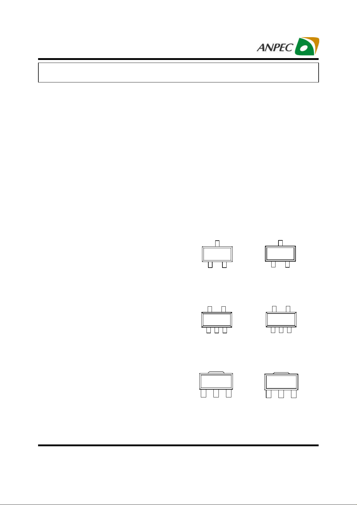
Pin Configuration
VIN
3
1 2
VOUT
GND
SOT-23-3 (Top View)
APL5308
NCNC
45
1 2 3
GND
3
1 2
VOUT VIN
SOT-23-3 (Top View)
APL5309
VOUT NC
45
1 2 3
VIN
GND
VINGND VOUT
SOT-23-5 (Top View)
APL5308
TAB is VIN
1 2 3
GND VIN VOUT
SOT-89 (Top View)
APL5308
ANPEC reserves the right to make changes to improve reliability or manufacturability without notice, and advise
customers to obtain the latest version of relevant information to verify before placing orders.
Copyright ANPEC Electronics Corp.
Rev. A.10 - Dec., 2008
SOT-23-5 (Top View)
APL5309
1 2 3
SOT-89 (Top View)
APL5309
NC
TAB is GND
GND VINVOUT
www.anpec.com.tw1
APL5308/9
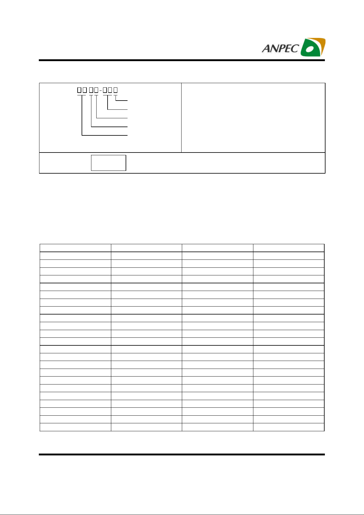
Ordering and Marking Information
APL5308/9
Assembly Material
Handling Code
Temperature Range
Package Code
Voltage Code
APL5308/9 15 D :
Note: ANPEC lead-free products contain molding compounds/die attach materials and 100% matte tin plate termination finish; which
are fully compliant with RoHS. ANPEC lead-free products meet or exceed the lead-free requirements of IPC/JEDEC J-STD-020C for
MSL classification at lead-free peak reflow temperature. ANPEC defines “Green” to mean lead-free (RoHS compliant) and halogen
free (Br or Cl does not exceed 900ppm by weight in homogeneous material and total of Br and Cl does not exceed 1500ppm by
weight).
APL5308/9
XXXXX 15
Package Code
A : SOT-23-3 B : SOT-23-5 D : SOT-89
Operating Ambient Temperature Range
I : -40 to 85 oC C : 0 to 70 oC
Handling Code
TR : Tape & Reel
Voltage Code :
15 : 1.5V ~ 45 : 4.5V
Assembly Material
G : Halogen and Lead Free Device
XXXXX - Date Code ; 15 - 1.5V
Marking Information
SOT-23-3 and SOT-23-5 packages
Product Name Marking Product Name Marking
APL5308-15A/B 389X APL5309-15A/B 399X
APL5308-16A/B 38AX APL5309-16A/B 39AX
APL5308-17A/B 38BX APL5309-17A/B 39BX
APL5308-18A/B 38CX APL5309-18A/B 39CX
APL5308-19A/B 38DX APL5309-19A/B 39DX
APL5308-20A/B 38EX APL5309-20A/B 39EX
APL5308-21A/B 38FX APL5309-21A/B 39FX
APL5308-22A/B 38GX APL5309-22A/B 39GX
APL5308-23A/B 38HX APL5309-23A/B 39HX
APL5308-24A/B 38IX APL5309-24A/B 39IX
APL5308-25A/B 38JX APL5309-25A/B 39JX
APL5308-26A/B 38KX APL5309-26A/B 39KX
APL5308-27A/B 38LX APL5309-27A/B 39LX
APL5308-28A/B 38MX APL5309-28A/B 39MX
APL5308-29A/B 38NX APL5309-29A/B 39NX
APL5308-30A/B 38OX APL5309-30A/B 39OX
APL5308-31A/B 38PX APL5309-31A/B 39PX
APL5308-32A/B 38QX APL5309-32A/B 39QX
APL5308-33A/B 38RX APL5309-33A/B 39RX
APL5308-34A/B 38SX APL5309-34A/B 39SX
APL5308-35A/B 38TX APL5309-35A/B 39TX
APL5308-43A/B 38UX APL5309-43A/B 39UX
APL5308-45A/B 38VX APL5309-45A/B 39VX
The last character “X” in the marking is for data code.
Copyright ANPEC Electronics Corp.
Rev. A.10 - Dec., 2008
www.anpec.com.tw2
APL5308/9
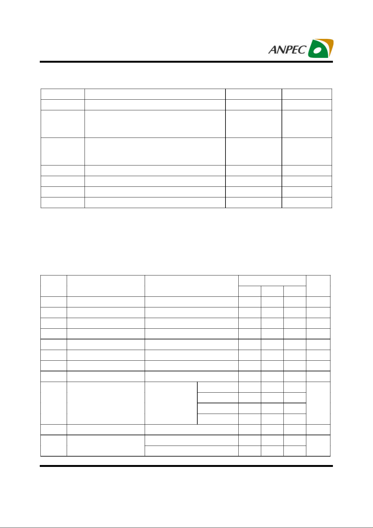
Absolute Maximum Ratings (Note 1, 2)
Symbol Parameter Rating Unit
VIN, V
R
Input Voltage or Out Voltage 6.5 V
OUT
R
TH,JC
TH,JA
Thermal Resistance – Junction to Ambient
SOT-23-3
SOT-23-5
SOT-89
Thermal Resistance – Junction to Case
SOT-23-3
SOT-23-5
SOT-89
260
260
180
130
130
60
°C/W
°C/W
PD Power Dissipation Internally Limited W
T
Junction Temperature 150 °C
JMAX
T
Storage Temperature Range -65 to +150 °C
STG
TL Lead Temperature, 10 Seconds 260 °C
Note 1: Stresses beyond the absolute maximum rating may damage the device and operating in the absolute maximum rating
conditions may affect device reliability.
Note 2: The maximum allowable power dissipation at any TA (ambient temperature) is calculated using: PD (max) = (TJ - TA) / θJA;
TJ = 125oC. Exceeding the maximum allowable power dissipation will result in excessive die temperature.
Electrical Characteristics
Unless otherwise noted these specifications apply over full temperature, C
to TA = 25°C.
Symbol
Parameter Test Conditions
= 1µF, C
IN
= 4.7µF, TA= -40 to 85°C. Typical values refer
OUT
APL5308/9
Unit
Min. Typ. Max.
VIN Input Voltage 2.7 - 6 V
V
Output Voltage V
OUT
I
Circuit Current Limit V
LIMIT
I
Short Current V
SHORT
I
Load Current V
OUT
REG
REG
Line Regulation V
LINE
Load Regulation V
LOAD
Load Transient VIN= V
V
Dropout Voltage
DROP
(Note3)
I
PSRR Ripple Rejection F≤1kHz, 1Vpp at VIN = V
+1.0V< VCC<6.0V, 0mA< I
OUT
= V
+1V - 650 - mA
IN
OUT
= 0V - 50 - mA
OUT
= V
+1V 300 - - mA
IN
OUT
+1V< VCC<6.0V, I
OUT
= V
+1V, 0mA< I
IN
OUT
+1V, I
OUT
OUT
= 1mA - 1 10 mV
OUT
OUT
= 1mA-300mA in 1µs
1.5V≤V
2.0V≤V
=300mA
OUT
2.5V≤V
3V≤V
OUT
< I
V
OUT
MAX
< I
- 10 25 mV
MAX
OUT
-2% V
OUT
V
- 150 250 mV
<2.0V
OUT
<2.5V
OUT
<3V - 0.6 0.7
OUT
≤ 3.5V - 0.4 0.5
OUT
- 1 1.2
- 0.8 0.9
+1.0V 45 55 - dB
No load - 60 100
IQ Quiescent Current
I
= 300mA - 450 500
OUT
Copyright ANPEC Electronics Corp.
Rev. A.10 - Dec., 2008
OUT
www.anpec.com.tw3
+2% V
V
µA
APL5308/9
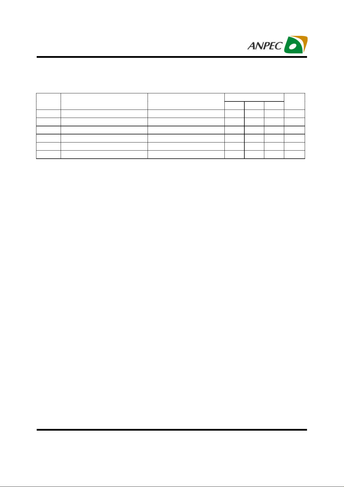
Electrical Characteristics (Cont.)
Unless otherwise noted these specifications apply over full temperature, C
to TA = 25°C.
Symbol
OTS Over Temperature Shutdown
Over Temperature Shutdown Hysteresis Hysteresis
TC Output Voltage Temperature Coefficient
TJ Junction Temperature
C
Output Capacitor
OUT
ESR 0.01 0.1 1 Ohm
Note 3 : Dropout voltage definition : VIN-VOUT when VOUT is 2% below the value of VOUT for VIN = VOUT+1V.
Parameter Test Conditions
-
-
-
= 1µF, C
IN
= 4.7µF, TA= -40 to 85°C. Typical values refer
OUT
APL5308/9
Min. Typ. Max.
150
-
0
30
50
-
2.2
-
-
-
125
-
Unit
°C
°C
ppm/°C
°C
µF
Copyright ANPEC Electronics Corp.
Rev. A.10 - Dec., 2008
www.anpec.com.tw4
APL5308/9
Typical Operating Characteristics
Quiescent Current vs. Input Voltage
450
I
=0mA
OUT
400
350
300
250
200
150
Quiescent Current (µA)
100
50
0
0 1 2 3 4 5 6
Input Voltage (V)
APL5308/9-33
Quiescent Current vs. Output Current
450
400
VIN=5V
0 100 200 300 400 500
Output Current (mA)
Quiescent Current (µA)
350
300
250
200
150
100
50
0
APL5308/9-33
Output Voltage vs. Input Voltage
3.5
I
=0mA
OUT
3
2.5
2
1.5
Output Voltage (V)
1
0.5
0
0 1 2 3 4 5
Input Voltage (V)
Copyright ANPEC Electronics Corp.
Rev. A.10 - Dec., 2008
Output Voltage vs. Temperature
3.31
V
=3.3V
OUT
V
=2.5V
OUT
V
=1.8V
OUT
3.31
3.30
3.30
3.29
Output Voltage (V)
3.29
3.28
3.28
-40 -20 0 20 40 60 80 100 120 140
APL5308/9-33
Temperature (°C )
www.anpec.com.tw5
APL5308/9
Typical Operating Characteristics (Cont.)
Output Voltage vs. Temperature Output Voltage vs. Temperature
2.55
2.54
2.53
2.52
2.51
2.50
2.49
2.48
Output Voltage (V)
2.47
2.46
2.45
-40 -20 0 20 40 60 80 100 120 140
Temperature (°C) Temperature (°C)
APL5308/9-2.5 APL5308/9-1.8
1.84
1.83
1.82
1.81
1.80
1.79
Output Voltage (V)
1.78
1.77
-40 -20 0 20 40 60 80 100 120 140
Dropout Voltage vs. Output Current
700
V
=1.9V
600
500
400
300
200
Dropout Voltage (mV)
100
0
0 50 100 150 200 250 300
Copyright ANPEC Electronics Corp.
Rev. A.10 - Dec., 2008
OUT
V
=2.5V
OUT
V
=3.3V
OUT
Output Current (mA)
PSRR vs. Frequency
+0
APL5308/9-33
VIN=5V
-10
I
=50mA
OUT
-20
-30
-40
-50
PSRR (dB)
- 60
V
=2.8V
OUT
- 70
-80
20
50 100 200 500 1k 2k 5k
10k 20k
50k 100k
200k
Frequency (HZ)
www.anpec.com.tw6

APL5308/9
SOT-25
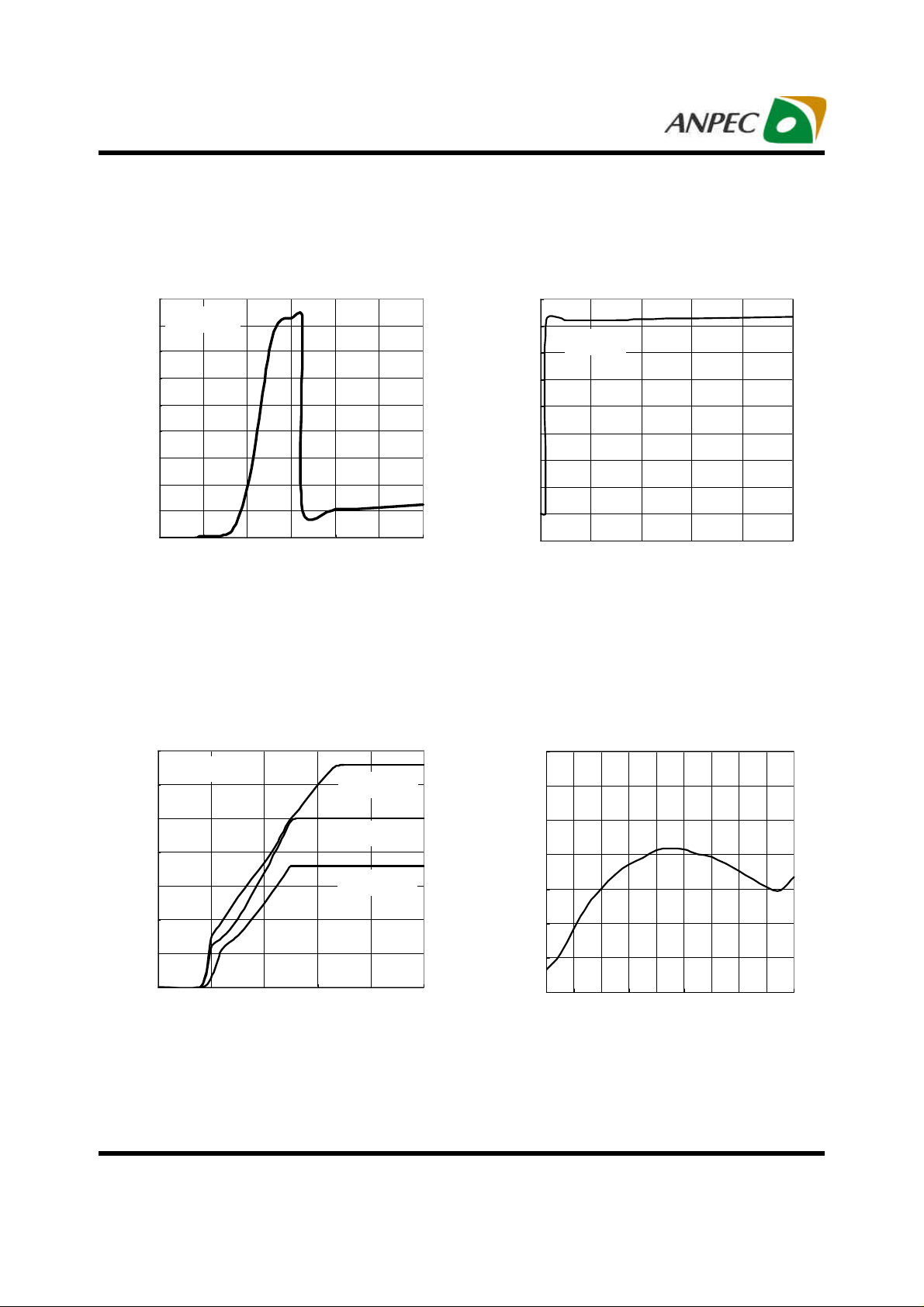
Typical Operating Characteristics (Cont.)
Load-Transient Response
V
OUT
I
=1mA~300mA
Output Voltage (100mV/div)
OUT
Time (100µs/div) Time (200µs/div)
VIN=5V
C
=1µF
OUT
APL5308/9-33
Line-Transient Response
VIN=4.5V~5.5V
C
OUT
I
OUT
Output Voltage (10mV/div)
=1µF
=10mA
APL5308/9-33
V
OUT
Recommended Minimum Footprint
Copyright ANPEC Electronics Corp.
Rev. A.10 - Dec., 2008
Power Dissipation vs. Ambient Temperature
0.8
0.7
0.6
0.5
0.4
0.3
0.2
Power Dissipation (W)
0.1
0
0 25 50 75 100 125
Ambient Temperature (°C)
SOT-89
www.anpec.com.tw7
APL5308/9
Pin Description
PIN
NO. NAME
1 VIN I Supply voltage input.
2 GND
3 V
O Output pin of the regulator.
OUT
I/O FUNCTION
Ground pins of the circuitry, and all ground pins must be soldered
To PCB with proper power dissipation.
Typical Application Circuit
INPUT
2.7V to 6V
CIN
1µF
APL5308/9
GND
VOUTVIN
VOUT
COUT
2.2µF
Copyright ANPEC Electronics Corp.
Rev. A.10 - Dec., 2008
www.anpec.com.tw8

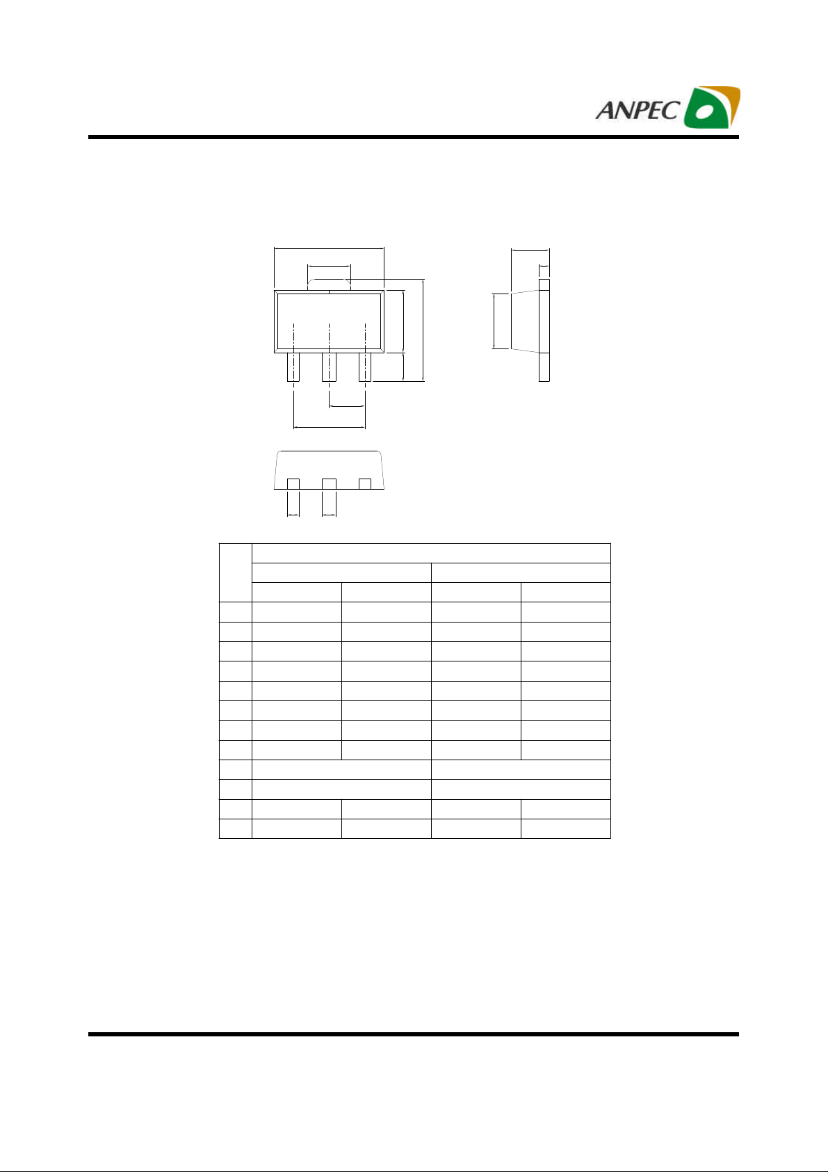
APL5308/9
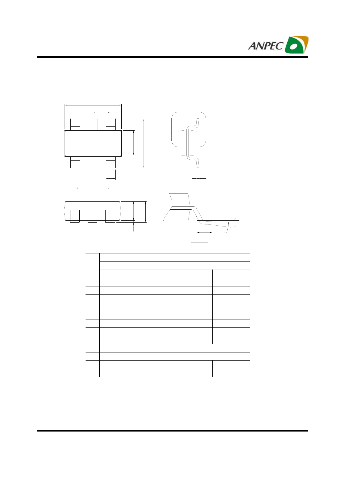
Pack age Information
SOT-23-3
D
e
SEE
VIEW A
E
E1
MIN.
0.000
0.035
0.003
0.106
0.055
0.012
0
c
L
INCHES
0.037 BSC
0.075 BSC
0
MAX.
0.057
0.006
0.051
0.0200.012
0.009
0.122
0.1180.102
0.071
0.024
b
e1
A2
A
A1
VIEW A
S
Y
M
B
O
L
A
A1
A2
b
c
D
E
E1
e
e1
L 0.30
0
Note : Dimension D and E1 do not include mold flash, protrusions or gate
burrs. Mold flash, protrusion or gate burrs shall not exceed 10 mil
per side.
MILLIMETERS
MIN.
0.00
0.90
0.30
0.08
2.70
2.60
1.40
0.95 BSC
1.90 BSC
0
1.45
0.15
1.30
3.10
SOT-23-3
MAX.
0.50
0.22
3.00
1.80
0.60
8
0.25
GAUGE PLANE
SEATING PLANE
8
Copyright ANPEC Electronics Corp.
Rev. A.10 - Dec., 2008
www.anpec.com.tw9
APL5308/9
Pack age Information
SOT-23-5
D
e
b c
e1
SEE
VIEW A
E1
E
A
A2A1
L
VIEW A
0.25
GAUGE PLANE
SEATING PLANE
0
MAX.
1.45
0.15
1.30
0.50
0.22
3.00
1.80
0.60
8
SOT-23-5
MIN.
0.000
0.035
0.003
0.106
0.055
0.012
0
INCHES
MAX.
0.057
0.006
0.051
0.0200.012
0.009
0.122
0.1180.102
0.071
0.037 BSC
0.075 BSC
0.024
8
S
Y
M
B
O
L
A
A1
A2
b
c
D
E
E1
e
e1
L
0
Note : 1. Follow JEDEC TO-178 AA.
2. Dimension D and E1 do not include mold flash, protrusions or gate
burrs. Mold flash, protrusion or gate burrs shall not exceed 10 mil
per side.
MILLIMETERS
MIN.
0.00
0.90
0.30
0.08
2.70
2.60
1.40
0.95 BSC
1.90 BSC
0.30
0
3.10
Copyright ANPEC Electronics Corp.
Rev. A.10 - Dec., 2008
www.anpec.com.tw10
APL5308/9
Pack age Information
SOT-89
B1
S
Y
M
B
O
L
A
B
B1
C
D
D1
E
E1
e
e1
H
L 0.89
MIN. MAX.
1.40
0.44
0.36 0.48
0.35 0.44
4.40 4.60
1.62 1.83
2.29 2.60
2.13
3.94 4.25
D
D1
EL
H
e
e1
B
SOT-89
MILLIMETERS
1.60
0.56
2.29
1.50 BSC 0.059 BSC
3.00 BSC
1.20
E1
INCHES
MIN. MAX.
0.055
0.017
0.014 0.019
0.014 0.017
0.173 0.181
0.064 0.072
0.090 0.102
0.084
0.118 BSC
0.155 0.167
0.035
A
C
0.063
0.022
0.090
0.047
Copyright ANPEC Electronics Corp.
Rev. A.10 - Dec., 2008
Note : Follow JEDEC TO-243 AA.
www.anpec.com.tw11

APL5308/9
Carrier Tape & Reel Dimensions
OD0
B0
P0
P2
P1
A
E1
F
W
Application
SOT-23-3
Application
SOT-23-5
Application
SOT-89
K0
SECTION A-A
T1
B
A
H
A0
SECTION B-B
OD1
B
T
A
d
A H T1 C d D W E1 F
178.0±2.00
50 MIN.
8.4+2.00
-0.00
13.0+0.50
-0.20
1.5 MIN. 20.2 MIN.
8.0±0.30 1.75±0.10 3.5±0.05
P0 P1 P2 D0 D1 T A0 B0 K0
4.0±0.10 4.0±0.10 2.0±0.05
1.5+0.10
-0.00
1.0 MIN.
0.6+0.00
-0.40
3.20±0.20 3.10±0.20 1.50±0.20
A H T1 C d D W E1 F
178.0±2.00
50 MIN.
8.4+2.00
-0.00
13.0+0.50
-0.20
1.5 MIN. 20.2 MIN.
8.0±0.30 1.75±0.10 3.5±0.05
P0 P1 P2 D0 D1 T A0 B0 K0
4.0±0.10 4.0±0.10 2.0±0.05
1.5+0.10
-0.00
1.0 MIN.
0.6+0.00
-0.40
3.20±0.20 3.10±0.20 1.50±0.20
A H T1 C d D W E1 F
178.0±2.00
50 MIN.
12.4+2.00
-0.00
13.0+0.50
-0.20
1.5 MIN. 20.2 MIN.
12.0±0.30 1.75±0.10 5.50±0.05
P0 P1 P2 D0 D1 T A0 B0 K0
4.0±0.10 8.0±0.10 2.0±0.05
1.5+0.10
-0.00
1.5 MIN.
0.6+0.00
-0.40
4.80±0.20 4.50±0.20 1.80±0.20
Copyright ANPEC Electronics Corp.
Rev. A.10 - Dec., 2008
www.anpec.com.tw12

APL5308/9
Devices Per Unit
Package Type Unit Quantity
SOT 23-3
SOT 23-5
SOT-89
Taping Direction Information
SOT-23-3
Tape & Reel 3000
Tape & Reel 3000
Tape & Reel 1000
USER DIRECTION OF FEED
SOT-23-5
SOT-89
USER DIRECTION OF FEED
USER DIRECTION OF FEED
Copyright ANPEC Electronics Corp.
Rev. A.10 - Dec., 2008
www.anpec.com.tw13
APL5308/9
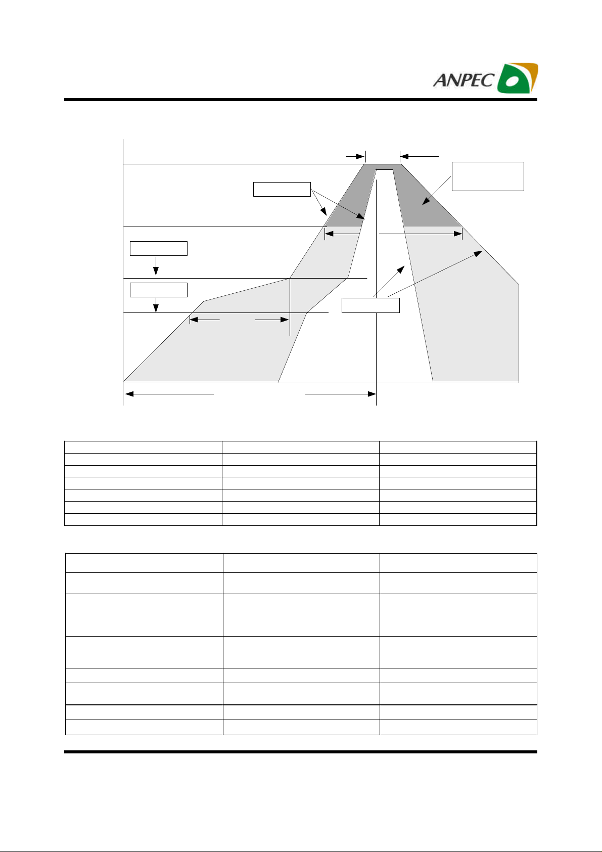
Reflow Condition (IR/Convection or VPR Reflow)
T
P
Ramp-up
T
L
Tsmax
Tsmin
Temperature
ts
Preheat
25
°
t 25 C to Peak
tp
t
L
Ramp-down
Critical Zone
TL to T
Time
Reliability Test Program
Test item Method Description
SOLDERABILITY MIL-STD-883D-2003
HOLT MIL-STD-883D-1005.7
PCT JESD-22-B,A102
TST MIL-STD-883D-1011.9
245°C, 5 sec
1000 Hrs Bias @125°C
168 Hrs, 100%RH, 121°C
-65°C~150°C, 200 Cycles
ESD MIL-STD-883D-3015.7 VHBM > 2KV, VMM > 200V
Latch-Up JESD 78 10ms, 1tr > 100mA
Classification Reflow Profiles
P
Profile Feature Sn-Pb Eutectic Assembly Pb-Free Assembly
Average ramp-up rate
(TL to TP)
Preheat
- Temperature Min (Tsmin)
- Temperature Max (Tsmax)
- Time (min to max) (ts)
Time maintained above:
- Temperature (TL)
- Time (tL)
Peak/Classification Temperature (Tp)
Time within 5°C of actual
Peak Temperature (tp)
Ramp-down Rate
Time 25°C to Peak Temperature
3°C/second max. 3°C/second max.
100°C
150°C
60-120 seconds
183°C
60-150 seconds
150°C
200°C
60-180 seconds
217°C
60-150 seconds
See table 1 See table 2
10-30 seconds 20-40 seconds
6°C/second max. 6°C/second max.
6 minutes max. 8 minutes max.
Notes: All temperatures refer to topside of the package. Measured on the body surface.
Copyright ANPEC Electronics Corp.
Rev. A.10 - Dec., 2008
www.anpec.com.tw14

APL5308/9
Classification Reflow Profiles (Cont.)
Table 1. SnPb Eutectic Process – Package Peak Reflow Temperatures
Package Thickness Volume mm
<350
<2.5 mm
≥2.5 mm 225 +0/-5°C 225 +0/-5°C
Table 2. Pb-free Process – Package Classification Reflow Temperatures
Package Thickness Volume mm3
<350
<1.6 mm
1.6 mm – 2.5 mm
≥2.5 mm 250 +0°C* 245 +0°C* 245 +0°C*
*Tolerance: The device manufacturer/supplier shall assure process compatibility up to and including the stated
classification temperature (this means Peak reflow temperature +0°C. For example 260°C+0°C) at the rated MSL
level.
260 +0°C* 260 +0°C* 260 +0°C*
260 +0°C* 250 +0°C* 245 +0°C*
240 +0/-5°C 225 +0/-5°C
3
Volume mm3
350-2000
Volume mm
≥350
Volume mm3
>2000
3
Customer Service
Anpec Electronics Corp.
Head Office :
No.6, Dusing 1st Road, SBIP,
Hsin-Chu, Taiwan, R.O.C.
Tel : 886-3-5642000
Fax : 886-3-5642050
Taipei Branch :
2F, No. 11, Lane 218, Sec 2 Jhongsing Rd.,
Sindian City, Taipei County 23146, Taiwan, R. O. C.
Tel : 886-2-2910-3838
Fax : 886-2-2917-3838
Copyright ANPEC Electronics Corp.
Rev. A.10 - Dec., 2008
www.anpec.com.tw15

 Loading...