

ANPEC APL5507-B34XC-TR, APL5507-B34OI-TR, APL5507-B34OC-TR, APL5507-B34KI-TR, APL5507-B34KC-TR Datasheet
...
500mA Regulator + Reset IC
Copyright ANPEC Electronics Corp.
Rev. A.4 - Sep., 2002
www.anpec.com.tw1
ANPEC reserves the right to make changes to improve reliability or manufacturability without notice, and advise
customers to obtain the latest version of relevant information to verify before placing orders.
APL5505/6/7
Features General Description
The APL5505/6/7 is micropower, low noise , low dropout regulators with a reset function (regulator input
(APL5505) or specific voltage(APL5506/7) monitoring),
and internal delay circuit, set to detect 3.9V or 4.2V.
Operate from 3V to 6V input voltage and deliver up to
500mA. Typical output noise is just 180uVRMS with an
external 0.01uF bypass capacitor connected in BP
pin and the typical dropout voltage is only 300mV at
500mA loading. Design with an internal P-channel
MOSFET pass transistor, the APL5505/6/7 maintains
a low supply current, independent of the load current
and dropout voltage. Other features include reverse
current protection, thermal-shutdown protection, cur-
rent limit protection to ensure specified output current
and controlled short-circuit current. The APL5505/6/
7 regulators come in miniature SOP-8, TSSOP-8 and
MSOP-8 packages.
Applications
• CD-ROM drive.
••
••
• Low Quiescent Current : 120uA (No load)
••
••
• Low Dropout Voltage : 300mV (VOUT=3.3V@
500mA)
••
••
• Fixed Output Voltage : 1.3V,1.4V,1.5V,1.6V,
1.7V,1.8V,1.9V, 2.0V,2.1V,2.2V,2.3V,2.4V,
2.5V,2.6V,2.7V, 2.8V,2.9V,3.0V,3.1V,3.2V,
3.3V,3.4V.
••
••
• Stable with 4.7uF Output Capacitor
••
••
• Stable with Aluminum , Tantalum or Ceramic
Capacitors .
••
••
• Reverse Current Protection
••
••
• No Protection Diodes Needed
••
••
• Built in Thermal Protection
••
••
• Built in Current Limit Protection
••
••
• Controlled Short Circuit Current : 50mA
••
••
• Fast transient Response
••
••
• Short Setting Time
••
••
• SOP-8,TSSOP-8 and MSOP-8 Packages.
••
••
• Adjustment-free Reset Detection Voltage :
3.9V or 4.2V typ.
• •
• •
• Easy to Set Delay Time from Voltage
Detection to Reset Release.
• •
• •
• Reset and Reset output
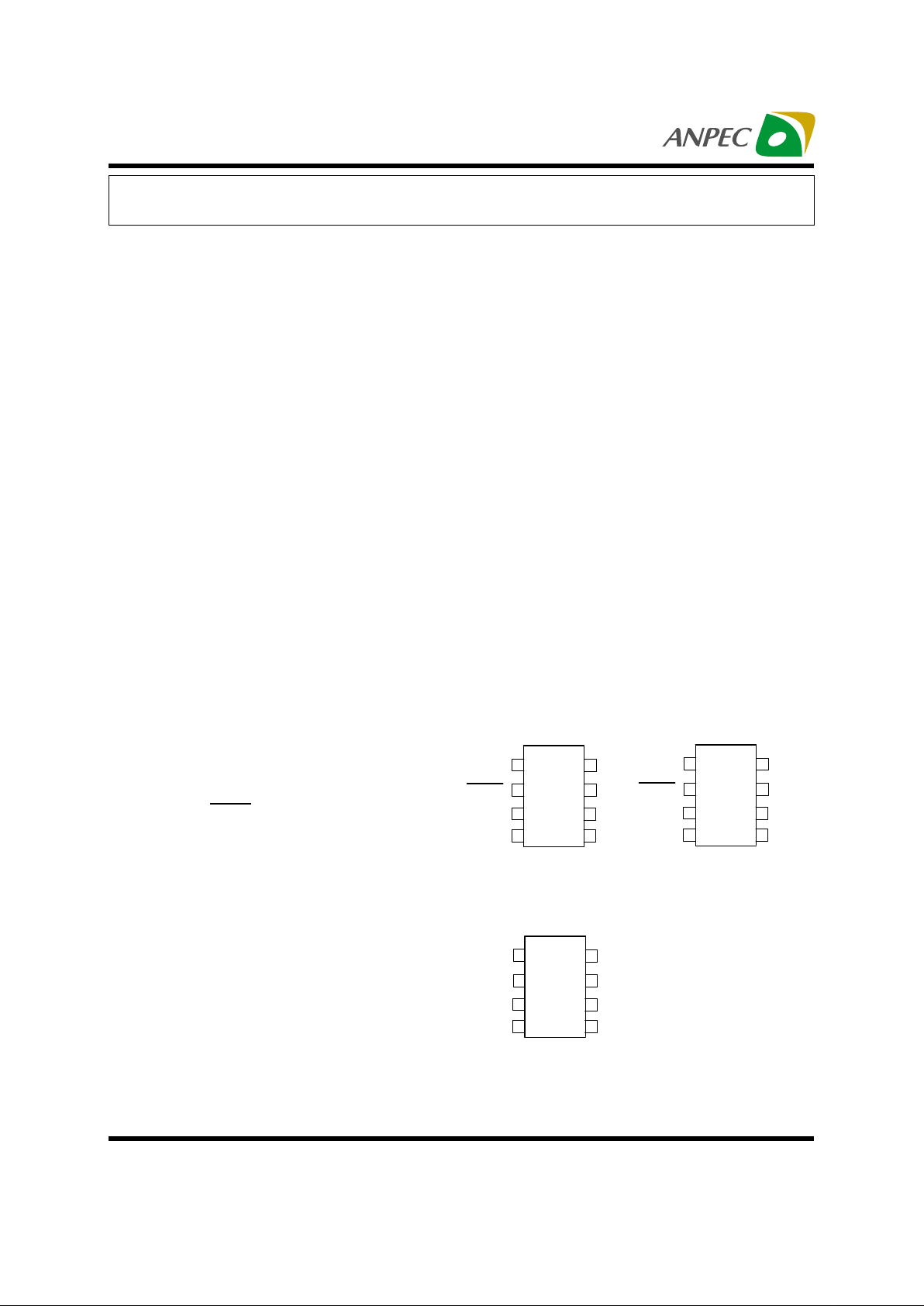
Pin Configuration
RESET
RESET
GND
1
2
3
8
6
475
CONT
V
IN
Bypass
V
OUT
Cd
SOP-8 Top View
APL5505
SOP-8 Top View
APL5506
V
DET
RESET
GND
1
2
3
8
6
475
CONT
V
IN
Bypass
V
OUT
Cd
V
DET
RESET
GND
1
2
3
8
6
475
CONT
V
IN
Bypass
V
OUT
Cd
SOP-8 Top View
APL5507
Copyright ANPEC Electronics Corp.
Rev. A.4 - Sep., 2002
www.anpec.com.tw2
APL5505/6/7
Pin Description
PIN
No. Name
I/O Description
RESET(5505) O Input voltage detection output pin , high = VIN<VS , low = VIN>VS
1
V
DET
(5506/7) I Input pin of voltage detection.
RESET(5507) Input voltage detection output pin , high = VIN<VS , low = VIN>VS
2
RESET(5506)
O
Input voltage detection output pin , low = V
IN
<VS , high = VIN>VS
3 CONT I Output voltage on/off-control pin, low = off , high = on.
4VINO Voltage supply input pin.
5V
OUT
O Regulator output pin.
6 Bypass Bypass signal pin, connect a bypass capacitor to reduce output noise.
7 GND GND pin
8Cd
Delay time capacitor pin, RE SET pin output delay time can be set by
the capacitance connected to the Cd pin. tPLH = 160000.C, tPLH :
transmission delay time (s), C:capacitor value (F)
Symbol Parameter Rating Unit
VIN, V
OUT
Input Voltage or Out Voltage 6 V
CONT Shutdown Control Pin 6 V
Vdet
RESET pin supply voltage 6 V
R
TH,JA
Thermal Resistance – Junction to A mbient 210
°
C/W
P
D
Power Dissip ati on Internally Limit ed W
T
J
Operating Junction Temperature
Control Section 0 to 125
°
C
Power Transistor 0 to 150
T
STG
Storage Temperature R ange -65 to +150
°
C
T
L
Lead Temperature ( Soldering, 10 second) 260
°
C
Absolute Maximum Ratings
Ordering and Marking Information
Package Code
K : SOP-8 O : TSSOP-8
X : MS OP -8
Temp. Range
C : 0 to 7 0 C I : -4 0 to 8 5 C
Handling Code
TR : Tape & Reel
Voltage Code :
13 : 1.3V ~ 34 : 3.4V
Detection Voltage :
A : 3 .9 V B : 4 .2 V
APL5505/6/7 -
Handling Code
Temp. Range
Package Code
Voltage Code
APL5505/6/7X
XXXXX13
APL5505/6/7 :
X - D etec tion V oltage
XXXXX - Date Code , 13 - 1.3V
De tect ion V o lt a g e
°
°
Copyright ANPEC Electronics Corp.
Rev. A.4 - Sep., 2002
www.anpec.com.tw3
APL5505/6/7
Electrical Characteristics
Unless otherwise noted these specifications apply over full temperature , VIN=5V, CIN=4.7uF,COUT=4.7uF,
CONT=V
IN, T
J
=0 to 125°C . Typical values refer to TJ=25°C .
APL5505/6/7
Symbol Parameter Test Conditions
Min. Typ. Max.
Unit
V
IN
Input Voltage 2.7 6 V
V
OUT
Output Voltage V
OUT
+1.0V< VCC<6.0V, 0mA< I
OUT
< I
MAX
V
OUT
-2
%
V
OUT
V
OUT
+2
%
V
I
LIMIT
Circuit Current Limit
V
IN
=5V
700 mA
I
SHORT
Short Current V
OUT
=0V 50 mA
I
OUT
Load Current
500 mA
REG
LINE
Line Regulation V
OUT
+0.5V< VCC<6.0V, 0mA< I
OUT
< I
MAX
16mV
REG
LOAD
Load Regulation VIN =5V, 0mA< I
OUT
< I
MAX
1
6
mV
V
DROP
Dropout Voltage
(Note)
(VOUT(Nominal)=3.0V
Version)
I
OUT
=500mA 300 450 mV
PSRR Ripple Rejection
F≤1kHz, 1Vpp at V
IN
= V
OUT
+1.0V
45 55 dB
I
Q
Quiescent Current No load 120
µ
A
Shutdown Supply
Current
CONT = low
I
OUT
=0, VCC =6.0V
80
µ
A
Noise
100Hz<f<80kHz, typical load,
C
BP
=0.01µF
180
µ
V
Shutdown Recovery
Delay
C
BP
=0.01µF,C
OUT
=1µF, no load
CONT=L!H
400
µ
s
OTS
Over Temperature
150
°
C
Over Temperature
Hysteresis 10
°
C
TC
Output Voltage
Temperature
Coefficient
50 ppm/°C
C
OUT
Output Capacitor 4.7
µ
F
ESR 0.02 0.1 1 Ohm
Shutdown Input
Threshold
V
OUT
+1.0V< VIN <6.0V 1.6 V
I
CONT
Shutdown input Bias
current
V
CONT
=V
IN
0.01 100 nA
Reverse Protection
Threshold
11 50 mV
Note: Dropout voltage definition : VIN-V
OUT
when V
OUT
is 2% below the value of V
OUT
for VIN = V
OUT
+ 0.5V
Copyright ANPEC Electronics Corp.
Rev. A.4 - Sep., 2002
www.anpec.com.tw4
APL5505/6/7
Electrical Characteristics (Cont.)
Unless otherwise noted these specifications apply over full temperature , VIN=5V, CIN=4.7uF,COUT=4.7uF,
CONT=V
IN, T
J
=0 to 125°C . Typical values refer to TJ=25°C .
APL5505/6/7
Symbol Paramete r Test Conditions
Min. Typ. Max.
Unit
RESET/RESET
VIN = H!L (APL5505A)
V
DET
=H!L (APL5506A/5507A)
3.90
VS Detection Voltage
V
IN
= H!L (APL5505B)
V
DET
=H!L(APL5506B/5507B)
4.2
V
µ
VS/
µ6
Vs Temperature
Coefficient
T
J
= -20~+80°C 100 ppm/°C
µ
VS Hysteresis Voltage V
IN
= V
DET
= H!L 100 200 mV
V
OL
Low-level Output
Voltage
V
IN
= V
DET
= 3.9V, RL = 4.7k 30 60 m V
I
OH
Output Leakage
Current
V
IN
= V
DET
= 5V 0.1 uA
IOL1 Output Current1
V
IN
= V
DET
=3.9V, RL = 0
5mA
IOL2 Output Current2
V
IN
= V
DET
= 3.9V, RL = 0
3mA
t
PLH
“H” Transmission D elay
Time
Cd = 0uF 40 90 us
t
PLH1
Reset Delay Time VIN = V
DET
=
3.7V!5V, Cd = 0.1uF 16 ms
t
PHL
“L” Transmission Delay
Time
Cd = 0uF 10 90 us
V
OPL
Threshold Operating
Voltage
V
OL
= 0.4V 0.9 1.1 V
Copyright ANPEC Electronics Corp.
Rev. A.4 - Sep., 2002
www.anpec.com.tw5
APL5505/6/7
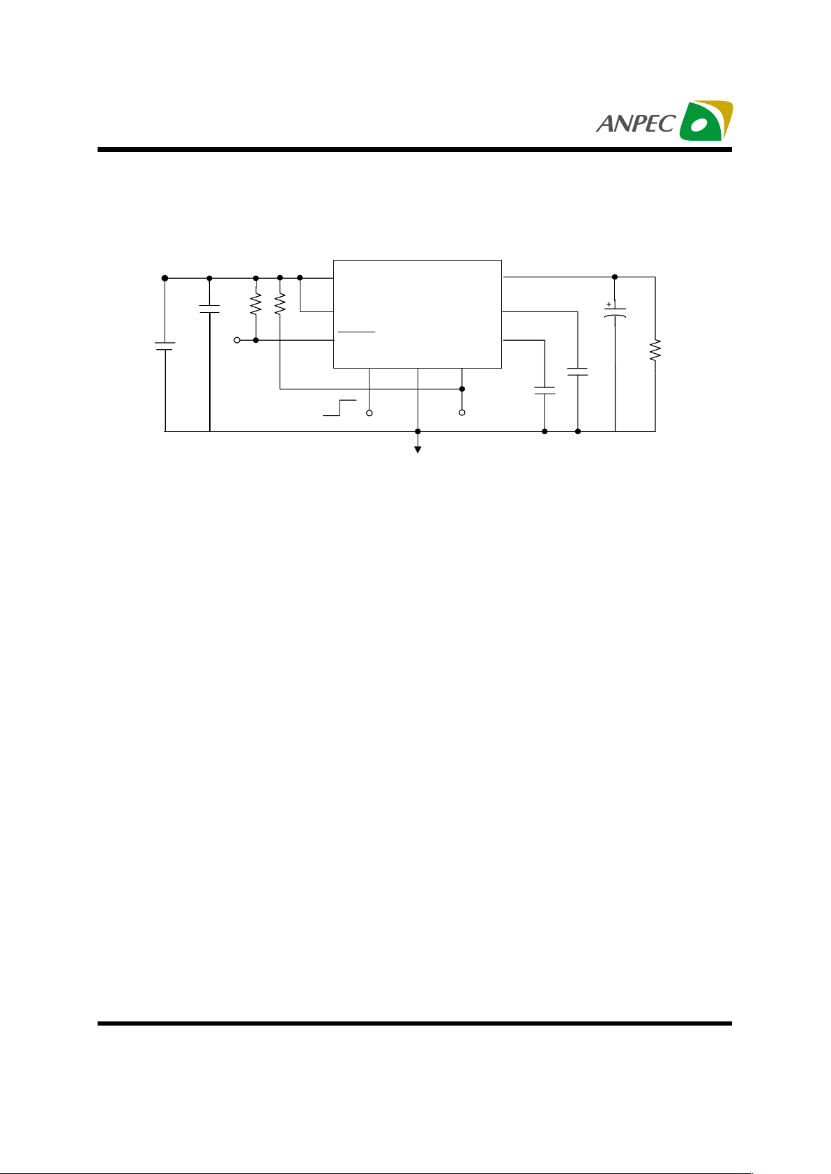
Application Circuit
Cd
V
OUT
V
IN
GND
RESE T(5505/6)
APL5505/6/7
0.01uF
CONT
(5505/7)
RESET
4.7uF
4.7K
Ω
BP
V
DET
(5506/7)
C
OUT
4.7uF
0.1uF

Copyright ANPEC Electronics Corp.
Rev. A.4 - Sep., 2002
www.anpec.com.tw6
APL5505/6/7
0
0.5
1
1.5
2
2.5
3
3.5
0123456
0
20
40
60
80
100
120
140
0123456
0
50
100
150
200
250
0 100 200 300 400 500
500
550
600
650
700
750
44.555.56
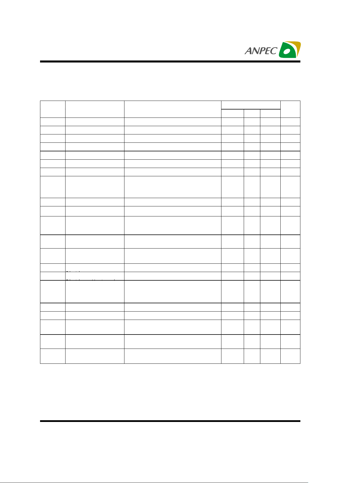
Typical Characteristics
Current Limit vs. Input Voltage
Input Voltage (V)
Current Limit (mA)
Ground Pin Current vs. Load Current
Ground Pin Current (uA)
Load Current (mA)
Input Voltage vs. Output V oltage
Input Voltage (V)
Output Voltage (V)
Ground Pin Current vs. Input Voltage
Ground Pin Current (uA)
Input Voltage (V)

Copyright ANPEC Electronics Corp.
Rev. A.4 - Sep., 2002
www.anpec.com.tw7
APL5505/6/7
-80
+0
-70
-60
-50
-40
-30
-20
-10
20
200
k
50 100 200 500
1k 2k
5k 10k 20k 50k
100k
0
10
20
30
40
50
60
70
80
90
0123456
0
50
100
150
200
250
0 100 200 300 400 500
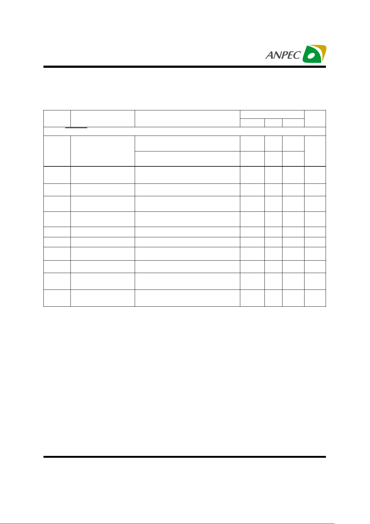
Typical Characteristics
PSRR vs. Frequency
Frequency (HZ)
PSRR (dB)
VIN=4.3V
IOUT =50mA
COUT=1uF
CBP=0.01uF
Reverse Leakage Current vs. Output Voltage
Reverse Leakage Current (uA)
Output Voltage (V)
Dropout Voltage vs. Load Current
Load Current (mA)
Dropout Voltage (mV)
VIN=1V
-1m
1m
-800 u
-600 u
-400 u
-200 u
0
200u
400u
600u
800u
0
100m
20m
40m 60m 80m
Output Noise
Time (s)
VOUT (50uV/div)
VIN=4.3V f=10HZ-80KHZ
IOUT =50mA COUT=1uF
CBP=0.01uF

Copyright ANPEC Electronics Corp.
Rev. A.4 - Sep., 2002
www.anpec.com.tw8
APL5505/6/7
Typical Characteristics
Load-Transient Response
Output Voltage (V)
Time (s)
IOUT=10-500mA
IOUT
Time (s)
COUT=10uF
IOUT=50mA
Line-Transient Response
Output Voltage (V)
VIN
VOUT
VIN=5V
COUT=10uF
VOUT
RESET and RESET Delay Time
Output Voltage (V)
Time (s) Time (s)
Shutdown Recovery Delay
Output Voltage (V)
RESET
CBP=0.01uF
CONT
VOUT
Cd=0.1uF
C
BT=0.01uF
VIN
RESET
0V
0V
5V
5V
0V
5V
0V
0V
4V
3.3V
0A
0.5A
3.3V
2.3V
3.2V
3.3V
4V
5V
0
4m 8m 12m 16m
0.1m0s 0.2m 0.3m 0.4m
0.1m0s 0.2m 0.3m 0.4m 0.5m 0.1m 0.2m 0.3m 0.4m 0.5m0s

Copyright ANPEC Electronics Corp.
Rev. A.4 - Sep., 2002
www.anpec.com.tw9
APL5505/6/7
Typical Characteristics
0.001
0.01
0.1
1
10
0 100 200 300 400 500
Region of Stable ESR vs. Load Current
Load Current (mA)
Stable
Region
VOUT=3.3V
Unstable
Region
Region of Stable ESR

Copyright ANPEC Electronics Corp.
Rev. A.4 - Sep., 2002
www.anpec.com.tw10
APL5505/6/7
Packaging Information
Millimeters Inches
Dim
Min. Max. Min. Max.
A 1.35 1.75 0.053 0.069
A1 0.10 0.25 0.004 0.010
D 4.80 5.00 0.189 0.197
E 3.80 4.00 0.150 0.157
H 5.80 6.20 0.228 0.244
L 0.40 1.27 0.016 0.050
e1 0.33 0.51 0.013 0.020
e2 1.27BSC 0.50BSC
φ
18
°
8
°
HE
e1 e2
0.015X45
D
A
A1
0.004max.
1
L
SOP-8 pin ( Reference JEDEC Registration MS-012)

Copyright ANPEC Electronics Corp.
Rev. A.4 - Sep., 2002
www.anpec.com.tw11
APL5505/6/7
Packaging Information
TSSOP
Millimeters Inches
Dim
Min. Max. Min. Max.
A 1.2 0.047
A1 0.00 0.15 0.000 0.006
A2 0.80 1.05 0.031 0.041
b 0.19 0.30 0.007 0.012
D 2.9 3.1 0.114 0.122
e 0.65 BSC 0.026 BSC
E 6.40 BSC 0.252 BSC
E1 4.30 4.50 0.169 0.177
L 0.45 0.75 0.018 0.030
L1 1.0 REF 0.039REF
R 0.09 0.004
R1 0.09 0.004
S 0.2 0.008
φ
10
°
8
°
0
°
8
°
φ
212
°
REF 12° REF
φ
312
°
REF 12° REF
L
(L1)
(3)
S
(2)
0.25
GAUGE
PLANE
1
b
D
e
2 x E / 2
8
12
e/2
E1 E
7
A1
A2
A

Copyright ANPEC Electronics Corp.
Rev. A.4 - Sep., 2002
www.anpec.com.tw12
APL5505/6/7
e1
E1
E
e1
A1
A2
L2
L1
A3
Millimeters Inches
Dim
Min. Max. Min. Max.
A1 0.06 0.15 0.002 0.006
A2 0.86 TYP 0.34 TYP
A3 0.25 0.4 0.01 0.0126
e 0.65 TYP 0.0256TYP
e1 2.90 3.1 0.114 0.124
E 4.8 5.0 0.189 0.197
E1 2.90 3.1 0.169 0.177
L1 0.25 REF 0.039REF
L2 0.0375 REF 0.953 REF
MSOP
Packaging Information

Copyright ANPEC Electronics Corp.
Rev. A.4 - Sep., 2002
www.anpec.com.tw13
APL5505/6/7
Physical Specifications
Pre-heat temperature
183 C
Peak temperature
Time
°
temperature
Classification Reflow Profiles
Convection or IR/
Convection
VPR
Average ramp-up rate(183°C to Peak) 3°C/second max. 10 °C /second max.
Preheat temperature 125 ± 25°C)
120 seconds max
Temperature m aintained above 183°C
60 – 150 seconds
Time within 5°C of actual peak temperature
10 –20 seconds 60 seconds
Peak temperature range
220 +5/-0°C or 235 +5/-0°C 215-219°C or 235 +5/-0°C
Ramp-down rate
6 °C /second max. 10 °C /second max.
Time 25°C to peak temperature
6 minutes max.
Package Reflow Conditions
pkg. thickness
≥≥≥≥
2.5mm
and all bgas
pkg. thickness < 2.5mm and
pkg. volume
≥≥≥≥
350 mm³
pkg. thickness < 2.5mm and pkg.
volume < 350mm³
Convection 220 +5/-0 °C Convection 235 +5/-0 °C
VPR 215-219 °C VPR 235 +5/-0 °C
IR/Convection 220 +5/-0 °C IR/Convection 235 +5/-0 °C
Terminal Material Solder-Plated Copper (Solder Material : 90/10 or 63/37 SnPb)
Lead Solderability Meets EIA Specification RSI86-91, A NSI/J-STD-002 Category 3.
Reference JEDEC Standard J-STD-020A APRIL 1999
Reflow Condition (IR/Convection or VPR Reflow)

Copyright ANPEC Electronics Corp.
Rev. A.4 - Sep., 2002
www.anpec.com.tw14
APL5505/6/7
R e lia bility t e st p r o g ra m
Test item Method Descrip tion
SOLDERABILITY MIL-STD-883D-2003
245°C , 5 SEC
HO LT MIL-STD-883D-1005.7
1000 Hrs Bias @ 125 °C
PCT JESD-22-B, A102
168 Hrs, 100 % RH , 121°C
TST MIL-STD-883D-1011.9
-65°C ~ 150°C, 200 Cycles
ESD MIL-STD-883D-3015.7 VHB M > 2KV, VMM > 200V
La tc h -Up J E S D 78 1 0m s , Itr > 100mA
Carrier Tape
A
J
B
T2
T1
C
t
Ao
E
W
Po
P
Ko
Bo
D1
D
F
P1

Copyright ANPEC Electronics Corp.
Rev. A.4 - Sep., 2002
www.anpec.com.tw15
APL5505/6/7
Application
A B C J T1 T2 W P E
330 ± 1 62 +1.5
12.75+
0.15
2 ± 0.5 12.4 ± 0.2 2 ± 0.2 12± 0. 3 8± 0.1 1.75±0.1
F D D1 Po P1 Ao Bo Ko t
SOP- 8
5.5± 1 1.55 +0.1 1.55+ 0.25 4.0 ± 0.1 2.0 ± 0.1 6.4 ± 0.1 5.2± 0. 1 2.1± 0.1 0.3±0.013
Application
A B C J T1 T2 W P E
330 ± 1 62 +1.5
12.75+
0.15
2 + 0.5 12.4 ± 0.2 2 ± 0.2 12± 0. 3 8± 0.1 1.75±0.1
F D D1 Po P1 Ao Bo Ko t
TSSOP-8
5.5 ± 0. 1 1.5 + 0.1 1.5 + 0.1 4.0 ± 0.1 2.0 ± 0.1 7.0 ± 0.1 3.6 ± 0.3 1.6 ± 0.1 0.3±0.013
Application Carrier W idth Cover Tape Width Devices Per Reel
SOP- 8
12 9.3 2500
TSSOP- 8
12 9.3 2500
Cover Tape Dimensions
Anpec Electronics Corp.
Head Office :
5F, No. 2 Li-Hsin Road, SBIP,
Hsin-Chu, T aiwan, R.O.C.
T el : 886-3-5642000
Fax : 886-3-5642050
Taipei Branch :
7F, No. 137, Lane 235, Pac Chiao Rd.,
Hsin Tien City, Taipei Hsien, Taiwan, R. O. C.
T el : 886-2-89191368
Fax : 886-2-89191369
Customer Service
Reel Dimensions
 Loading...