


ANPEC APL158125U5C-TU, APL158125U5C-TR, APL158125G5C-TU, APL158125G5C-TR, APL158125F5C-TU Datasheet
...
DUAL INPUT LOW DROPOUT REGULATOR
Copyright ANPEC Electronics Corp.
Rev. A.8 - Oct., 2003
APL1581
www.anpec.com.tw1
ANPEC reserves the right to make changes to improve reliability or manufacturability without notice, and advise
customers to obtain the latest version of relevant information to verify before placing orders.
Features General Description
The APL1581 series of high performance positive voltage regulators are designed for use in applications
requiring very low dropout voltage at 5Amp.
The APL1581 can provide a output voltage at the range
of 1.25V to 2.55V , where both 5V and 3.3V voltage
supplies are available.
The superior dropout characteristics result in reduced
heat dissipation compared to regular LDOs. The
APL1581 also provides excellent regulation over line
, load , and temperature variations.
Current limit is trimmed to ensure specified output
current and controlled short-circuit current. On-chip
thermal limiting provides protection against any combination of overload that would create excessive junction temperature.
The APL1581 is available in both the through-hole
and surface mount versions of the industry standard
5-Pin TO-220 and TO-263, TO-252 power packages.Applications
• Microprocessor Supplies
•! Chip Set Supplies
• VGA Card Power
• LCD Monitor Power
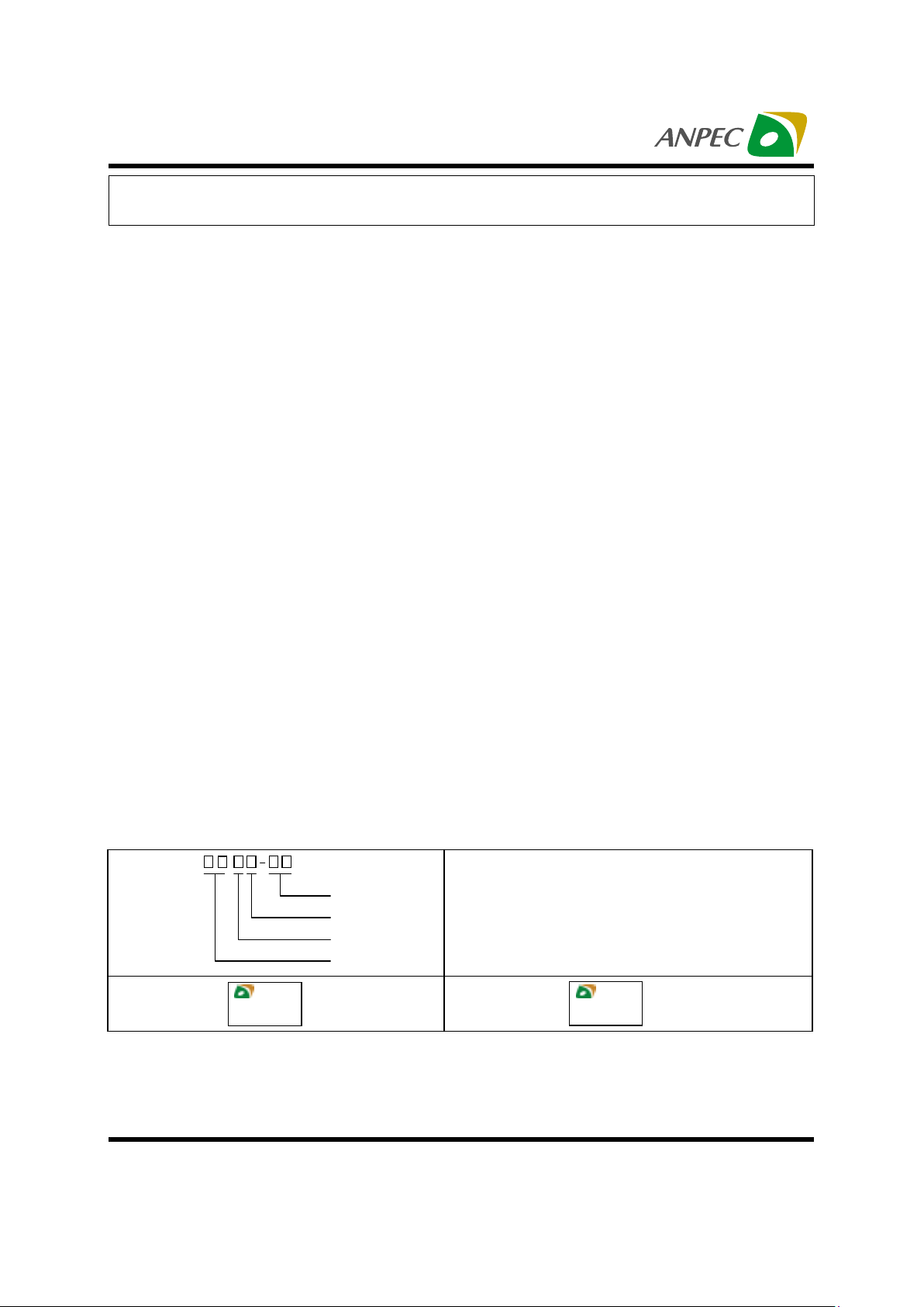
Ordering and Marking Information
••
••
•
Adjustable or Fixed Output
••
••
•
520mV typ. Dropout at 5A in dual power
voltage mode
••
••
•
Remote Sense Pin Available
••
••
•
2% Accuracy Over Temperature Range
••
••
•
Build-in Over Temperature Protection
••
••
• Build-in Current Limit
••
••
• 5 Pin TO-220 and TO-263, TO-252
Packages
••
••
• No Supply Sequencing Problems in Dual
Supply Mode
Package C ode
F5 : T O -2 20 -5 G 5 : T O -2 63 -5 U 5 :T O -2 52 -5
Temp. Range
C : 0 to 7 0 C
Handling Code
TU : T u be TR : Ta p e & Ree l
Voltage Code :
15 : 1.5 V 18 : 1.8 V
25 : 2.5V
APL1581
Handling Code
Temp. Range
Package C ode
Voltage Code
APL1 581F/G/U :
APL1 581
XXXXX
XXXXX - Date Code
APL1 581-15 :
APL1581
XXXXX
XXXXX - Date Code
15
o
Copyright ANPEC Electronics Corp.
Rev. A.8- Oct., 2003
APL1581
www.anpec.com.tw2
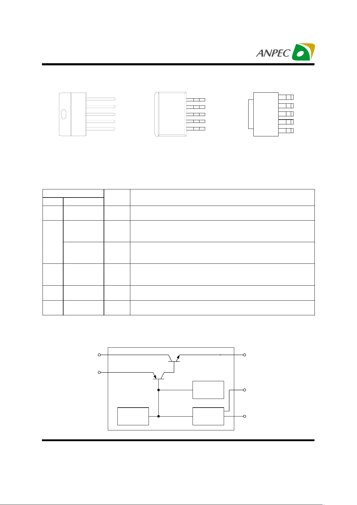
PIN
No. Name
I/O Description
1V
SENSE
I
Positive side of the refere nce voltage , which allows remote s ensing to
obtain excellent load regulatio n.
ADJ O
Negative side of the reference voltage, which allows to use resistor
divider to set an expect output voltage. A small bypass capacitor can be
connected from this pin to ground to improve PSRR performance.
2
GND O
For fixed voltage devices this is the bottom of the resistor divider that
sets the output voltage.
3V
OUT
O
Output pin of the regulator, which connects to the TAB. A minim um of
10µF capacitor must be connected from this pin to ground to ensure the
stability.
4V
CONTROL
I
Supply pin of the control cir cuitry, Which must be always higher than
V
OUT
for the device to regulate. (see electrical characteristics)
5VINI
Power input pin of the regulator, which must be always higher than
V
OUT
for the device to regulate. (see electrical characteristics)
Block Diagram
Pin Configuration
Pin Description
Current
Limit
Voltage
Regulation
Thermal
Protection
V
IN
V
CONTROL
V
OUT
ADJ/GND
V
SENSE
V
SENSE
ADJ(or G ND)
V
OUT
V
CONTROL
V
IN
1
2
3
4
5
TAB is V
OUT
V
SENSE
ADJ(or GND)
V
OUT
V
CONTROL
V
IN
1
2
3
4
5
TAB is V
OUT
Front View of TO-220-5 Front View of TO-263-5
V
IN
V
CONTROL
V
OUT
ADJ(or GND)
V
SENSE
1
2
3
4
5
TAB is V
OUT
Front View of TO-252-5
Copyright ANPEC Electronics Corp.
Rev. A.8- Oct., 2003
APL1581
www.anpec.com.tw3
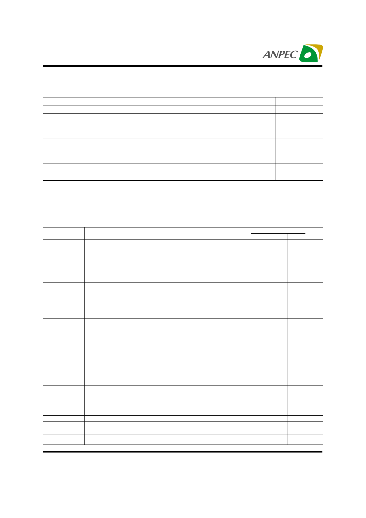
Symbol Parameter Rating Unit
V
IN
Input Voltage 7 V
V
CONTROL
Co n trol Volta g e 13.2 V
Q
JA
Thermal Resistance – Junction to Ambient 62.5
°C/W
P
D
Pow e r D is sip a tio n Intern a lly L im ite d W
T
J
Operating Junction Tem p erature
°C
Control Section 0 to 125
Power Transistor 0 to 150
T
STG
Storage Temperature Range -65 to +150
°C
T
L
Lead Temperature (Soldering, 10 second) 260
°
C
Absolute Maximum Ratings
Electrical Characteristics
Unless otherwise noted , these specifications apply over CIN=10uF , CCONTROL=1uF , COUT=10uF , and
TJ=0 to 125°C. Typical values refer to TJ=25°C. VOUT=VSENSE.
APL1581
Symbol Parameter Test Conditions
MIN TYP MAX
UNIT
V
REF
Reference Voltage
APL1581 V
CONTROL
=2.75~12V, VIN=2.05~5.5V,
I
O
=10mA~5A, V
ADJ
=0V
1.225 1.250 1.275 V
V
OUT
Output Voltage
APL1581-15
APL1581-18
APL1581-25
(I
O
=0~5A for fixed versions)
V
CONTROL
=3~12V , VIN=2.3~5.5V
V
CONTROL
=3.3~12V , VIN=2.6~5.5V
V
CONTROL
=4~12V , VIN=3.3~5.5V
1.470
1.764
2.450
1.500
1.800
2.500
1.530
1.836
2.550
V
REG
LINE
Line Regulation
APL1581
APL1581-15
APL1581-18
APL1581-25
(IO =0A for fixed versions)
V
CONTROL
=2.75~12V, VIN=1.75~5.5V,
I
O
=10mA, V
ADJ
=0V
V
CONTROL
=3~12V, VIN=2.3~5.5V
V
CONTROL
=3.3~12V, VIN=2.6~5.5V
V
CONTROL
=4~12V, VIN=3~5.5V
3mV
REG
LOAD
Load Regulation (note 1)
APL1581
APL1581-15
APL1581-18
APL1581-25
(IO =0~5A for fixed versions)
V
CONTROL
=2.75V, VIN=2.1V, V
ADJ
=0V,
I
O
=10mA~ 5A
V
CONTROL
=3V, VIN=2.35V
V
CONTROL
=3.3V, VIN=2.65V
V
CONTROL
=4V, VIN=3.35V
5mV
V
CONTROL-VOUT
Dropout Voltage (note 2)
APL1581
APL1581-15
APL1581-18
APL1581-25
I
O
=5A for all versions
V
IN
=2.05V, V
ADJ
=0V
V
IN
=2.3V
V
IN
=2.6V
V
IN
=3.3V
1.20 1.35 V
VIN-V
OUT
Dropout Voltage (note 2)
APL1581
APL1581-15
APL1581-18
APL1581-25
I
O
=5A for all versions
V
CONTROL
=2.75V, V
ADJ
=0V
V
CONTROL
=3V
V
CONTROL
=3.3V
V
CONTROL
=4V
0.52 0.75 V
I
LIMIT
Current Limit V
CONTROL-VOUT
=1.5V, VIN-V
OUT
=0.6V 5 A
I
LMIN
Minimum Load C urrent
(note 3) APL1581 V
CONTROL
=5V, VIN=3.3V, V
ADJ
=0V
0.8 10 m A
REG
THERMAL
Thermal Regulation 30mS P ulse 0.01
%
/W
Copyright ANPEC Electronics Corp.
Rev. A.8- Oct., 2003
APL1581
www.anpec.com.tw4
Note 1 : Low duty cycle pulse test with Kelvin connections are required to maintain data accuracy .
Note 2 : Dropout voltage is defined as the minimum
difference between VIN and VOUT required to maintain
1% VOUT regulation .
Note 3 : Minimum load current is defined as the minimum current required at the output to maintain VOUT
regulation.
Application Circuit
∗ VOUT = VREF ( 1+ R2 / R1 ) + IADJ * R2
∗ R1 is typically in range of 100Ω to 125Ω to satisfy the minimum load current requirement
V
SENSE
V
OUT
V
IN
APL1581
ADJ
V
CONTROL
GND
2.5V
GND
5.0V
3.3V
5
4
2
1
3
R2
125
Ω
R1
125
Ω
V
REF
-+
APL1581
Symbol Parameter Test Conditions
MIN TYP MAX
UNIT
PSRR
Power Supply Ripple
Rejection
APL1581
APL1581-15
APL1581-18
APL1581-25
V
RIPPLE
=1VPP at 120Hz, IO=5A
V
CONTROL
=5V, VIN=5V, V
ADJ
=0V
V
CONTROL
=5.25V, VIN=5.25V
V
CONTROL
=5.55V, VIN=5.55V
V
CONTROL
=6.25V, VIN=6.25V
60 70 dB
I
CONTROL
Control Pin Current
V
CONTROL-VOUT
=1.5V , VIN-V
OUT
=0.8V,
I
O
=5A
45 120 mA
I
GND
Ground Pin Current
APL1581-15
APL1581-18
APL1581-25
V
CONTROL
=3V, VIN=2.3V
V
CONTROL
=3.3V, VIN=2.6V
V
CONTROL
=4V, VIN=3.3V
813mA
I
ADJ
Adjust Pin Current
APL1581 V
CONTROL
=2.75V , VIN=2.05V , V
ADJ
=0V
50 120
µ
A
Q
JC
Junction-to-Case
Thermal Resistance
Power Transistor 3.0 °C/W
Unless otherwise noted , these specifications apply over CIN=10uF , CCONTROL=1uF , COUT=10uF , and
TJ=0 to 125°C. Typical values refer to TJ=25°C. VOUT=VSENSE.
Electrical Characteristics Cont.

Copyright ANPEC Electronics Corp.
Rev. A.8- Oct., 2003
APL1581
www.anpec.com.tw5
Application Circuit
V
SENSE
V
OUT
V
IN
APL1581-25
GND
V
CONTROL
GND
2.5V
GND
5.0V
3.3V
5
41
3
 Loading...