

APC308
Rail to Rail Output CMOS Operating Amplifier
Features
••
•
Operating Voltage
••
Single Supply 3V to 6V
• Low Input current 2pA
••
•
Rail to Rail Output Swing
••
••
•
Push-Pull Output Driving
••
••
•
High Output Current Drive 310mA
••
••
• Bandwidth:7MHz
••
••
• Wide Temperature Range
••
••
• Available in 8 pin SOP ,DIP , TSSOP or MSOP
••
Package
Ordering Information
Applications
• Amplifiers
• Filters
• Analog circuit
Gereral Description
The APC308 consists of two independent, high gain,
CMOS operating amplifier, combining rail to rail output range with large output current. It provides a low
input bias current 2pA.
The output swing of the amplifier, guaranteed for
loads down to 1kΩ and output current to an 10Ω load
from a 5V power supply. APC308 designed to operating at 3V is especially well-suited for low voltage
application.
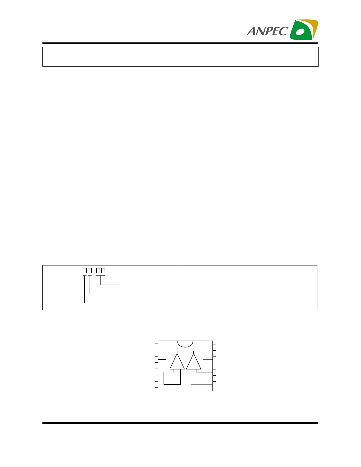
)2+!&
Handling Code
Temp. Range
Package Code
Package Code
J : PD IP - 8 K : SO P - 8
O : TSSO P - 8 X : MSOP-8
Temp. Range
I : - 40 to 85 C
Handling Code
TU : T ube T R : Ta pe & Reel
°
Block Diagram
Out 1
Inverting Inpu t 1
Non-inverting Input 1
+
!
"
V
--
--+
APC308
ANPEC reserves the right to make changes to improve reliability or manufacturability without notice, and advise
customers to obtain the latest version of relevant information to verify before placing orders.
Copyright ANPEC Electronics Corp.
Rev. A.1 - Oct., 2001
&
V
,,
%
Out 2
$
Inverting Input 2
#
Non-inverting Input 2
www.anpec.com.tw1
APC308
Absolute Maximum Ratings
Symbol Parameter Rating Unit
V
DD
T
SC(O)
T
A
T
J
T
STG
T
S
V
ESD
Note : *1. Human body model : C=100pF , R=1500Ω , 3 positive pulses plus 3 negative pulses
Thermal Characteristics
Symbol Parameter Value Unit
R
THJA
Supply Voltage 7 V
Output Short-circuit duration, at TA=25°C, P
=1W 20 S
TOT
Operating Ambient Temperature range -40 to 85 °C
Maximum Junction Temperature 150 °C
Storage Temperature Range -65 to +150 °C
Soldering Temperature, 10 seconds 260 °C
Electrostatic Discharge -3000 to 3000
*1
Thermal Resistance from Junction to Ambient in Free Air
DIP-8
SO-8
TSSOP
MSOP
109
180
220
220
V
K/W
K/W
K/W
K/W
Electrical Characteristics
VDD=5V , TA=25°C (unless otherwise noted)
Symbol Parameter Condition Min. Typ. Max. Unit
Vos Input Offset Voltage
Ibias Input Bias Current Ta=25°C 2 pA
Vicm
R
Input Common Mode Voltage
Range
Input Resistance 5
IN
Vo Output Voltage Swing
Voh Output Voltage High
Vol Output Voltage Low
lout
Output Current Source Vo=4.5V -310 mA
Output Current Sink Vo=0.5V 370 mA
CMRR Common Mode Rejection Ratio -80 dB
Copyright ANPEC Electronics Corp.
Rev. A.1 - Oct., 2001
Ta =2 5° C 4 1 0 mV
-25°C<Ta<75°C 5 mV
Ta =2 5° C 0 VDD-0.8 V
M
=2k
R
Ω
L
R
=10kΩ,
L
-25°C<Ta<75°C
=10kΩ,
R
L
-25°C<Ta<75°C
05V
5V
0V
www.anpec.com.tw2
Ω

APC308
Electrical Characteristics Cont.
VDD=5V , TA=25°C (unless otherwise noted)
Symbol Parameter Condition Min. Typ. Max.
PSRR Supply Voltage Rejection Ratio
Av Large Signal Voltage Gain 85 dB
GBW Gain Bandwidth Product 7 MHz
SR Slew Rate 5.6
Icc Supply Current
Vrr=100mVpp,
fin=100H
-25°C<Ta<75°C 2.0 4 mA
2.4V<Vcc<6V,
Ta =2 5° C
Z,RL
=2k
Ω
-50 dB
2.5 5 mA
Unit
V/µs
Copyright ANPEC Electronics Corp.
Rev. A.1 - Oct., 2001
www.anpec.com.tw3

APC308
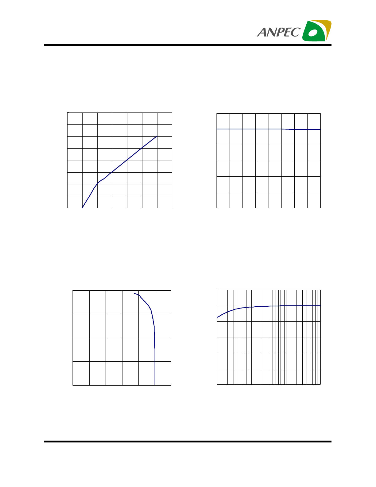
Typical Characteristics
Supply Current vs Supply Voltage
No Load
4
3.5
3
2.5
2
1.5
1
Supply Current (mA)
0.5
0
0123 4567
Supply voltage(V)
Input Offset Voltage vs Temperature
VDD=5V
Supply Current vs Temperature
VDD=5V
2.0
1.8
1.6
1.4
1.2
1.0
0.8
0.6
Supply Current (mA)
0.4
0.2
0.0
-25 0 25 50 75
Temperature(°C)
Input Common Mode Voltage vs Supply
Voltage
7
6
5
4
3
VOS (mV)
2
1
0
-25 0 25 50 75
Temperature(°C)
Copyright ANPEC Electronics Corp.
Rev. A.1 - Oct., 2001
6
5
4
3
VICM (V)
2
1
0
01234567
Supply Voltage(V)
www.anpec.com.tw4
APC308
Typical Characteristics
Output Swing vs Supply Voltage
RL=2kΩ
8
7
6
5
4
3
Output Swing (V)
2
1
0
01234567
Supply Voltage (V)
Output Swing (V)
Output Swing vs Temperature
VDD=5V, RL=2kΩ
6
5
4
3
2
1
0
-25 0 25 50 75
Temperature(°C)
Output Current vs Output Swing Output Swing vs Load Resistance
VDD=5V
1000
100
10
Output Swing (mA)
1
0.1
0123456
Output Swing (V)
Copyright ANPEC Electronics Corp.
Rev. A.1 - Oct., 2001
VDD=5V
6
5
4
3
2
Output Swing (V)
1
0
10 100 1k 10k
Load Resistance (Ω)
www.anpec.com.tw5

APC308
Typical Characteristics
Sink Current vs Output Voltage
VDD=5V VDD=5V
500
450
400
350
300
250
200
150
Sink Current (mA)
100
50
0
0 0.1 0.2 0 .3 0.4 0.5 0.6 0.7 0.8 0.9 1
500
450
400
350
300
250
200
150
Source Current (mA)
100
50
0
0 0.1 0.2 0.3 0.4 0.5 0 .6 0.7 0 .8 0.9 1
Output Voltage Referred to Ground (V)
Large Signal Voltage Gain vs Frequency
VDD=5V
+100
+90
+80
Large Signal Frequency Response
VDD=5V, RL=2kΩ
6
5
Source Current vs Output Voltage
Output Voltage Referred to Vdd(V)
+70
+60
+50
Av (dB)
+40
+30
+20
+10
+0
10
100 1k 10k 100k 1M
Frequency (Hz)
Copyright ANPEC Electronics Corp.
Rev. A.1 - Oct., 2001
10M
4
3
2
Output Swing (V)
1
0
10 100 1k 10k 100k 1M 10M
Frequency (Hz)
www.anpec.com.tw6

APC308
Typical Characteristics
Large Signal Voltage Gain vs Supply
Voltage
100
95
90
85
80
75
Av (dB)
70
65
60
55
50
12345
Supply Voltage (V)
PSRR vs Frequency
VDD=5V
VRR=100mVpp/100Hz
+0
-10
-20
-30
-40
PSRR (dB)
-50
-60
CMRR vs Frequency
VDD=5V,RL=10kΩ
+0
-10
-20
-30
-40
-50
-60
CMRR (dB)
-70
-80
-90
-10 0
10 100k100 1k 10k
Frequency (Hz)
Voltage Follower Pulse Response
VDD=5V,RL=2kΩ
9
8
7
6
5
4
3
Output Voltage (V)
2
5
4
3
2
1
0
-1
Input Voltage (V)
-2
-70
-80
10 100k100 1k 10k
Frequency (Hz)
Copyright ANPEC Electronics Corp.
Rev. A.1 - Oct., 2001
1
0
!"#
Time (µs)
www.anpec.com.tw7
-3
-4

APC308
Typical Characteristics
Voltage Follower Pulse Response
VDD=5V,CL=270pF
0.5
0.4
0.3
0.2
0.1
Output Voltage (V)
-0.1
-0.2
0.2
0.1
0
-0.1
-0.2
0
12034
-0.3
-0.4
-0.4
-0.5
Input Voltage (V)
Time (µs)
Copyright ANPEC Electronics Corp.
Rev. A.1 - Oct., 2001
www.anpec.com.tw8

APC308
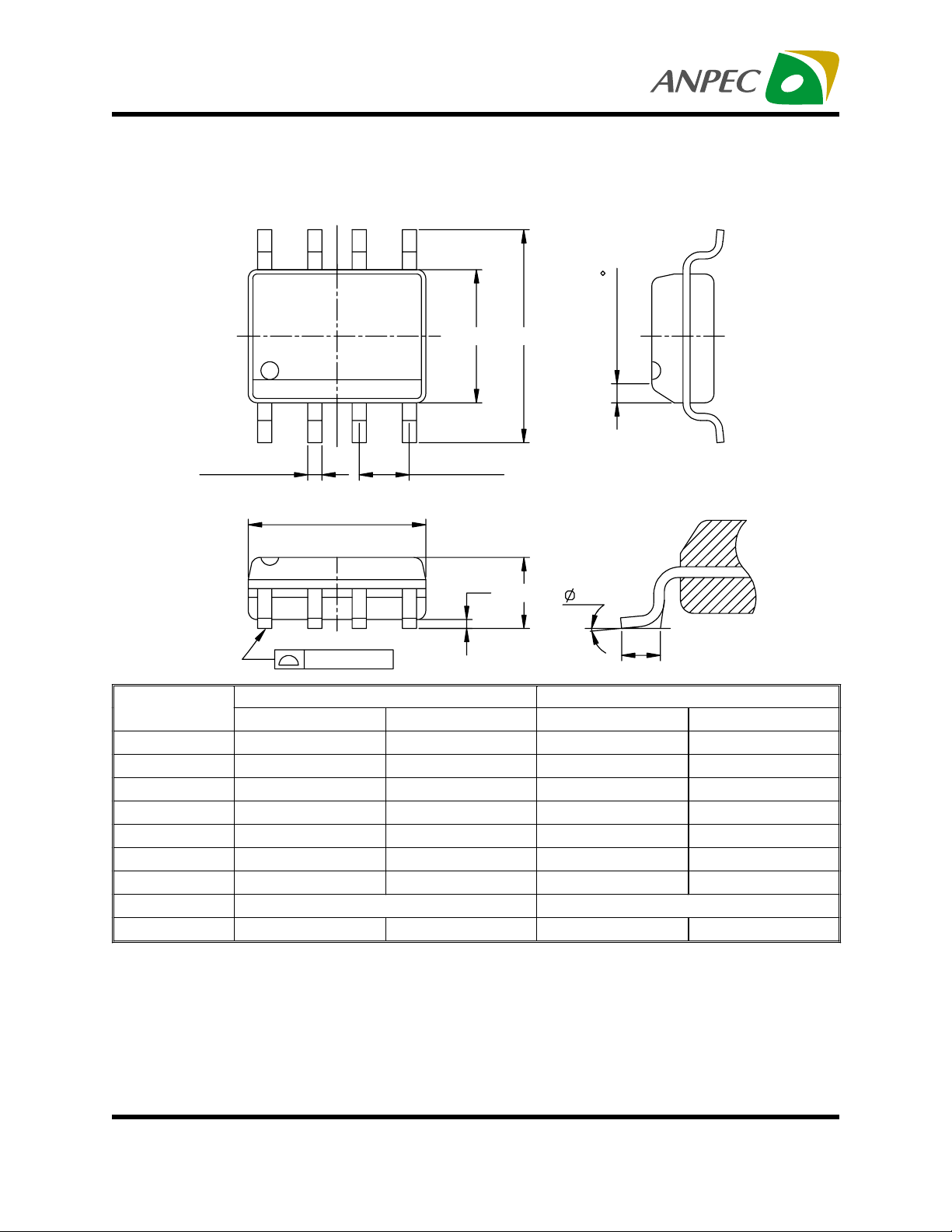
Packaging Information
PDIP-8 pin ( Reference JEDEC Registration MS-001)
D
1
A
L
e2
e 3
Dim
A
A1
A2
D
e1
e2
e3
E
E1
E3
L
1 0
φ
e 1
A1
E1
A2
1
E
E3
Millimeters Inches
Min. Max. Min. Max.
5.33 0.210
0.38 0.015
2.92 3.68 0.115 0.145
9.02 10.16 0.355 0.400
2.54BSC 0.100BSC
0.36 0.56 0.014 0.022
1.14 1.78 0.045 0.070
7.62 BSC
8.26
0.300 BSC
0.325
6.10 7.11 0.240 0.280
10.92 0.430
2.92 3.81 0.115 0.150
°
15
°
0
°
15
°
Copyright ANPEC Electronics Corp.
Rev. A.1 - Oct., 2001
www.anpec.com.tw9
APC308
Packaging Information
SOP-8 pin ( Reference JEDEC Registration MS-012)
HE
0.015X45
e1 e2
D
A1
A
1
L
0.004max.
Dim
A 1.35 1.75 0.053 0.069
A1 0.10 0.25 0.004 0.010
D 4.80 5.00 0.189 0.197
E 3.80 4.00 0.150 0.157
H 5.80 6.20 0.228 0.244
L 0.40 1.27 0.016 0.050
e1 0.33 0.51 0.013 0.020
e2 1.27BSC 0.50BSC
1 0
φ
Millimeters Inches
Min. Max. Min. Max.
°
8
°
0
°
8
°
Copyright ANPEC Electronics Corp.
Rev. A.1 - Oct., 2001
www.anpec.com.tw10

APC308
φ
φ
φ
Packaging Information
TSSOP
e
8
7
2 x E / 2
(2)
S
(L1)
GAUGE
PLANE
L
1
Dim
12
b
E1 E
e/2
D
A2
A
A1
0.25
(3)
Millimeters Inches
Min. Max. Min. Max.
A 1.2 0.047
A1 0.00 0.15 0.000 0.006
A2 0.80 1.05 0.031 0.041
b 0.19 0.30 0.007 0.012
D 2.9 3.1 0.114 0.122
e 0.65 BSC 0.026 BSC
E 6.40 BSC 0.252 BSC
E1 4.30 4.50 0.169 0.177
L 0.45 0.75 0.018 0.030
L1 1.0 REF 0.039REF
R 0.09 0.004
R1 0.09 0.004
S 0.2 0.008
10
212
312
°
REF 12° REF
°
REF 12° REF
°
8
°
0
°
8
°
Copyright ANPEC Electronics Corp.
Rev. A.1 - Oct., 2001
www.anpec.com.tw11

APC308
Packaging Information
MSOP
e1
E
e1
A1
Dim
A1 0.06 0.15 0.002 0.006
A2 0.86 TYP 0.34 TYP
A3 0.25 0.4 0.01 0.0126
e 0.65 TYP 0.0256TYP
e1 2.90 3.1 0.114 0.124
E 4.8 5.0 0.189 0.197
E1 2.90 3.1 0.169 0.177
L1 0.25 REF 0.039REF
L2 0.0375 REF 0.953 REF
Min. Max. Min. Max.
Millimeters Inches
A3
E1
A2
L2
L1
Copyright ANPEC Electronics Corp.
Rev. A.1 - Oct., 2001
www.anpec.com.tw12

APC308
Physical Specifications
Terminal Material Solder-Plated Copper (Solder Material : 90/10 or 63/37 SnPb
Lead Solderability Meets EIA Specification RSI86-91, ANSI/J-STD-002 Category 3.
Packaging 2500 devices per reel
Reflow Condition (IR/Convection or VPR Reflow)
Reference JEDEC Standard J-STD-020A APRIL 1999
Peak temperature
temperature
Pre-heat temperature
°
183 C
Time
Classificatio n R e flo w P r of ile s
Convection or IR/
Convection
Average ramp-up rate(183°C to Peak) 3°C/second max. 10 °C /second max.
Preheat temperature 125 ± 25°C)
Temperature maintained above 183°C
Time within 5°C of actual peak temperature
Peak temperature range
Ramp-down rate
Time 25°C to peak temperature
120 seconds max
60 150 seconds
10 20 seconds 60 seconds
220 +5/-0°C or 235 +5/-0°C 215-219°C or 235 +5/-0°C
6 °C /second max. 10 °C /second max.
6 minutes max.
VPR
Package Reflow Conditions
pkg. thickness ≥≥≥≥ 2.5mm
and all bgas
Convection 220 +5/-0 °C Convection 235 +5/-0 °C
VPR 215-219 °C VPR 235 +5/-0 °C
IR/Convection 220 +5/-0 °C IR/Convection 235 +5/-0 °C
Copyright ANPEC Electronics Corp.
Rev. A.1 - Oct., 2001
pkg. thickness < 2.5mm and
pkg. volume ≥≥≥≥ 350 mm³
pkg. thickness < 2.5mm and pkg.
volume < 350mm³
www.anpec.com.tw13
APC308
Reliability test pro gram
Test item Method Description
SOLDERABILITY MIL-STD-883D-2003
HOLT MIL-STD-883D-1005.7
PCT JESD-22-B, A102
TST MIL-STD-883D-1011.9
ESD MIL-STD-883D-3015.7 VHBM > 2KV, VMM > 200V
Latch-Up JESD 78 10ms , IJH > 100mA
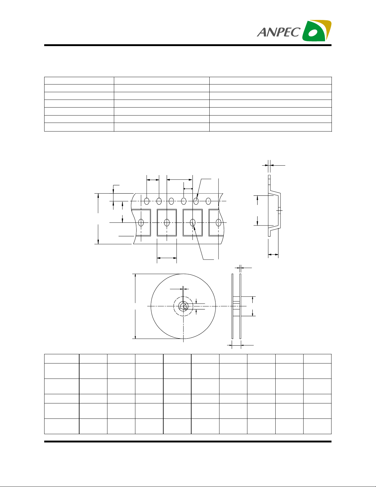
Carrier Tape & Reel Dimensions
245°C , 5 SEC
1000 Hrs Bias @ 125 °C
168 Hrs, 100 % RH , 121°C
-65°C ~ 150°C, 200 Cycles
t
W
E
F
Po P
P1
Ao
J
A
D
Bo
Ko
D1
T2
C
B
T1
Application
SOP- 8
TSSOP- 8
Application
SOP- 8 5.5 ± 0.1 1.55 ± 0.1
TSSOP- 8
Copyright ANPEC Electronics Corp.
Rev. A.1 - Oct., 2001
A B C J T1 T2 W P E
330 ± 1 62 ± 1.5
330 ± 1 62 ± 1.5
F D D1 Po P1 Ao Bo Ko t
5.5 ± 0.
1.5 + 0.1 1.5 + 0.1
12.75
+0.1 5
12.75
0.1 5
±
1.5+0.25
2 + 0.5 12.4 + 0.2
2 + 0.5 12.4 + 0.2
4.0 ± 0.1 2.0 ± 0.1 6.4 ± 0.1 5.2 ± 0.1 2.1 ± 0.1
4.0 ± 0.1 2.0 ± 0.1 7.0 ± 0.1 3.6 ± 0.3 1.6 ± 0.1
2 ± 0.2
2 ± 0.2
12 + 0.3
- 0.1
12 + 0.3
- 0.1
8.0 ± 0.1 1.75 ± 0.1
8.0 ± 0.1
www.anpec.com.tw14
.75 ± 0.1
0.3
0.013
±
0.3
0.013
±
(mm)

APC308
Cover Tape Dimensions
Carrier Width
Cover Tape Width
Customer Service
Anpec Electronics Corp.
Head Office :
5F, No. 2 Li-Hsin Road, SBIP,
Hsin-Chu, Taiwan, R.O.C.
Tel : 886-3-5642000
Fax : 886-3-5642050
Taipei Branch :
7F, No. 137, Lane 235, Pac Chiao Rd.,
Hsin Tien City, Taipei Hsien, Taiwan, R. O. C.
Tel : 886-2-89191368
Fax : 886-2-89191369
12
9.3
(mm)
Copyright ANPEC Electronics Corp.
Rev. A.1 - Oct., 2001
www.anpec.com.tw15
 Loading...