

ANPEC APL5833-33DC-TR, APL5833-28EC-TU, APL5833-28DC-TU, APL5833-28DC-TR, APL5833-EC-TR Datasheet
...
APL5833
300mA Low Dropout Linear Regulator of Fixed 2.85V,3.3V and 3.5V
Features General Description
••
•
Low Dropout Voltage of 1.2V at 300mA
••
••
•
Output Voltage Accuracy ± 2.0%
••
••
•
Line Regulation - 1mV (typ.)
••
••
• Load Regulation - 6mV (typ.)
••
••
• Input Voltage Range up to 9V
••
••
• Internal Current Limiting and Thermal Shut-
••
down Protections
••
• Available Output Voltages - 2.85V, 3.3V and
••
3.5V
••
• Various SOT-89 and TO-92 Packages Avail-
••
able
Applications
• Voltage Regulator for CD-ROM Drivers
• Voltage Regulator for LAN Cards
• Wireless Communication Systems
The APL5833 is a 3-pin low dropout linear regulator
with 2.0% accuracy of output voltage over line, load
and temperature variations. Dropout voltage at
300mA output current is less than 1.2V. Both output
current limiting and thermal shutdown are built in to
provide maximal protection to the APL5833 against
fault conditions. The over current and thermal shutdown circuits become active when the current exceed 300mA, or the junction temperature reach
150°C. Normal operation is recovered when junction
temperature drops below 130°C.
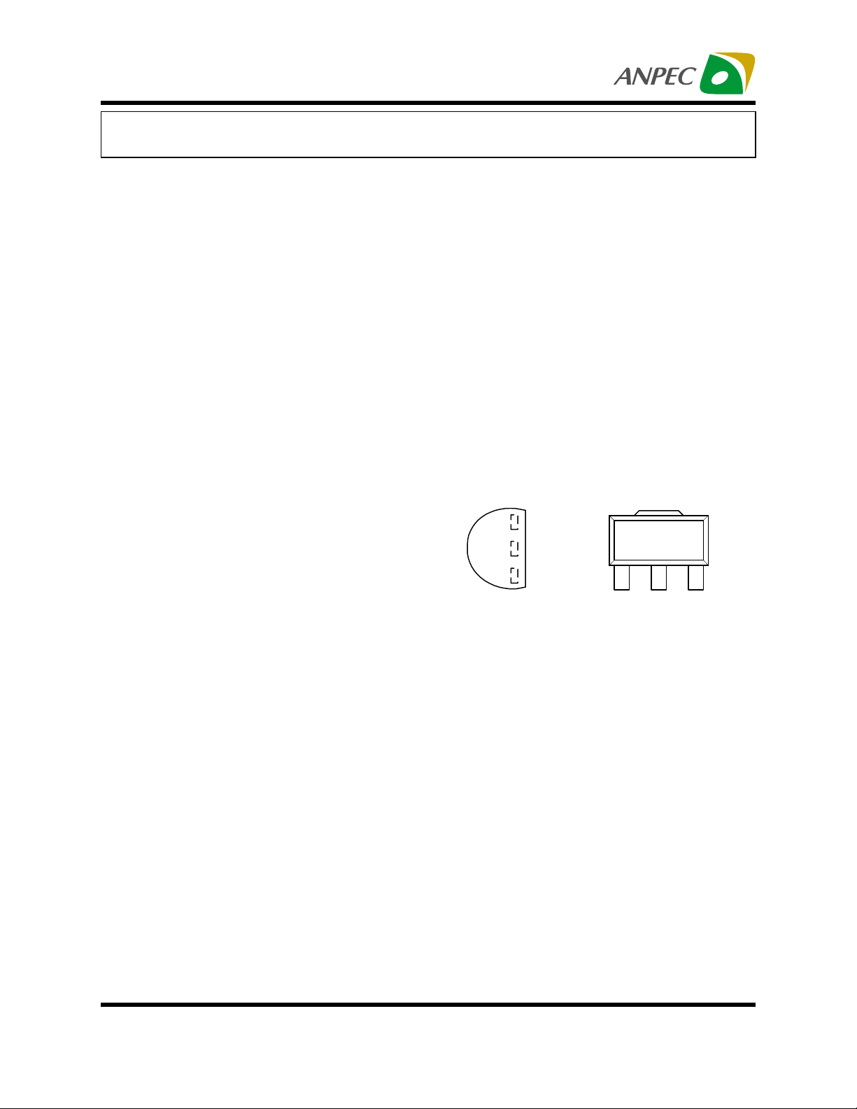
Pin Configuration
V
3
IN
2
GND
V
1
OUT
TO-92 (Top View)
SOT-89 (Top View)
213
V
GND
OUT
V
IN
• Portable Instrument
• Portable Consumer Equipment
• Low Voltage Systems
ANPEC reserves the right to make changes to improve reliability or manufacturability without notice, and advise
customers to obtain the latest version of relevant information to verify before placing orders.
Copyright ANPEC Electronics Corp.
Rev. B.1 - Apr., 2003
www.anpec.com.tw1
APL5833
Ordering and Marking Information
APL5833-
Handling Code
Tem p. Range
Package Code
Voltage Code
AP L5833 D :
AP L5833 -28 D : XXXXX - Date CodeAP L5833-28 E :
AP L5833 -33 D :
AP L5833 -35 D :
APL5833
XXXXX
APL5833
XXXXX28
APL5833
XXXXX33
APL5833
XXXXX35
XXXXX - Date Code
XXXXX - Date Code
XXXXX - Date Code
XXXXX - Date Code
Package Code
D : S O T - 8 9 E : T O - 9 2
Tem p. Range
C : 0 to 70 C
Handling Code
TU : Tube TR : Tape & Reel
Voltage Code
28 : 2.85V 33 : 3.3V
35 : 3.5V B lank : Adjustable Version
AP L5833 -33 E :
AP L5833 -35 E :
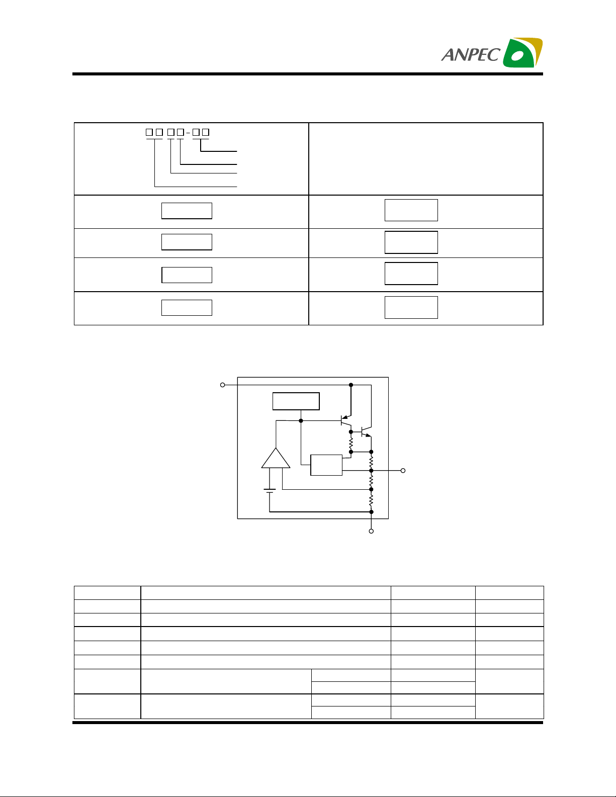
Block Diagram
V
IN
Thermal
Shutdown
°
APL
5833
XXXXX
APL
5833
XXXXX28
APL
5833
XXXXX33
APL
5833
XXXXX35
XXXXX - Date CodeAP L5833 E :
XXXXX - Date Code
XXXXX - Date Code
-
+
V
REF
Current
Limit
GND
V
OUT
Absolute Maximum Ratings
Symbol Parameter Rating Unit
V
IN
I
OUT
T
A
T
J
T
STG
D
θ
JA
Copyright ANPEC Electronics Corp.
Rev. B.1 - Apr., 2003
Input Voltage 9 V
Output Current 450 mA
300
Operating Am bient Temperat ure Range 0 to 70
Operating Junction Temperature Range -40 to +150
Storage Temperature Range -65 to +150
Power Dissipation Package
SOT-89 550P
TO-92 550
Thermal Resistance
SOT-89 180
TO-92 180
www.anpec.com.tw2
C
°
C
°
C
°
mW
C / W
°
APL5833
Electrical Characteristics (T
=25°C, unless otherwise noted)
A
Symbol Parameter Test Conditions
V
Input Voltage V
IN
V
I
REG
REG
V
DROPOUT
PSRR
OTS
Output Voltage I
OUT
Output Cur ren t
OUT
Capability
I
Short Circuit Current
SC
I
Quiescent C ur ren t V
Q
Line Regulation I
LINE
Load Regulation I
LOAD
Dropout Voltage
Power Supply Rejection
Ratio
=10mA 0.98 V
OUT
V
=3.3V, ∆ V
OUT
V
0.4V
<
OUT
=5V, No Load 6 10 mA
IN
=10mA, VIN= 5V to 8V 1 6 mV
OUT
=1mA~3 00mA 6 12 mV
OUT
=300mA, ∆ V
I
OUT
OUT
OUT
at 1kHz 55 dB
Over Temperature
Shutdown
E
Output Noise 100
N
Output Voltage
TC
Temperature Coefficient
=2%
=1%
APL5833
Min. Typ. Max.
+1.2V 9 V
OUT
OUT
1.02 V
OUT
300 mA
500 mA
1200 1300 mV
150 °C
100 ppm/°C
Unit
Vrms
µ
V
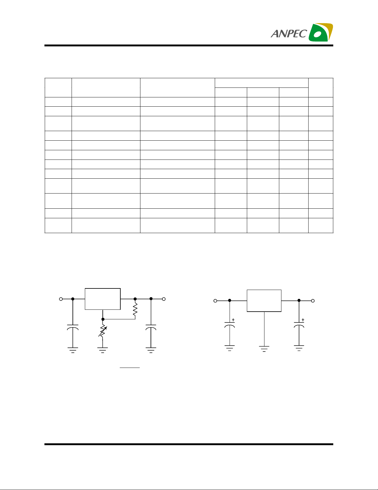
Application Schematic
1.25V to 7V Adjustable Regulator
APL5833
V
IN
+
1µF
OUT
ADJ
1.250VV
OUTIN
R1
+
R2
+
R2R1
×=
R1
10µ
Fixed 2.85, 3.3V and 3.5V Regulator
APL5833
V
OUT
F
V
IN
1µF
OUTIN
GND
10µ
V
OUT
F
Copyright ANPEC Electronics Corp.
Rev. B.1 - Apr., 2003
www.anpec.com.tw3
APL5833
5
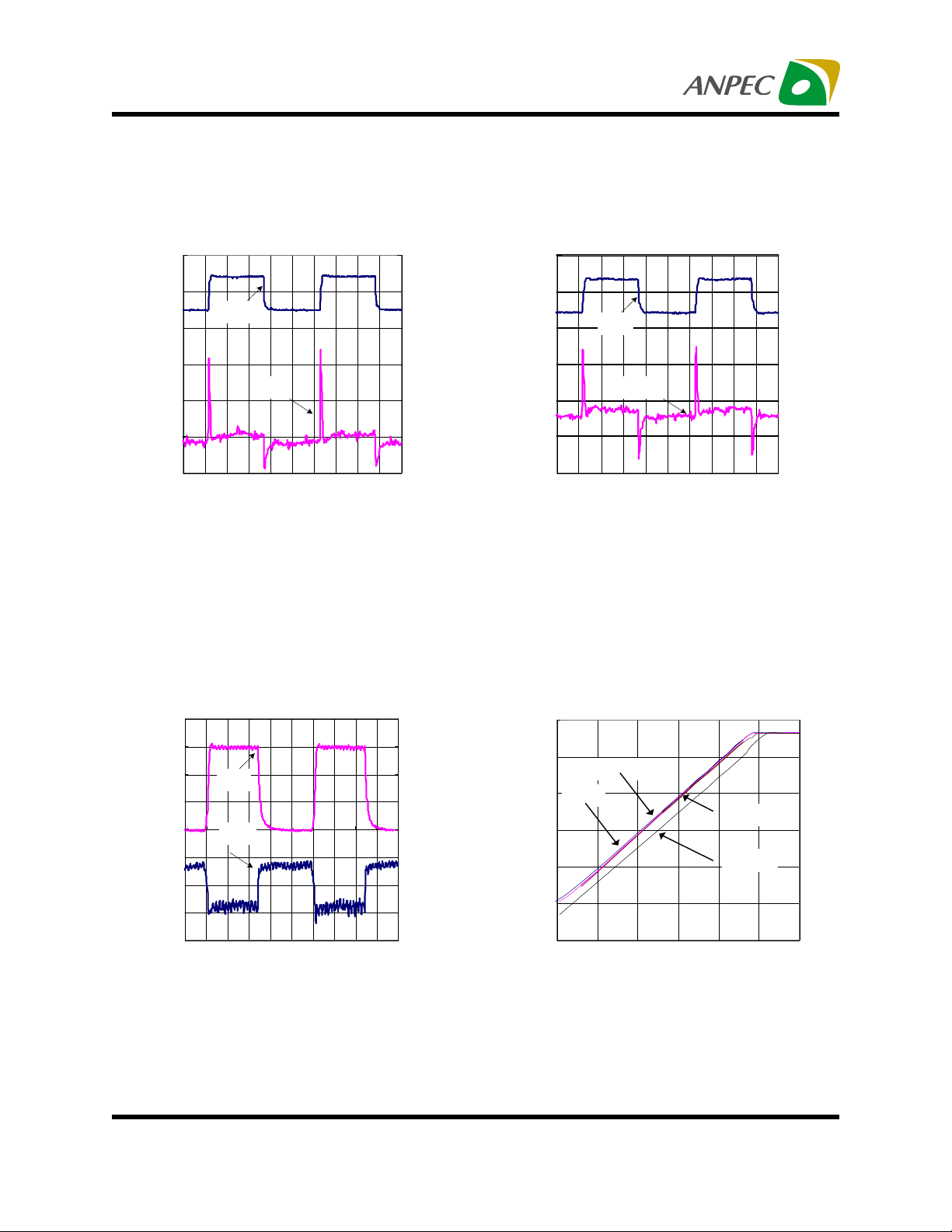
Typical Characteristics
Line Transient Response
6
5
4
3
2
1
0
Input Voltage (V)
0102030405060708090100
V
IN
V
(CL=1µF, I
OUT
Time (ns)
OUT
=1mA)
25
20
15
10
5
0
-5
Line Transient Response
6
5
4
3
2
1
Output Voltage (mV)
0
Input Voltage (V)
0102030405060708090100
V
IN
V
OUT
Time (ns)
(CL=10µF, I
=10mA)
OUT
20
10
0
-10
Output Voltage (mV)
Load Transient Response
(C
=10µF, VIN=5V)
0.4
L
0.3
0.2
V
IN
0.1
0
V
OUT
-0.1
-0.2
-0.3
Output Current (A)
-0.4
-200 200 600 1000 1400 1800
Time (ns)
30
25
20
15
10
5
0
-5
-10
Output Voltage vs. Input Voltage
3.5
3
2.5
10mA
1mA
2
1.5
1
Output Voltag (V)
0.5
2 2.5 3.5 4 4.5
3
Input Voltage (V)
50mA
300mA
Copyright ANPEC Electronics Corp.
Rev. A.7 - Apl., 2001
www.anpec.com.tw4

APL5833
Typical Characteristics (Cont.)
Output Voltage vs. Input Voltage Input Current vs. Input Voltage
3.35
3.33
8
7
6
3.31
3.29
3.27
Output Voltage (V)
3.25
5678910
5
4
3
2
1
Input Current (mA)
0
0246810
Input Voltage (V) Input Voltage (V)
Short Current vs. Input Voltage Output Voltage vs. Output Current
700
600
3.35
3.33
500
400
300
200
100
Short Current (mA)
0
02 4 6 810
Copyright ANPEC Electronics Corp.
Rev. A.7 - Apl., 2001
3.31
3.29
3.27
Output Voltage (V)
3.25
0 100
Output Current (mA)Input Voltage (V)
200 300
www.anpec.com.tw5

APL5833
Typical Characteristics (Cont.)
Dropout Voltage vs. Output Current
1240
1220
1200
1180
1160
1140
1120
1100
1080
1060
Dropout Voltage (mV)
0 50 100 150 200 250 300
Output Current (mA)
Output Voltage vs. Temperature
3.35
3.34
3.3
3.32
3.31
3.30
3.29
3.28
3.27
3.26
Output Voltage (V)
3.25
-50
0
50 100
Temperature (°C)
150
Short Current vs. Temperature
550
540
530
520
510
500
490
480
Short Current (mA)
-50 0
50 100
Temperature ( °C)
Input Current vs. Temperature
9
8
7
6
5
4
3
2
1
Short Current (mA)
0
-50 0
50
Temperature ( °C)
100
150
150
Copyright ANPEC Electronics Corp.
Rev. A.7 - Apl., 2001
www.anpec.com.tw6

APL5833
Packaging Information
TO-92
3
J
e
e1
L1
Q
A
L2
SEATING PLANE
b2
L
b
2
1
S
E
S
Millimeters Inches
Dim
Min. Max. Min. Max.
A 4.58 5.33 0.170 0.210
φ b
φ b2
φ D
0.41 0.53 0.160 0.021
0.41 0.48 0.160 0.019
4.96 5.20 0.175 0.205
E 3.94 4.19 0.125 0.165
e 2.42 2.66 0.095 0.105
e1 1.15 1.39 0.045 0.055
J 3.43 0.135
L 12.70 0.500
L1 1.27 0.050
L2 6.35 0.250
Q 2.93 0.115
S 2.42 2.66 0.080 0.105
D
Copyright ANPEC Electronics Corp.
Rev. B.1 - Apr., 2003
www.anpec.com.tw7

APL5833
Packaging Information
SOT-89 (Reference EIAJ ED-7500A Reg stration SC-62)
D
D1
H
L
123
a
E
C
Dim
B1
B
e
e1
A
a
Millim eters Inches
Min. Max. Min. Max.
A 1.40 1.60 0.055 0.063
B 0.40 0.56 0.016 0.022
B1 0.35 0.48 0.014 0.019
C 0.35 0.44 0 .014 0.017
D 4.40 4.60 0 .173 0.181
D1 1.35 1.83 0.053 0.072
e 1.50 BSC 0.059 BSC
e1 3.00 BSC 0.118 BSC
E 2.29 2.60 0.090 0.102
H 3.75 4.25 0 .148 0.167
L 0.80 1 .20 0.031 0.047
α
10
°
10
°
Copyright ANPEC Electronics Corp.
Rev. B.1 - Apr., 2003
www.anpec.com.tw8

APL5833
Physical Specifications
Terminal Material Solder-Plated Copper (Solder Material : 90/10 or 63/37 SnPb)
Lead Solderab ility Meets EIA Specification RSI86 -91, A N SI/J-STD-002 Cate gory 3.
Reflow Condition (IR/Convection or VPR Reflow)
Reference JEDEC Standard J-STD-020A APRIL 1999
Peak temperature
temperature
Pre-heat temperature
Classification Reflow Profiles
Average ramp-up rate(183
Preheat temperature 125± 25°C)
Temperature maintained above 183
Time within 5°C of actual peak temperature
Peak temperature range
Ramp-down rate
Time 25
°
C to peak temperature
°
C to Peak)
°
C
°
3
120 seconds max.
60 ~ 150 seconds
10 ~ 20 seconds
220 +5/-0
°
6
6 minutes max.
°
183 C
Time
Convection or IR/
Convection
C/second max. 10°C /second max.
60 seconds
°
C or 235 +5/-0°C 215~ 219°C or 235 +5/-0°C
C /second max. 10°C /second max.
VPR
pkg. thickness
and all bags
Convection 220 +5/-0°C
VPR 215-219°C
IR/Convection 220 +5/-0°C IR/Convection 235 +5/-0°C
Copyright ANPEC Electronics Corp.
Rev. B.1 - Apr., 2003
≥≥≥≥
2.5mm
pkg. thickness < 2.5mm and
≥≥≥≥
pkg. volume
350 mm
pkg. thickness < 2.5mm and pkg.
volume <
°
Convection 235 +5/-0
VPR 235 +5/-0
°
C
C
www.anpec.com.tw9

APL5833
Reliability test Program
Test item Method Description
SOLDERABILITY MIL-STD-883D-2003
HOLT MIL-STD-883D-1005.7
PCT JESD-22-B, A102
TST MIL-STD-883D-1011.9
ESD MIL-STD-883D-3015.7 VHBM > 2KV, VMM > 200V
Latch-Up JESD 78 10ms , Itr > 100mA
Carrier Tape & Reel Dimensions
°
C , 5 SEC
245
1000 Hrs Bias @ 125
168 Hrs, 100 % RH , 121
°
C ~ 150°C, 200 Cycles
-65
t
°
C
°
C
D1
D
Bo
Ko
T2
B
T1
E
F
W
A
Po
P
P1
Ao
J
C
Applicatio n
SOT-89
Applicatio n
SOT-89
Copyright ANPEC Electronics Corp.
Rev. B.1 - Apr., 2003
A B C J T1 T2 W P E
178 ±1 70 ± 2
F D D1 Po P1 Ao Bo Ko t
5.5 ± 0.05 1.5± 0.1 1.5± 0.1 4.0 ± 0.1 2.0 ± 0.1 4.8 ± 0.1 4.5± 0.1 1.80± 0.1 0.3±0.013
13.5
0.15
±
3 ± 0.15 14 ± 2 1.3 ± 0.3
12 + 0.3
12 - 0.1
8 ± 0.1 1.75± 0.1
(mm)
www.anpec.com.tw10

APL5833
Cover Tape Dimensions
Application Carrier Width Cover Tape Width Devices Per Reel
SOT- 89
Customer Service
Anpec Electronics Corp.
Head Office :
5F, No. 2 Li-Hsin Road, SBIP,
Hsin-Chu, Taiwan, R.O.C.
Tel : 886-3-5642000
Fax : 886-3-5642050
Taipei Branch :
7F, No. 137, Lane 235, Pac Chiao Rd.,
Hsin Tien City, Taipei Hsien, Taiwan, R. O. C.
Tel : 886-2-89191368
Fax : 886-2-89191369
12 9.3 1000
Copyright ANPEC Electronics Corp.
Rev. B.1 - Apr., 2003
www.anpec.com.tw11
 Loading...