


ANPEC APL1541-KC-TU, APL1541-KC-TRL, APL1541-KC-TR, APL1541-33KC-TUL, APL1541-33KC-TU Datasheet
...
APL1541
1A Low Dropout Fast Response Positive Adjustable Regulator and Fixed 3.3V
Features
••
•
Guaranteed Output Voltage Accuracy within 2%
••
••
•
Fast Transient Response
••
••
•
Guaranteed Dropout Voltage at Multiple Cur-
••
rents
••
•
Load Regulation : 0.1% Typ.
••
••
•
Line Regulation : 0.03% Typ.
••
••
• Low Dropout Voltage : 1.1V Typ. at I
••
••
• Current Limit : 1A Typ. at T
••
••
• On-Chip Thermal Limiting : 150 °C Typ.
••
••
• Adjustable Output : 1.25~7.75V
••
••
• Standard 8-pin SO Power Package
••
=125 °C
J
OUT
=1A
Applications
General Description
The APL1541 is a low dropout three-terminal adjustable regulators with 1A output current capability. In
order to obtain lower dropout voltage and faster transient response, which is critical for low voltage applications , the APL1541 has been optimized.
The device is available in an adjustable version and
fixed output voltages of 3.3V, the output available
voltage range is from 1.25~7.75V with an input supply below 12V. Dropout voltage is guaranteed at a
maximum of 1.3V at 1A.
Current limit is trimmed to ensure specified output
current and controlled short-circuit current. On-chip
thermal limiting provides protection against any combination of overload that would create excessive junction temperatures.
The APL1541 is available in the industry standard 8pin SO power package which can be used in applications where space is limited.
••
• Peripheral Cards
••
••
• Active SCSI Terminators
••
••
• Low Voltage Logic Supplies
••
••
• Post Regulator for Switching Power Supply
••
ANPEC reserves the right to make changes to improve reliability or manufacturability without notice, and advise
customers to obtain the latest version of relevant information to verify before placing orders.
Copyright ANPEC Electronics Corp.
Rev. A.2 - Oct., 2003
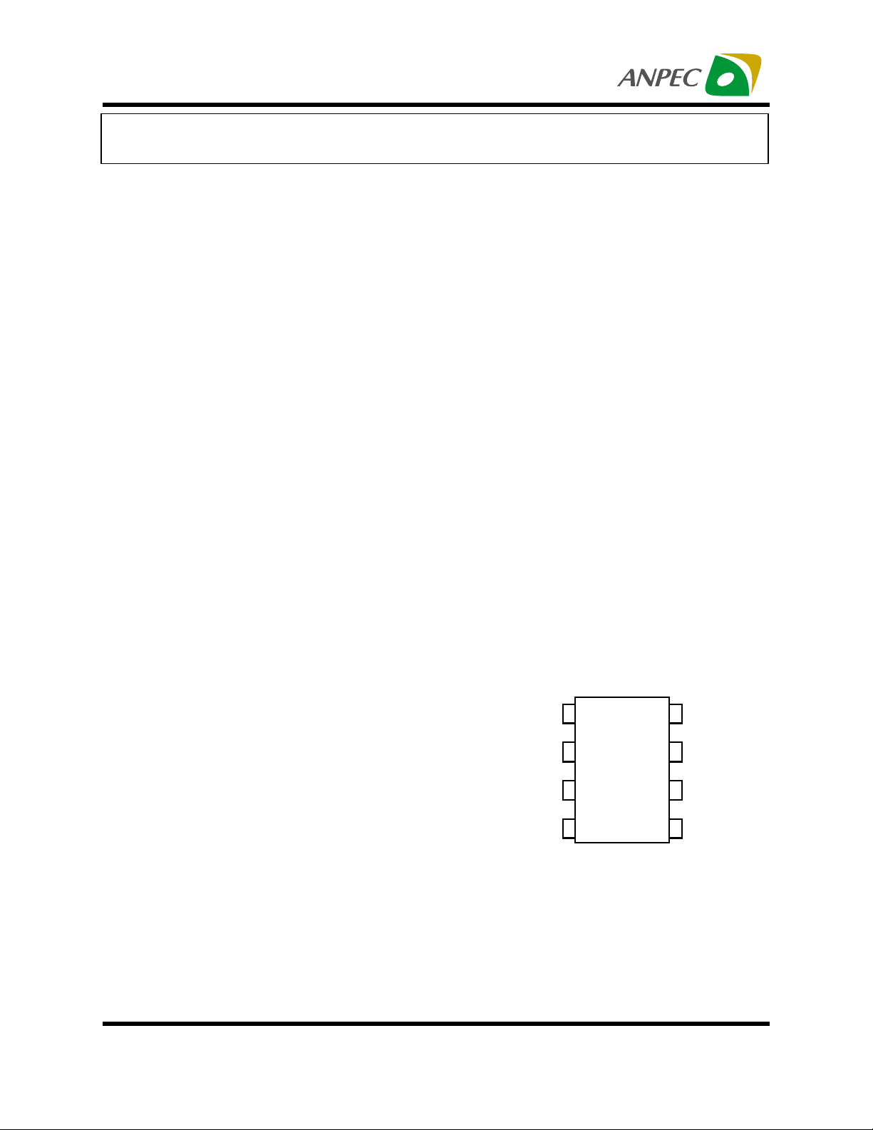
Pin Description
18
NC
ADJ/GND
2
APL1541-33
3
IN
V
4
NC
Front View for SO - 8
OUT
V
7
OUT
V
6
OUT
V
5
OUT
V
www.anpec.com.tw1
APL1541
Ordering and Marking Information
APL1541-
APL1541-
APL1541
XXXXX
Lead Free Code
Handling Code
Temp. R ange
Package Code
Voltage Code
XXXXX - Date C od e
Package Code
K : SOP-8
Temp. R ange
C : 0 to 70 C
Handling Code
TU : Tube TR : Tape & Reel
Voltage Code
33: 3.3V Blank : Adjus table Ve rsion
Lead Free Code
L : Lead Free Device Blank : Orginal Device
APL1541- 33 :
°
APL1541
XXXXX33
XXXXX - Date Code
Absolute Maximum Ratings
Symbol Parameter Rating Unit
V
I
T
J
T
STG
T
L
Input Voltage 13.2
Operating Junction Temperature Range
Control Section
Power Transistor
0 to 125
0 to 150
Storage Temperature Range -65 to +150
Lead Temperature (Soldering, 10 second) 260
V
C
°
C
°
C
°
Electrical Characteristics
Symbol Parameter Test Conditions
V
REF
APL1541
Output Voltage
Reference Voltage
V
OUT
APL1541-33
Line Regulation
REG
LINE
APL1541
APL1541-33
Load Regulation
REG
LOAD
APL1541
APL1541-33
Dropout Voltage
V
D
Copyright ANPEC Electronics Corp.
Rev. A.2 - Oct., 2003
10mA≤ I
T
=0~125°C
J
T
=0~125°C,
J
0≤ I
OUT
T
=0~125°C
J
I
10mA, 1.5V≤(V
=
OUT
I
0A, 4.75V≤(V
=
OUT
T
=0~125°C
J
(V
IN -VOUT
1A, 1.4V≤(V
≤
OUT
1A, 4.75V≤V
≤
=3V, 0≤ I
)
VIN=4.75V, 0≤ I
I
=100mA ,T
OUT
I
=500mA ,T
OUT
I
OUT
=1A ,T
=0~125°C
J
IN
IN -VOUT
IN -VOUT
≤
OUT
1A ,(note 1)
≤
OUT
=0~125°C
J
=0~125°C
J
IN -VOUT
12V,
≤
)
≤7.75V, (note 1)
)
1A ,(note 1)
≤9.75V,
)
≤9.75V, (note1)
APL1541
Min. Typ. Max.
Unit
1.225 1.250 1.275 V
3.235 3.300 3.365 V
0.03
1
0.1
1
0.2
6
0.4
10
mV
mV
11.1
1.05
1.1
1.2
1.3
www.anpec.com.tw2
%
%
V
APL1541
Electrical Characteristics Cont.
Symbol Parameter Test Conditions
I
LIMIT
I
∆
Current Limit
Adjust Pin Current
ADJ
Adjust Pin Current
Change
I
ADJ
APL1541
(V
(V
T
1.4V≤(V
)=5V, TJ=25°C
IN -VOUT
=3V, I
)
IN -VOUT
0~125°C, 10mA≤ I
=
J
IN -VOUT
=10mA, TJ=0~125°C
OUT
1A,
≤
OUT
≤9.75V
)
APL1541
Min. Typ. Max.
1
60 120
0.2 5
Unit
A
A
µ
A
µ
APL1541
Minimum Load
Current
I
O
=0~125°C, (V
T
J
)=9.75V, (note 3)
IN -VOUT
1.7 mA
APL1541
PSRR
Note 1: See thermal regulation specifications for changes in output voltage due to heating effects. Load line regulations are measured at a constant junction temperature by low duty cycle pulse testing.
Note 2: Dropout voltage is specified over the full output current range of the device. Dropout voltage is defined as the minimum input/
output differential measured at the specified output current. Test points and limits are also shown on the Dropout Voltage curve.
Note 3: Minimum load current is defined as the minimum output current required to maintain regulation.
Ripple Rejection F
Thermal
T
R
Regulation
Temperature
T
S
Stability
Long -Term
L
S
Stability
RMS Output
V
N
Noise
Thermal
θ
th
Resistance
Quiescent Current
I
q
APL1541-33
=120Hz, V
RIPPLE
(V
IN -VOUT
T
=25°C, 30ms Pulse
J
T
J
=25°C,10Hz≤F≤10kHz,
T
J
(% of V
=3V, TJ=0~125°C
)
=125°C,1000Hrs.
)
OUT
Junction to Case, at Tab
Junction to ambient
T
=0~125°C,
J
12V
V
≤
IN
RIPPLE
=1V
P-P,
60 75
0.01 0.02 %/ W
0.5
0.3 %
0.003 %
15
50
5.5 10
dB
%
C/ W
°
mA
Copyright ANPEC Electronics Corp.
Rev. A.2 - Oct., 2003
www.anpec.com.tw3
APL1541
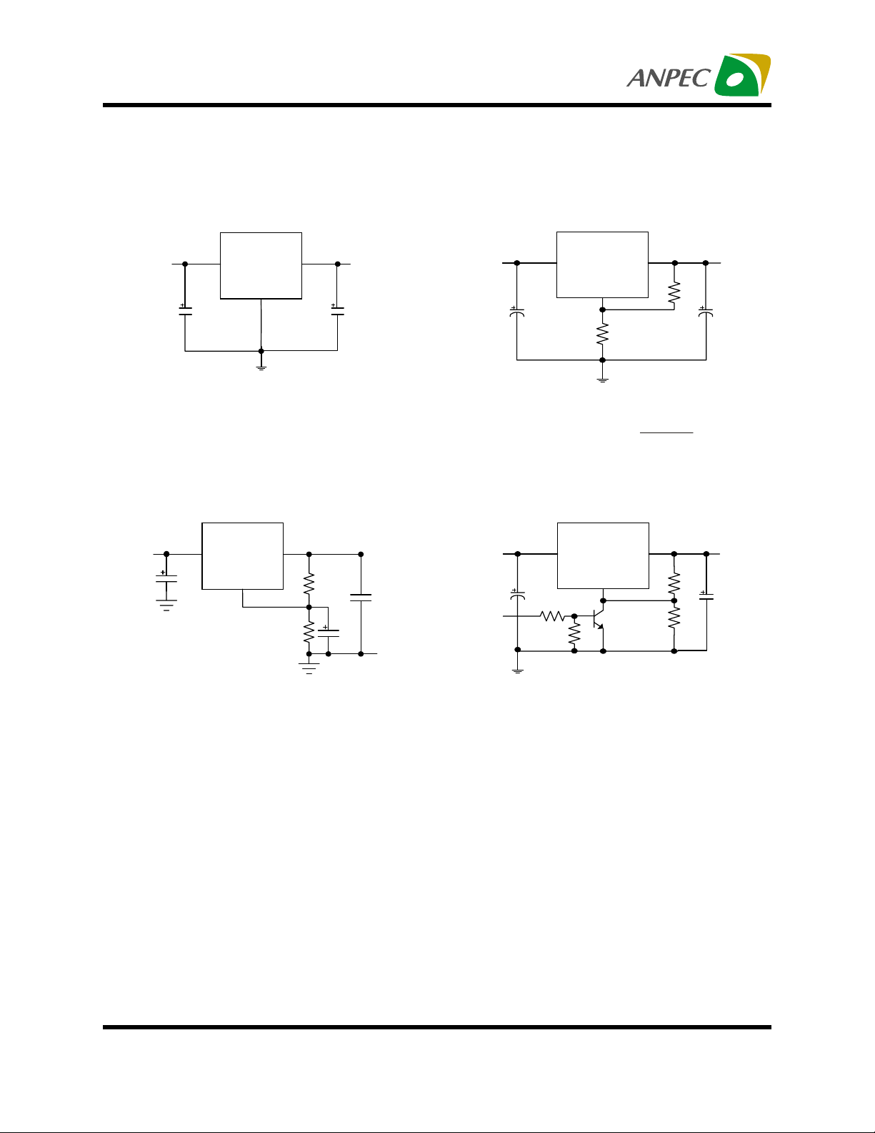
Application Circuits
Simple 5V to 3.3V Regulation
APL15 41-33
IN
=5V
V
10uF
IN
GND
Improving Ripple Rejection
APL15 41
IN
V
10uF
IN
OUT
ADJ
OUT
R2
365
1%
1.25V to 7.75V Adjustable Regulator
APL15 41
IN
V
10uF
OUT
=3.3V
V
10uF
1*
C
IN
ADJ
R2
1K
OUT
121
R1
OUT
V
Ω
100uF
2*
C
*Needed if device is far from filter capacitors
VOUT = 1.250V x
R1+R2
R1
5V Regulator with Shutdown
APL15 41
IN
OUT
V
R1
Ω
121
Ω
C1
10uF
150uF
V
TTL
10uF
1K
IN
1K
ADJ
OUT
121
365Ω
1%
1%
5V
Ω
100uF
*C1 improves ripple rejection.XC should be approximately
equal to R1 at ripple frequency
Copyright ANPEC Electronics Corp.
Rev. A.2 - Oct., 2003
www.anpec.com.tw4
 Loading...