


APA0710/0711
1.1W Mono Low-Voltage Audio Power Amplifier
Features General Description
• Operating Voltage : 2.6V-5.5V
• APA0710 Compatible with TPA711
APA071 1 Compatible with TPA751
• Bridge -Tied Load (BTL) or Single-Ended (SE)
Mode s Operation (for APA0710 only)
• Supply Curren t
– IDD=1.3mA at VDD=5V ,BTL mode
– IDD=0.9mA at VDD=3.3V ,BTL mode
• Low Shutdown Current
– IDD=0.1µA
• Low Distortion
– 630mW, at VDD=5V, BTL, RL=8Ω
THD +N=0.15%
– 280mW, at VDD=3.3V, BTL, RL=8Ω
THD +N=0.15%
• Output Pow er
at 1% TH D+N
– 900mW, at VDD=5V, BTL, RL=8Ω
– 400mW, at VDD=3.3V, BTL, RL=8Ω
at 10% THD+N
–1.1W at VDD=5V, BTL, RL=8Ω
–480mW at VDD=3.3V, BTL, RL=8Ω
The APA0710 is a bridged-tied load (BTL) or singledended (SE) aud io power amplifier developed especially
for low-voltage applications where internal speakers
and external earphone operation are required. The
APA0 711 is a only BTL audio power amplifier developed
especially for low-voltage applications where internal
spea kers are required. Operating with a 5V supply,
the APA0710/1 can deliver 1.1W of continuous power
into a BTL 8Ω load at 10% THD+N througho ut voice
band frequencies. Altho ugh this device is characterized
out to 20kHz,its operatio n is optimized for narrow band
a pplications such as wireless communications. The
BTL conf iguration eliminates the need for external
coup ling capacitors on the output in most applications,
which is particularly important for small battery-powered
equip ment. A unique feature of the APA0710 is that it
allows the a mplifier to switch from BTL to SE on the
fly when an earphone drive is required. This eliminates
complica ted mechanical switching or auxiliary devices
just to drive the external load. This de vice features a
shutd own mode for power-sensitive applications with
sp ecial depop circuitry to eliminate speaker noise when
exiting shutdow n mode. The APA0710/1 are available
in an 8-pin SOP and 8-pin MSOP-P with enhanced
thermal pad.
• Depop Circuitry Integrated
• Thermal Shutdown Protection and
Over Current Protection Circuitry
• High supply voltage ripple rejection
• Surface-Moun t Packaging
– 8 pin MSOP-P (with e nhanced thermal pad)
pow er package available
– SOP-8 package
Applications
• Mobil Phones
• PDAs
• Digital Camera
• Porta ble Electronic Devices
• Lead Free Available (RoHS Compliant)
ANPEC reserves the right to make changes to improve reliability or manufacturability without notice, and advise
customers to obtain the latest version of relevant information to verify before placing orders.
Copyright ANPEC Electronics Corp.
Rev. A.5 - Oct., 2005
www.anpec.com.tw1
APA0710/0711
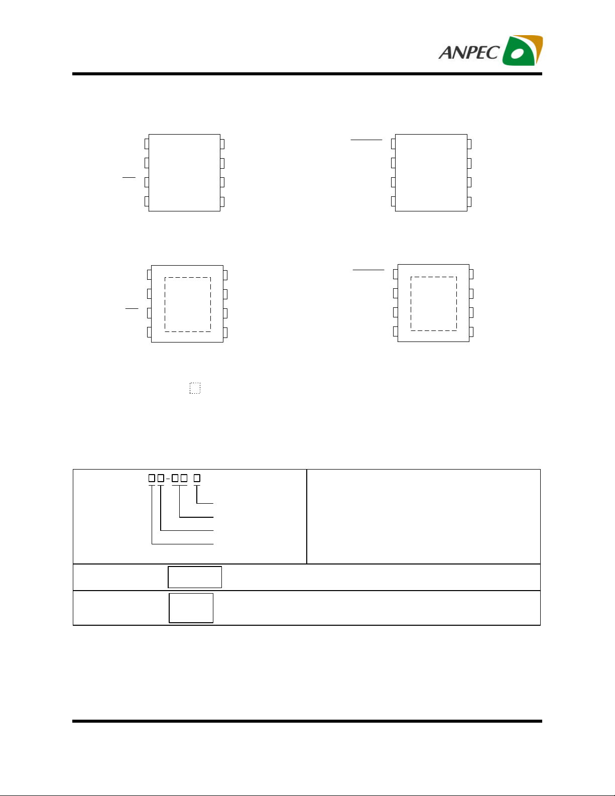
Pin Description
Shutdown
Bypass
SE/BTL
Shutdown
Bypass
SE/BTL
APA0710
1
2
3
4
IN
8
7
6
5
VO-
GND
VDD
VO+
Shutdown
Bypass
IN+
IN-
SOP-8
APA0710
1
2
3
4
IN
8
7
6
5
VO-
GND
VDD
VO+
Shutdown
Bypass
IN+
IN-
MSOP-8-P
1
2
3
4
1
2
3
4
APA0711
SOP-8
APA0711
MSOP-8-P
8
7
6
5
8
7
6
5
VO-
GND
VDD
VO+
VO-
GND
VDD
VO+
NC = N o internal connection
= Th ermal Pad
(con nected to GND plane for better heat dissipation)
Ordering and Marking Information
APA0710/1
Lead Free Code
Handling Code
Temp. Range
Package Code
APA0710/1 K :
APA0710/1 XA :
APA0710/1
XXXXX
A0710/1
XXX
XX
Note: AN PEC lead-free products contain molding compo unds/die attach ma terials and 100% matte tin plate
termination finish; which are fully compliant with RoHS and compatible with both SnPb and lead-free soldiering
op erations. ANPEC lead-free products meet or exceed the lead-free requirements of IPC/JEDEC J STD-020C
fo r MSL classification at lead-free peak reflow temperature.
Copyright ANPEC Electronics Corp.
Rev. A.5 - Oct., 2005
Package Code
K : SOP-8 XA : MSOP-8-P
Temp. Range
I : -40 to 85 C
°
Handling Code
TR : Tape & Reel
Lead Free Code
L : Lead Free Device Blank : Original Device
XXXXX - Date Code
XXXXX - Date Code
www.anpec.com.tw2
APA0710/0711
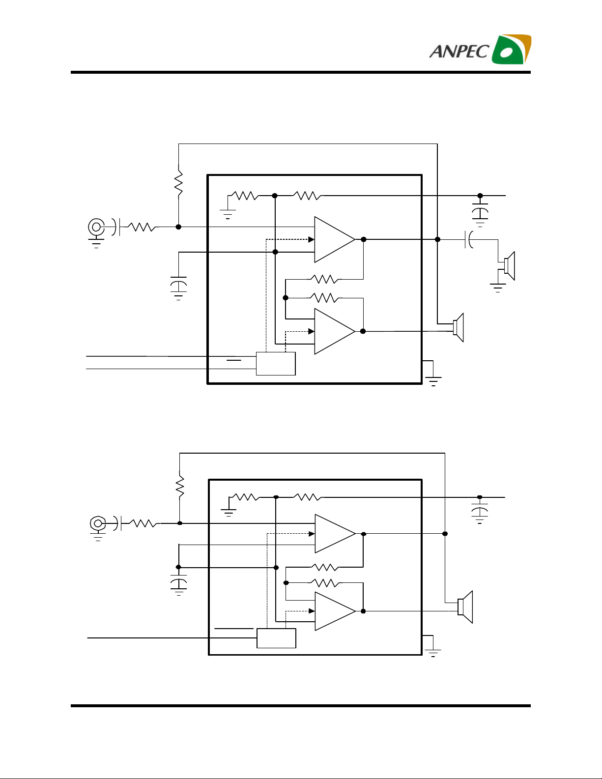
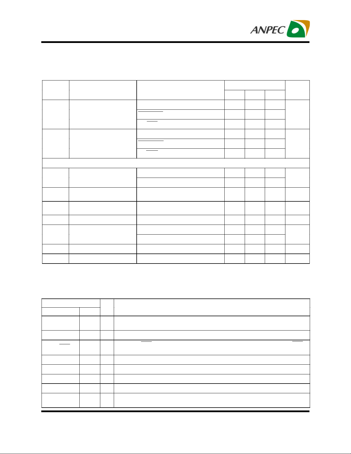
Block Diag ram
Audio
Input
From System Control
From HP Jack
RI
CI
CB
RF
4
IN
Bypass
2
1
Shutdown
3
SE/BTL
VDD/2
Bias
Control
APA0710
VDD
6
VDD
Cs
_
5
Vo+
+
CC
_
Vo-
8
+
7
GND
RF
Audio
Input
From System Control
Copyright ANPEC Electronics Corp.
Rev. A.5 - Oct., 2005
CI
RI
4
3
2
CB
1
IN-
IN+
Bypass
Shutdown
Bias
Control
VDD/2
_
+
_
+
APA0711
VDD
Vo+
Vo-
GND
6
5
8
7
www.anpec.com.tw3
VDD
Cs
APA0710/0711
Absolute Maximum Ratings
(Over operating free-air temperature range un less otherwise noted.)
Symbol Parameter Rating Unit
VDD Supply Voltage -0.3 to 6 V
VIN
TA Operating Ambient Temperature Range -40 to 85
TJ Maximum Junction Temperature Internally Limited*1
T
Storage Temperature Range -65 to +150
STG
TS Soldering Temperature, 10 seconds 260
V
Electrostatic Discharge -2000 to 2000*2 V
ESD
PD Power Dissipation Internally Limited W
Note:
1.APA0710/1 integrated internal thermal shutdown protection when junction temperature ramp up to 170°C
2.Human body model: C=100pF, R=1500Ω, 3 positives pulses plus 3 negative pulses
3.Machine model: C=200pF, L=0.5µF, 3 positive pulses plus 3 negative pulses
Input Voltage Range, Shutdown, SE/BTL
-0.3 to VDD+0.3 V
Recommende d Operating Conditions
Symbol
VDD Supply Voltage
VIH High-Level Voltage
VIL Low-Level Voltage
Parameter Test Conditions Min. Max. Unit
Shutdown, Shutdown
SE/BTL
Shutdown, Shutdown
SE/BTL
2.6 5.5
2.2
0.9VDD
0.4
0.9VDD-1
°C
°
C
°C
°C
V
V
V
Thermal Characteristics
Symbol Parameter Value Unit
R
Thermal Resistance from Junction to Ambient in Free Air
THJA
MSOP-8-P*
SOP-8
* 3.42 in2 printed c ircuit board with 20z trace and copper through 6 vias of 12mil diameter vias.
Th e thermal pad on the MSOP-8-P package with solder on the printed circuit board.
Copyright ANPEC Electronics Corp.
Rev. A.5 - Oct., 2005
50
160
°
C/W
www.anpec.com.tw4
APA0710/0711
Electrical Characteristics
Electrical Characteristics at Spe cified Free - Air Temperature
V
= 3.3V, TA = 25 °C (unless otherwise noted)
DD
Symbol
Parameter Test Conditions
APA0710/1
Min. Typ. Max.
VOO Output Offset Voltage
IDD Supply Current
I
DD(SD)
Supply Current,
Shutdown Mode
RL = 8Ω, RF = 10kΩ
BTL mode, RF = 10kΩ
SE mode, RF = 10kΩ
RF = 10kΩ
20 mV
0.9 1.8
0.55 1.1
0.1 2
Shutdown, VI = VDD 1
Shutdown, VI = VDD 1 |IH|
SE/BTL, VI = VDD
1
Shutdown, VI = 0V 1
Shutdown, VI = 0V 1 |IL|
SE/BTL, VI = 0V 1
Operating characteristic, V
PO Output Power
THD+N
Bom
Total Harmonic Distortion
Plus Noise
Maximum Output Power
Bandwidth
(Note 1)
(Note 1)
= 3.3V, TA = 25°C, RL = 8Ω
DD
THD = 1%, BTL mode, RL = 8Ω
THD = 1%, SE mode, RL = 32Ω
PO = 280mW, BTL mode, RL = 8Ω
Gain = 2, THD+N = 2% 20 kHz
400
40
0.15
B1 Unity-Gain Bandwidth Open Loop 2 MHz
PSRR
Power Supply Rejection
(Note1)
Ratio
Vn Noise Output Voltage
TWU Wake-up time
CB = 1µF, BTL mode, RL = 8Ω
CB = 1µF, SE mode, RL = 8Ω
Gain = 1, CB = 0.1µF
CB = 1µF
74
61
28
380 ms
VDD= 5V, TA= 25 °C (unless otherwise noted)
Unit
mA
µA
µA
µA
mW
%
dB
µV(rms)
Symbol
Parameter Test Conditions
Unit
Min. Typ. Max.
APA0710/1
VOO Output Offset Voltage
IDD Supply Current
I
DD(SD)
Supply Current ,
Shutdown Mode
RL = 8Ω, RF = 10kΩ
BTL mode, RF = 10kΩ
SE mode, RF = 10kΩ
RF = 10kΩ
20 mV
1.3 2.6
mA
0.75 1.5
0.1 2 µ
A
Copyright ANPEC Electronics Corp.
Rev. A.5 - Oct., 2005
www.anpec.com.tw5
APA0710/0711
Shutdown mode control signal input, place entire IC in shutdown mode
When SE/BTL is held low, the APA0710 is in BTL mode. When SE/BTL is
ut in SE
Ele ctrical Characteristics(Cont.)
Electrical Chara cteristics at Specified Free - Air Temperature (Cont.)
VDD= 5V, TA= 25°C (unless otherwise noted)
Symbol
Parameter Test Conditions
Min. Typ. Max.
Shutdown, VI = VDD 1
Shutdown, VI = VDD 1 |IH|
SE/BTL, VI = VDD 1
Shutdown, VI = 0V 1
APA0710/1
|IL|
Shutdown, VI = 0V 1
SE/BTL, VI = 0V 1
Operating characteristic, V
PO
THD+N
Bom
Output Power
Total Harmonic Distortion
Plus Noise
(Note 1)
Maximum Output Power
Bandwidth
= 5V, TA = 25°C, RL = 8Ω
DD
(Note 1)
THD = 1%, BTL mode, RL = 8Ω
THD = 1%, SE mode, RL = 32Ω
PO = 630mW, BTL mode,
RL = 8Ω
Gain = 2, THD+N = 2% 20 kHz
900
94
0.15
B1 Unity-Gain Bandwidth Open Loop 2 MHz
PSRR
Power Supply Rejection
(Note1)
Ratio
Vn Noise Output Voltage
Twu Wake-up time
CB = 1µF, BTL mode, RL = 8Ω
CB = 1µF, SE mode, RL = 8Ω
Gain = 1, CB = 0.1µF
CB = 1µF
74
61
28
400 ms
Unit
µ
µ
mW
%
dB
µ
V(rms)
A
A
Note1 : Output po wer is measured at the output terminals of device at f=1KHz.
Pin Description
APA0710
Pin
Name No
Shutdown 1 I
Bypass 2 I Bypass pin
SE/BTL 3 I
IN 4 I In is the audio input terminal
VO+ 5 O VO+ is the positive output for BTL and SE modes
VDD 6 Supply voltage input pin
GND 7 Ground connection for circuitry
VO- 8
Copyright ANPEC Electronics Corp.
Rev. A.5 - Oct., 2005
I/O
Description
when held high.
held high, the APA0710 is in SE mode
VO- is the negative output in BTL mode and a high-impedance outp
O
mode
www.anpec.com.tw6
APA0710/0711
Shutdown mode control signal input, place entire IC in shutdown mode
Pin Description
APA0711
Pin
Name No
Shutdown 1
I/O
I
when held low.
Description
Bypass 2 I Bypass pin
IN+ 3 I IN+ is the non-inverting input. IN+ is typically tied to the Bypass terminal.
IN- 4 I IN- is the inverting input. IN- is typically used as the audio input terminal.
VO+ 5 O VO+ is the positive BTL output.
VDD 6 Supply voltage input pin.
GND 7 Ground connection for circuitry.
VO- 8 O VO- is the negative BTL output.
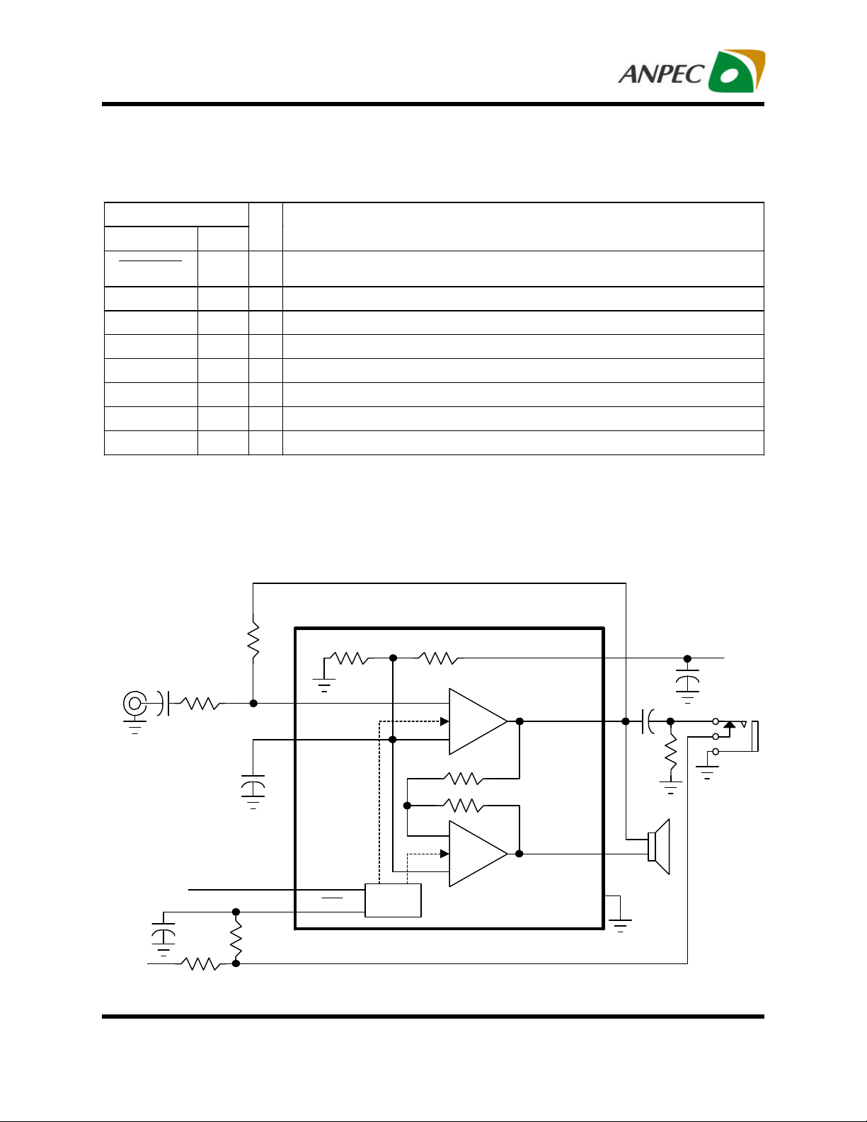
Typ ical Application Circuit
for APA0710 Application
RF
Audio
Input
CI
0.47µ F
RI
10kΩ
10kΩ
CB
1 µF
4
2
IN
Bypass
VDD/2
_
+
VDD
Vo+
6
CC
330µ F
5
1k Ω
VDD
Cs
1µF
_
1
From System Control
0.1µF
VDD
Copyright ANPEC Electronics Corp.
Rev. A.5 - Oct., 2005
100kΩ
100kΩ
Shutdown
SE/BTL
3
Bias
Control
+
Vo-
GND
8
7
www.anpec.com.tw7
APA0710/0711
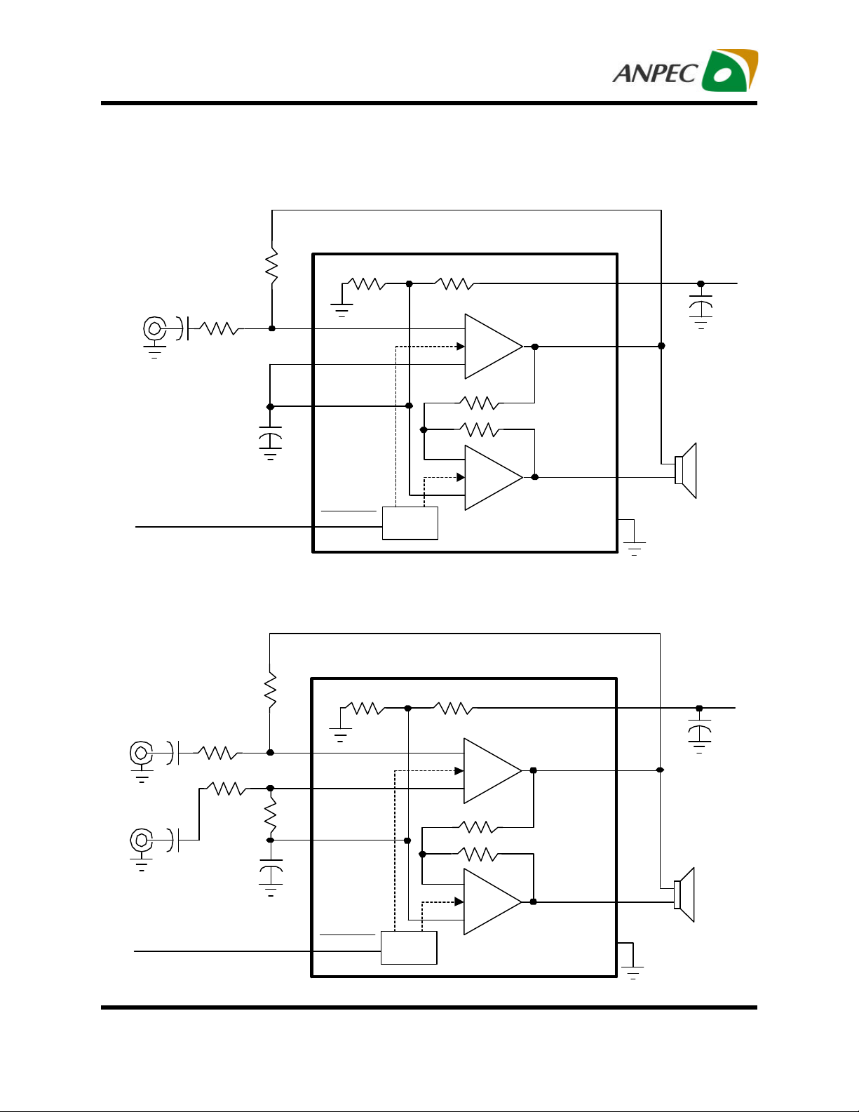
Typ ical Application Circuit (Cont.)
for APA0711 Application
RF
10 kΩ
Audio
Input
0.47µF
CI
RI
10kΩ
CB
1 µ F
4
3
2
IN-
IN+
Bypass
_
+
_
VDD
Vo+
Vo-
6
5
8
VDD
CsVDD/2
1 µ F
From System Control
1
Shutdown
for APA0711 Differential Input Application
RF
10 kΩ
Audio
Input-
Audio
Input+
CI
0.47µF
CI
0.47µF
RI
10kΩ
RI
10kΩ
RF
10 kΩ
CB
1 µ F
4
3
2
IN-
IN+
Bypass
Bias
Control
+
7
GND
VDD
6
_
Vo+
5
VDD
CsVDD/2
1 µ F
+
_
Vo-
8
From System Control
Copyright ANPEC Electronics Corp.
Rev. A.5 - Oct., 2005
1
Shutdown
Bias
Control
+
7
GND
www.anpec.com.tw8
APA0710/0711
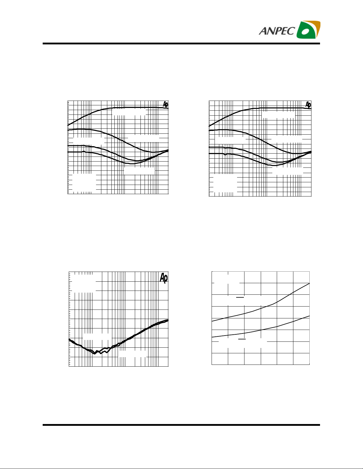
Typ ical Characteristics
PSRR vs. Freque ncy PSRR vs. Freque ncy
+0
No-Capa citor
-20
+0
No-Capa citor
-20
-40
-60
-80
Ripple Rejection Ration (dB)
-100
CB=1 µF
VDD=3.3V
RL=8Ω
SE
Frequency (H z) Frequency (H z)
PSRR vs. Freque ncy
+0
T
RL=8Ω
CB=1 µF
BTL
-20
-40
-60
VDD=3.3V
-80
Ripple Rejection Ration (dB)
-100
20 20k100 1k 10k
VDD=5V
Frequency (H z)
CB=0.1µF
CB=2.2µF
-40
-60
-80
Ripple Rejection Ration (dB)
20k10k1k10020
-100
CB=1 µF
VDD=5V
RL=8Ω
SE
CB=0.1µF
CB=2.2µF
20k10k1k10020
Supply Current vs. Supply Voltage
1600
RF=10kΩ
1400
1200
BTL(SE/BTL=0.1VDD)
1000
800
600
400
Supply Current (µA)
SE(SE/BTL=0.9VDD)
200
0
2.5 3 3.5 4 4.5 5 5.5
Supply Voltage(V)
Copyright ANPEC Electronics Corp.
Rev. A.5 - Oct., 2005
www.anpec.com.tw9

APA0710/0711
Typ ical Characteristics (Cont.)
Supply Current vs. Supply Voltage
0.12
RF=10kΩ
0.11
0.1
0.09
Supply Current (uA)
0.08
2.5 3 3.5 4 4.5 5 5.5
Supply Voltage(V)
Output Pow er vs. Supply Voltage
400
THD+N=1%
350
f=1kHz
SE
300
250
200
150
100
Output Power (mW)
50
0
2.5 3 3.5 4 4.5 5 5.5
RL=8Ω
RL=32Ω
Supply Voltage(V)
Output Pow er vs. Supply Voltage
1200
THD+N=1%
f=1kHz
1000
BTL
800
600
400
RL=8Ω
Output Power (mW)
200
0
2.5 3 3.5 4 4.5 5 5.5
RL=32Ω
Supply Voltage(V)
Output Power vs. Load Resistance
1000
900
800
700
600
500
400
300
200
Output Power (mW)
VDD=3.3V
100
0
8 16 24 32 40 48 56 64
VDD=5V
THD+N=1%
f=1kHz
BTL
Load Resistance(Ω)
Copyright ANPEC Electronics Corp.
Rev. A.5 - Oct., 2005
www.anpec.com.tw10

APA0710/0711
Typ ical Characteristics (Cont.)
Output Power vs. Load Resistance
350
THD+N=1%
f=1kHz
300
SE
250
200
150
100
Output Power (mW)
50
VDD=3.3V
0
8 16 24 32 40 48 56 64
VDD=5V
Load Resistance(Ω)
THD+N vs. Frequen cy
10
VDD=3.3V
RL=8Ω
AV=-2V/V
BTL
THD+N vs. Frequen cy
10
VDD=3.3V
Po=2 50mW
RL=8 Ω
BTL
1
0.1
THD+N (%)
0.01
20 20k
AV=-10V/V
100 1k
AV=-20V/V
Frequency (H z)
THD+N vs. Output Pow er
10
VDD=3.3V
f=1kHz
AV=-2V/V
BTL
AV=-2V/V
10k
1
Po=125mW
0.1
THD+N (%)
0.01
20
100
1k 10k
Frequency (H z)
Copyright ANPEC Electronics Corp.
Rev. A.5 - Oct., 2005
Po=50mW
Po=250mW
20k
1
0.1
THD+N (%)
0.01
0
RL=8Ω
0.1 0.2 0.3
Output Pow er (W)
0.4 0.5
www.anpec.com.tw11
0.6

APA0710/0711
Typ ical Characteristics (Cont.)
10
f=10kHz
1
0.1
THD+N (%)
0.01
0.01
10
RR
VDD=5V
RL=8Ω
AV=-2V/V
BTL
THD+N vs. Output Pow er
f=20kHz
f=1kHz
f=20Hz
VDD=3.3V
RL=8Ω
CB=1µF
AV=-2V/V
BTL
Output Pow er (W)
THD+N vs. Frequen cy
THD+N vs. Frequen cy
10
VDD=5V
Po=700mW
RL=8Ω
BTL
1
AV=-10V/V
0.1
THD+N (%)
0.01
10.1
20 20k100 1k 10k
AV=-20V/V
AV=-2V/V
Frequency (H z)
THD+N vs. Output Pow er
10
VDD=5V
f=1kHz
AV=-2V/V
BTL
1
Po=700mW
0.1
THD+N (%)
0.01
20 20k100
1k
Frequency (H z)
Copyright ANPEC Electronics Corp.
Rev. A.5 - Oct., 2005
Po=50mW
Po=350mW
10k
1
0.1
THD+N (%)
0.01
0.1 0.3
RL=8Ω
0.5
0.7 0.9 1.1 1.2
Output Pow er (W)
www.anpec.com.tw12

APA0710/0711
Typ ical Characteristics (Cont.)
THD+N vs. Output Pow er
10
VDD=5V
RL=8 Ω
CB=1 µF
AV=2V/V
BTL
f=10kHz
f=20kHz
f=1kHz
f=20Hz
0.1
1
0.1
THD+N (%)
0.01
0.01 1
Output Pow er (W)
THD+N vs. Frequen cy
10
R
VDD=3.3V
RL=32Ω
AV=-1V/V
SE
1
THD+N vs. Frequen cy
10
VDD=3.3V
Po=30mW
RL=32Ω
SE
0.1
1
AV=-5V/V
AV=-10V/V
THD+N (%)
AV=-1V/V
0.001
20 100 1k 10k 20k
Frequency (H z)
THD+N vs. Output Pow er
10
VDD=3.3V
f=1kHz
RL=32Ω
AV=-1V/V
SE
1
0.1
Po=15mW
THD+N (%)
0.01
0.001
20 20k100 1k 10k
Frequency (H z)
Copyright ANPEC Electronics Corp.
Rev. A.5 - Oct., 2005
Po=10mW
Po=30mW
0.1
THD+N (%)
0.01
0.001
0.02 0.050.025 0.03 0.035 0.04 0.045
Output Pow er (W)
www.anpec.com.tw13

APA0710/0711
Typ ical Characteristics (Cont.)
10
VDD=3.3V
RL=32Ω
AV=-1V/V
SE
1
0.1
THD+N (%)
0.01
0.001
0.002
10
RRRRR
VDD=5V
RL=32Ω
AV=-1V/V
SE
1
THD+N vs. Output Pow er
f=20Hz
f=20kHz
f=1kHz
0.01
Output Pow er (W)
THD+N vs. Frequen cy
f=10kHz
0.1
10
T T TT T TT TT TTT TT T T TTTTTTTTTTTTTTTTTTTTTTTTTTTTT T
VDD=5V
Po= 60mW
RL=32Ω
SE
1
0.1
THD+N (%)
0.01
0.001
20 20k100
10
VDD=5V
f=1kHz
RL=32Ω
AV=-1V/V
SE
1
THD+N vs. Frequen cy
AV=-10V/V
AV=-5V/V
AV=-1V/V
1k
Frequency (H z)
THD+N vs. Output Pow er
10k
0.1
Po=15mW
Po=30mW
THD+N (%)
0.01
0.001
20 20k
100
Po=60mW
1k
Frequency (H z)
Copyright ANPEC Electronics Corp.
Rev. A.5 - Oct., 2005
10k
0.1
THD+N (%)
0.01
0.02
0.04 0.06 0.08 0.1 0.12
Output Pow er (W)
www.anpec.com.tw14
0.14

APA0710/0711
Typ ical Characteristics (Cont.)
10
VDD=5V
RL=32Ω
AV=-1V/V
SE
1
0.1
THD+N (%)
0.01
0.002 0.20.01
10
VDD=3.3V
RL=10kΩ
AV=-1V/V
SE
1
THD+N vs. Output Pow er
f=20kHz
f=20Hz
f=10kHz
f=1kHz
Output Pow er (W)
THD+N vs. Frequen cy
THD+N vs. Frequen cy
10
1
0.1
VDD=3.3V
Po=0.1mW
RL=10kΩ
SE
AV=-2V/V
AV=-1V/V
T
THD+N (%)
0.01
AV=-5V/V
0.1
20
100
1k
10k
20k
Frequency (H z)
THD+N vs. Output Pow er
10
VDD=3.3V
f=1kHz
RL=10kΩ
AV=-1V/V
SE
1
0.1
THD+N (%)
0.01
20 20k100 1k 10k
Po=0.1mW
Po=0.05mW
Po=0.13mW
Frequency (H z)
Copyright ANPEC Electronics Corp.
Rev. A.5 - Oct., 2005
THD+N (%)
0.1
0.01
50 20075 100 125 150 175
Output Power (µW)
www.anpec.com.tw15

APA0710/0711
Typ ical Characteristics (Cont.)
THD+N vs. Output Pow er
10
VDD=3.3V
RL=10kΩ
AV=-1V/V
SE
1
f=20Hz
0.1
f=20kHz
THD+N (%)
0.01
f=1kHz
50 500
100
f=10kHz
200
Output Power (µW)
THD+N vs. Frequen cy
10
VDD=5V
RL=10kΩ
AV=-1V/V
SE
1
300
400
THD+N vs. Frequen cy
10
1
0.1
TTTTT
VDD=5V
Po=0.3mW
RL=10kΩ
SE
AV=-5V/V
THD+N (%)
0.01
AV=-2V/V
0.001
20 20k
100
1k 10k
Frequency (H z)
THD+N vs. Output Pow er
10
VDD=5V
f=1kHz
RL=10kΩ
AV=-1V/V
1
SE
AV=-1V/V
0.1
THD+N (%)
Po=0.1mW
0.01
Po=0.3mW
0.001
20 20k100 1k 10k
Frequency (H z)
Copyright ANPEC Electronics Corp.
Rev. A.5 - Oct., 2005
Po=0.2mW
0.1
THD+N (%)
0.01
0.001
50
100 150 200 250 300 350 400 450
500
Outpu t Power (µW)
www.anpec.com.tw16

APA0710/0711
Typ ical Characteristics (Cont.)
THD+N vs. Output Pow er
10
VDD=5V
RL=10kΩ
AV=-1V/V
SE
1
f=20Hz
0.1
f=20kHz
THD+N (%)
0.01
f=10kHz
f=1kHz
0.001
10
Output Power (µW)
Close Lo op Gain and Phase vs. Frequency
Close Lo op Gain and Phase vs. Frequency
+28
+24
+20
+16
+12
Phase
Gain
+8
Close Loop Gain (dB)
+4
-0
500100
10 100k100 1k 10k
VDD=3.3V
RL=8Ω
AV=-4V/V
Po=250mW
BTL
+220
+180
+140
+100
Phase(°)
+60
+20
Frequency (H z)
Close Lo op Gain and Phase vs. Frequency
+28
+24
+20
+16
+12
Phase
Gain
+8
Close Loop Gain (dB)
+4
-0
10 100k100
1k
10k
Frequency (H z)
Copyright ANPEC Electronics Corp.
Rev. A.5 - Oct., 2005
VDD=5V
RL=8Ω
AV=-4V/V
Po=700mW
BTL
+220
+180
+140
+100
+60
+20
+10
+8
+6
+4
+2
+0
Phase(°)
-2
-4
-6
Close Loop Gain (dB)
-8
-10
10 100k
100
1k 10k
Frequency (H z)
Gain
Phase
VDD=3.3V
RL=32Ω
AV=-2V/V
Po=30mW
SE
www.anpec.com.tw17
+300
+260
+220
+180
+140
+100
+60
+20
Phase(°)

APA0710/0711
Typ ical Characteristics (Cont.)
Close Lo op Gain and Phase vs. Frequency
+10
+8
+6
+4
+2
+0
-2
-4
Close Loop Gain (dB)
-6
-8
-10
10
100 1k
Gain
Phase
VDD=5V
RL=32Ω
AV=-2V/V
Po=60mW
SE
10k
Frequency (H z)
Noise Floor vs. Frequency
100
100k
+300
+260
+220
+180
+140
+100
+60
+20
Noise Floor vs. Frequency
100
RL= 8Ω, BTL
10
RL= 3 2Ω, SE
Phase(°)
Noise Floor (µVrms)
VDD=3.3V
BW=22Hz to 22kHz
AV=-1V/V
1
20 20k
100 1k
10k
Frequency (H z)
Power D issipation vs. Output Power
350
RL= 8Ω, BTL
10
RL= 3 2Ω, SE
Noise Floor (µVrms)
VDD=5V
BW=22Hz to 22kHz
AV=-1V/V
1
20 20k100 1k 10k
Frequency (H z)
Copyright ANPEC Electronics Corp.
Rev. A.5 - Oct., 2005
300
250
200
150
100
Power Dissipation (mW)
50
0
0 200 400 600
RL=8 Ω
RL=32Ω
Outp ut Power (mW)
www.anpec.com.tw18
VDD=3.3V
BTL

APA0710/0711
Typ ical Characteristics (Cont.)
Power D issipation vs. Output Power
100
90
80
70
60
50
40
30
20
Power Dissipation (mW)
10
0
0 50 100 150
RL=8 Ω
RL=32Ω
Outp ut Power (mW)
Power D issipation vs. Output Power
200
180
160
140
120
100
80
60
40
Power Dissipation (mW)
20
0
0 50 100 150 200 250 300
RL=8 Ω
RL=32Ω
VDD=3.3V
SE
VDD=5V
SE
Power D issipation vs. Output Power
800
700
600
500
400
300
200
Power Dissipation (mW)
100
0
0 200 400 600 800 1000
RL=8 Ω
RL=32Ω
Outp ut Power (mW)
VDD=5V
BTL
Outp ut Power (mW)
Copyright ANPEC Electronics Corp.
Rev. A.5 - Oct., 2005
www.anpec.com.tw19

APA0710/0711
Application Descriptions
BTL Operation
Vo+
OP1
RL
Vo-
Vbias
OP2
Fig ure1:
APA07 10/1 power amplifier internal configuration
The power amplifier OP1 gain is setting by external
gain sett ing, while the second amplifier OP2 is
internally fixed in a unity-gain , inverting configuration.
Figure 1 show s that the output of OP1 is connected
to the input to OP2, which results in the output
signals of with both amplifiers with identical in
magnitude, but out o f phase 180°. Consequently, the
differential gain for each channel is 2X (Gain of SE
mode ).
By driving the loa d differentially through outputs Vo+
a nd Vo-, an amplifier configuration commonly referred
to as bridged mod e is established. BTL mode operation
is diffe rent from the classical single-ended SE amplifier
configuration where one side of its load is connected
to ground.
A BTL amplifier design has a few d istinct advantages
over the SE configuration, as it provides differential
drive to the load, thus doubling the output swing for a
spe cified supply voltage.
Four times the output pow er is possible as compared
to a SE a mplifier under the same conditions. A BTL
configuration, such a s the one used in APA0710, also
cre ates a second advantage over SE amplifiers. Since
the diff erential outputs, Vo+, Vo- are biased at half-
supply, no need DC voltage exists across the load.
This eliminates t he need for an output coupling
capacitor which is required in a single supply, SE
con figuration.
Single-Ended Operation
Consider the single-supply SE configuration shown
Application Circuit. A coupling ca pacitor is required to
block the DC offset voltage from reaching the load.
These capacitors can be quite large (approximately
33µF to 1000 µF) so they tend to be expensive, occupy
valuable PCB are a, and have the additional drawback
of limiting low-frequency perfo rmance of the system
(refer to the Output Coupling Capacitor).
The rules described still hold w ith the addition of the
following relationship :
1
80kCbypass
× O
≤
1
C)R(R
×+
<<
1
(1)
CLIFI CR
Output SE/BTL Opera tion (for APA0710 only)
The ability of the APA0710 to ea sily switch between
BTL and SE modes is one of its most important costs
saving features. This feature eliminates the requirement
for an additional headphon e amplifier in applications
where internal speakers are d riven in BTL mode but
exte rnal headphone or speakers must be accommodated.
Internal to the APA0710, two separate amplifiers drive
Vo+ and Vo- (see Figure 2). The SE/BTL input controls
the operation of the follower amplifier that drives Vo-.
• When SE/BTL is he ld low, the OP2 is turn on and
the APA071 0 is in the BTL mode.
• When SE/BTL is held high, the OP2 is in a high
output impedance state, which configures the
APA0710 as SE driver from Vo +. IDD is reduce d by
a pproximately one-half in SE mode.
Control of the SE/BTL input can be a logic-level TTL
Copyright ANPEC Electronics Corp.
Rev. A.5 - Oct., 2005
www.anpec.com.tw20

APA0710/0711
Application Descriptions (Cont.)
Output SE/BTL Opera tion (for APA0710 only)
sou rce or a resistor divider network or the mono head-
phone jack with switch pin as shown in Application
Circuit.
+
vo
1kΩ
VDD
100kΩ
SE/BTL
100kΩ
Control
Pin
Headphone
Jack
Figure 2: SE/BTL input selection by phonejack p lug
In Figure 2, input SE/BTL operates as follows :
When the phon ejack plug is inserted, the 1kΩ resistor
is disconnected and the SE/BTL input is pulled high
an d enables the SE mode.
When this inp ut goes high level, the Vo- amplifier is
shutdown causing the speaker to mute. The Vo+
a mplifier then drives through the output capacitor (CC)
into the headph one jack.
When there is no headphone plugged into the system,
the contact pin of the headphone jack is connected
from the signal pin, t he voltage divider set up by
resist ors 100kΩ and 1kΩ. Resistor 1kΩ then pulls
low the SE/BTL pin, enabling the BTL function.
Input Capacitor, Ci
In t he typical application an input capacitor, Ci, is
required to allow the amplifier to bias the input sign al
to the proper DC level for optimum operation. In this
case, Ci and the minimum input impedance Ri form a
high-pass filter with the corner f requency determined
in the follow equation :
FC(highpass)=
1
2πRiCi
(2)
The value of Ci is importa nt to consider as it directly
affects the low frequency performance of the circuit.
Consider the example where Ri is 100kΩ and t he
specif ication calls for a flat bass response down to
40Hz. Equa tion is reconfigured as follow :
Ci=
1
2πRifC
(3)
Con sider to input resistance variation, the Ci is 0.04µF
so one would likely choose a value in the range of
0.1µF to 1.0µF.
A furthe r consideration for this capacitor is the leakage
path from the input source through the input network
(Ri+Rf, Ci) to the load.
This leakage current crea tes a DC offset voltage at the
input to the amplifier that reduces useful headroom,
especially in high gain applications. For this re ason a
low-leakage tantalum or ceramic capacitor is the best
choice. When polarized capacitors are used, the
positive side of the ca pacitor should face the amplifier
inpu t in most applications as the DC level there is held
at VDD/2, which is likely higher that the source DC
level. Please note that it is important to confirm the
capacitor polarity in the application.
Effe ctive Bypass Capacitor, Cbypass
As other p ower amplifiers, proper supply bypassing is
critical for low noise performance and high power
supply rejection.
The capacitors located on the bypass and power
supply pins should be as close to the device as
possible. The effect of a larger half supply bypass
capacit or will improve PSRR due to increased halfsupply st ability. Typical application employ a 5V
regulat or with 1.0µF and a 0.1µF bypass as supply
filtering. This does n ot eliminate the need for bypassing
the supply nodes of the APA0710/1. The sele ction of
Copyright ANPEC Electronics Corp.
Rev. A.5 - Oct., 2005
www.anpec.com.tw21

APA0710/0711
Application Descriptions (Cont.)
Effe ctive Bypass Capacitor, Cbypass (Cont.)
bypass capacitors, especially Cbypass, is thus
dependent upon desired PSRR requirements, click
a nd pop performance.
To avoid start-up pop noise occurred, the bypass
voltage should rise slower tha n the input bias voltage
and the relationship shown in equation (4) should be
mainta ined.
<<
O80kCbypass1×
1
(4)
IFI C)R(R
×+
The bypass capacitor is fed f rom a 80kΩ resistor
inside th e amplifier. Bypass capacitor, Cbypass, values
of 0.1µF to 2.2µF ceramic or tantalum low-ESR
capacitors are recommended for the best THD and
noise performan ce.
The bypass capacitance also effects to t he start up
time. It is determined in the following equation :
Tstart up = 5 x (Cbypass x 80kΩ)
(5)
Output Coupling Ca pacitor, Cc (for APA0710 only)
In the typical single-supply (SE) configuration on a
APA0710 , an output coupling capacitor (Cc) is required
to block the DC bias at the output of the amplifier thus
preventing DC currents in the load. As with the input
coupling capacitor, the ou tput coupling capacitor and
imped ance of the load form a high-pass filter governed
by equation.
FC(highpass)=
1
2πR LCC
(6)
For example, a 330µF ca pacitor with an 8Ω speaker
would atten uate low frequencies below 60.6Hz. The
main disad vantage, from a performance standpoint, is
the load impedance is typically small, which drives
the low-frequency corner higher degrading the bass
response. Large value s of CC are required to pass low
frequencies into the load.
Power Supply Decoupling, Cs
The APA0710/1 is a high-perfo rmance CMOS audio
amplif ier that requires adequate power supply
decoupling t o ensure the output total harmonic
distortion (THD) is as low as possible. Power supply
decoupling also prevents the oscillations ca using by
long lead length between the amplifier and the speaker.
The optimum decoupling is achieved by using two
different type capacitors that target on different type
of noise on the power supply leads. For higher freq uency
tran sients, spikes, or digital hash on the line, a good
low equivalent-series-resistance (ESR) ceramic
capacitor, typically 0.1µF pla ced as close as possible
to the device VDD lea d works best. For filtering lowerfreque ncy noise signals, a large aluminum electrolytic
capacitor of 10µF or greater placed near the audio
pow er amplifier is recommended.
Optimizing Depop Circuitry
Circuitry has been included in the APA0710/1 to
minimize the a mount of popping noise at power-up
and when coming out of shutdown mode. Popping
occurs whenever a voltage step is applied to the
speaker. In order t o eliminate clicks and pops, all
ca pacitors must be fully discharged before turn-on.
Rapid on/o ff switching of the device or the shutdown
function will cause the click and pop circuitry. The
valu e of Ci will also affect turn-on pops (refer to Effective
Bypass Capacitance). The bypass volt age rise up
shou ld be slower than input bias voltage.
Alt hough the bypass pin current source cannot be
modified, the size of Cbyp ass can be changed to alter
the de vice turn-on time and the amount of clicks and
pops. By incre asing the value of Cbypass, turn-on pop
can be red uced. However, the tradeoff for using a larger
bypass capacitor is to increase the turn-on time for
this d evice. There is a linear relationship between the
Copyright ANPEC Electronics Corp.
Rev. A.5 - Oct., 2005
www.anpec.com.tw22

APA0710/0711
Application Descriptions (Cont.)
Optimizing Depop Circuitry (Cont.)
size o f Cbypass and the turn-on time.
In a SE configuration, the output coupling capacitor,
CC, is of particu lar concern. This capacitor discharges
throu gh the internal 10kΩ resistors. Depending on the
size of CC, the time constant can be relatively large.
In the most ca ses, choosing a small value of Ci in the
rang e of 0.33µF to 1µF, Cbypass being equal to 1µF
should produce a virtually clickless and popless turn-on.
A high gain amplif ier intensifies the problem as the
small delta in voltage is multip lied by the gain. So it is
adva ntageous to use low-gain configurations.
Shutdown Function
In orde r to reduce power consumption while not in use,
the APA0710/1 contains a shutdown function to
externally turn off t he amplifier bias circuitry. This
shutdown feature turns the amplifier off when a logic
high is pla ced on the Shutdown pin for APA0710 and a
logic low on the Shutdown pin for APA0711.
The trigger point between a logic high and logic low
level is typically 0.4VDD. It is best to sw itch between
groun d and the supply voltage VDD to provide maximum
device performance.
By sw itching the Shutdown/Shutdown pin to high level/
low level, the a mplifier enters a low-current state, I
for APA0710/1. APA0710/1 are in shutdown mode. On
norma l operating, APA0710’s Shutdown pin pull to low
level and APA0711’s Shutdow n pin should pull to high
level to keeping the IC out of the shutdown mode. The
Shutdown/Shutdow n pin should be tied to a definite
voltage to avoid unwa nted state changes.
BTL Amplifier Efficiency
An easy-to-use equation to calculate efficiency starts
out a s being equal to the ratio of power from the power
su pply to the power delivered to the load. The following
equations are t he basis for calculating amplifier
efficiency.
Efficiency =
PO
PSUP
Where :
PO = =
VO,RMS =
VO,RMS x VO,RMS
R L
VP
√2
PSUP = VDD x IDD,AVG = VDDx
VPxVP
2RL
2VP
πRL
Efficiency of a BTL configuration :
PO
VPxVP
( ) / (VDD x ) =
=
PSUP
Po (W) Efficiency (%) VP(V) PD (W)
0.125 33.6 1.41 0.26
0.25 47.6 2.00 0.29
0.375 58.3 2.45* 0.28
*High peak voltages c ause the THD to increase.
Table 1. E fficiency Vs Output Power in 3.3V/8Ω BTL
Systems.
Table 1 employs equation10 to calculate e fficiencies
DD
2RL
2VP
πRL
πVP
4VDD
for thre e different output power levels when load is 8Ω.
The efficiency of the amplifier is quite low for lower
powe r levels and rises sharply as power to the load is
increased result ing in a nearly flat internal power
dissipation over the norma l operating range. Note that
the interna l dissipation at full output power is less than
in the half power range. Calculating the efficiency for a
specific syst em is the key to proper power supply
design. For a mono 900mW audio system with 8Ω
loads and a 5V supply, the maximum draw on the
(7)
(8)
(9)
(10)
Copyright ANPEC Electronics Corp.
Rev. A.5 - Oct., 2005
www.anpec.com.tw23

APA0710/0711
Application Descriptions (Cont.)
BTL Amplifier Efficiency (Cont.)
power supply is almost 1.5W.
A final point to re member about linear amplifiers (either
SE or BTL) is how to manipulate the terms in the
eff iciency equation to utmost advantage when
possible. Note that in equation10, VDD is in the
denominator.
This indicates that a s VDD goe s down, efficiency goes
up. In other words, use the efficiency analysis to choose
the corre ct supply voltage and speaker impedance for
the application.
Power Dissipation
Whether the pow er amplifier is operated in BTL or SE
modes, power dissipation is a major concern. In
equat ion11 states the maximum power dissipation
point for a SE mode operating at a given supply
voltage an d driving a specified load.
2
SE mode : PD,MAX= (11)
VDD
2
2π RL
In BTL mode operation, the output voltage swing is
doubled as in SE mode. Thus the maximum power
dissipation point for a BTL mode operating at the same
given conditions is 4 times as in SE mode.
2
BTL mode : PD,MAX=
4VDD
2
2π RL
(12)
Since the APA0710/1 is a mono channel power
a mplifier, the maximum internal power dissipation is
equa l to the both of equations depending on the mode
of operation. Even with this substantial increase in
power dissipation, the APA0710/1 does not require
extra hea tsink. The power dissipation from equation12,
a ssuming a 5V-power supply and an 8Ω load, must
not be greater than the power dissipation that results
from the equation13 :
PD,MAX=
TJ,MAX - TA
θJA
(13)
For MSO P-8-P package with and SOP-8 without
thermal pad, the thermal resistance (θJA) is equal to
50οC/W an d 160οC/W, respe ctively.
Since the maximum junction temperature (T
J,MAX
) of
APA0710/1 are 170οC a nd the ambient temperature
(TA) is defined by the power system design, the
maximum power dissipation wh ich the IC package is
ab le to handle can be obtained from equation13. Once
the power dissipation is greater than the maximum
limit (P
), e ither the supply voltage (VDD) must be
D,MAX
de creased, the load impedance (RL) must be increased
or the a mbient temperature should be reduced.
Thermal Pad Considerations
The thermal pad must be connected to ground. The
pa ckage with thermal pad of the APA0710/1 requires
special attention on thermal design. I f the thermal
design issues are not properly addressed, the
APA0710/1 8Ω will go into thermal shutdown when
driving a 8Ω load.
The thermal pad on the bottom of the APA0710/1
should be soldered down to a copper pad on the
circuit board. He at can be conducted away from the
thermal pad through the copper pla ne to ambient. If
the copper pla ne is not on the top surface of the circuit
board, 6 to 10 vias of 12 mil or smaller in diameter
sho uld be used to thermally couple the thermal pad to
the bottom plane. For good thermal conduction, the
vias must be plated through and solder filled. The
copper plane used t o conduct heat away from the
thermal pad should be as large as practical.
If the a mbient temperature is higher than 25°C, a larger
copper p lane or forced-air cooling will be required to
keep the APA0710/1 junction te mperature below the
therma l shutdown temperature (170°C).
In higher a mbient temperature, higher airflow rate
and/or larger cop per area will be required to keep the
IC out of thermal shu tdown.
Copyright ANPEC Electronics Corp.
Rev. A.5 - Oct., 2005
www.anpec.com.tw24

APA0710/0711
Packa ging Information
SOP-8 pin ( Reference JEDEC Registration MS-012)
HE
0.015X45
e1 e2
D
A1
A
0.004max.
Dim
A 1.35 1.75 0.053 0.069
A1 0.10 0.25 0.004 0.010
D 4.80 5.00 0.189 0.197
E 3.80 4.00 0.150 0.157
H 5.80 6.20 0.228 0.244
L 0.40 1.27 0.016 0.050
e1 0.33 0.51 0.013 0.020
e2 1.27BSC 0.50BSC
φ
1
Min. Max. Min. Max.
Millimeters Inches
0° 8° 0° 8°
1
L
Copyright ANPEC Electronics Corp.
Rev. A.5 - Oct., 2005
www.anpec.com.tw25

APA0710/0711
Packa ging Information
MSOP-8-P
e1
A1
E
Dim
H1
D1
e
A3
Min. Max. Min. Max.
E1
C
0.25
A2
Millimeters Inches
A1 0.06 0.15 0.002 0.006
A2 0.86 TYP 0.34 TYP
A3 0.25 0.4 0.01 0.0126
C 0.13 0.23 0.005 0.009
e 0.65 TYP 0.0256 TYP
e1 2.90 3.1 0.114 0.122
E 4.8 5.0 0.189 0.197
E1 2.90 3.1 0.114 0.122
D1 2.146 REF 0.0845 REF
H1 1.740 REF 0.0685 REF
L 0.9 1.0 0.036 0.039
L1 0.45 0.65 0.018 0.026
φ
6° 6°
GAUGE
PLANE
L
L1
Copyright ANPEC Electronics Corp.
Rev. A.5 - Oct., 2005
www.anpec.com.tw26

APA0710/0711
Physical Specifications
Terminal Material Solder-Plated Copper (Solder Material : 90/10 or 63/37 SnPb), 100%Sn
Lead Solderability Meets EIA Specification RSI86-91, ANSI/J-STD-002 Category 3.
Reflow Condition (IR/Convection or VPR Reflow)
T
P
Ramp-up
T
L
Tsmax
Tsmin
Temperature
ts
Preheat
25
°
t 25 C to Peak
Classificatin Reflow Profiles
tp
Ramp-down
Time
Critical Zone
TL to T
P
t
L
Profile Feature Sn-Pb Eutectic Assembly Pb-Free Assembly
Average ramp-up rate
(TL to TP)
Preheat
-
Temperature Min (Tsmin)
-
Temperature Max (Tsmax)
-
Time (min to max) (ts)
Time maintained above:
-
Temperature (TL)
-
Time (tL)
Peak/Classificatioon Temperature (Tp)
Time within 5°C of actual
Peak Temperature (tp)
Ramp-down Rate
Time 25°C to Peak Temperature
3°C/second max. 3°C/second max.
100°C
150°C
60-120 seconds
183°C
60-150 seconds
150°C
200°C
60-180 seconds
217°C
60-150 seconds
See table 1 See table 2
10-30 seconds 20-40 seconds
6°C/second max. 6°C/second max.
6 minutes max. 8 minutes max.
Notes: All temperatures refer to topside of the package .Measured on the body surface.
Copyright ANPEC Electronics Corp.
Rev. A.5 - Oct., 2005
www.anpec.com.tw27

APA0710/0711
Classifica tin Reflow Profiles(Cont.)
Table 1. SnPb Entectic Process – Package Peak Reflow Temperature s
Package Thickness Volume mm
<350
<2.5 mm
≥
2.5 mm 225 +0/-5°C 225 +0/-5°C
240 +0/-5°C 225 +0/-5°C
3
Volume mm
3
≥ 350
Table 2. Pb-free Process – Package Classification Reflow Temperatures
Package Thickness Volume mm3
<350
<1.6 mm
1.6 mm – 2.5 mm
≥
2.5 mm 250 +0°C* 245 +0°C* 245 +0°C*
260 +0°C* 260 +0°C* 260 +0°C*
260 +0°C* 250 +0°C* 245 +0°C*
*Tolerance: The device manufacturer/supplier
shall
Volume mm3
350-2000
Volume mm3
>2000
assure process compatibility up to and
including the stated classification temperature (this means Peak reflow temperature +0°C.
For example 260°C+0°C) at the rated MSL level.
Reliab ility Test Program
Test item Method Description
SOLDERABILITY MIL-STD-883D-2003
HOLT MIL-STD-883D-1005.7
PCT JESD-22-B,A102
TST MIL-STD-883D-1011.9
ESD MIL-STD-883D-3015.7 VHBM > 2KV, VMM > 200V
Latch-Up JESD 78 10ms, 1tr > 100mA
245°C, 5 SEC
1000 Hrs Bias @125°C
168 Hrs, 100%RH, 121°C
-65°C~150°C, 200 Cycles
Carrier Tape & Reel Dimensions
E
Po
F
W
Copyright ANPEC Electronics Corp.
Rev. A.5 - Oct., 2005
P
P1
Ao
t
D
Bo
Ko
D1
www.anpec.com.tw28

APA0710/0711
12.4 +0.2
Carrie r Tape & Reel Dimensions(Cont.)
J
C
A
T2
B
T1
Application
M/SOP-8
A B C J T1 T2 W P E
330±1 62 ± 1.5
F D D1 Po P1 Ao Bo Ko t
5.5 ± 0.1 1.55±0.1
12.75 +
0.1 5
1.55+ 0.25
2 + 0.5
4.0 ± 0.1 2.0 ± 0.1 6.4 ± 0.1 5.2± 0.1 2.1± 0.1 0.3±0.013
2± 0.2
12 + 0.3
- 0.1
8± 0.1 1.75± 0.1
(mm)
Cover Tape Dimensions
Application Carrier Width Cover Tape Width Devices Per Reel
SOP- 8
MSOP- 8
12 9.3 2500
12 9.3 3000
Customer Service
Anpe c Electronics Corp.
Head Office :
No.6, Dusing 1st Road, SBIP,
Hsin-Chu, Taiwan, R.O.C.
Tel : 886-3-5642000
Fax : 886-3-5642050
Taipei Branch :
7F, No. 13 7, Lane 235, Pac Chiao Rd.,
Hsin Tien City, Taipei Hsien, Taiwan, R. O. C.
Tel : 886-2 -89191368
Fax : 8 86-2-89191369
Copyright ANPEC Electronics Corp.
Rev. A.5 - Oct., 2005
www.anpec.com.tw29

 Loading...