


ANPEC APA4801KI-TR, APA4801JI-TU, APA4801JI-TR Datasheet
APA4801
Stereo 280mW 8Ω Speaker Driver with Mute
Features
••
•
Operating Voltage
••
Single Supply 3V to 7V
Dual Supply ±1.5V to ± 3.5V
••
•
High Signal-to-Noise Ratio 100dB
••
••
•
High Slew Rate 5V/ µs
••
••
•
Low Distortion -65dB
••
••
• Output Power at 10% THD+N
••
into 8Ω 280mW
into 16Ω 160mW
••
• Large Output Voltage Swing
••
••
• Excellent Power Supply Ripple Rejection
••
••
• Flexible Mute Function
••
••
• Integrated Voltage Divider (V
••
nate External Resistors
••
• Low Power Consumption
••
••
• Short-circuit Elimination
••
••
• Wide Temperature Range
••
••
• No Switch ON/OFF Clicks
••
••
• Available in 8 pin SOP or DIP Package
••
/2) to Elimi-
DD
Applications
••
• Portable Digital Audio
••
••
•
Personal Computers
••
••
•
Microphone Preamplifier
••
General Description
The APA4801 is an integrated class AB stereo headphone amplifier contained in an SO-8 or a DIP-8 plastic package with Mute feature . Besides the common
Mute feature , the APA4801 further integrates a voltage divider inside the chip . Thus , the external resistors can be eliminated . The device has been primarily developed for portable digital audio applications .
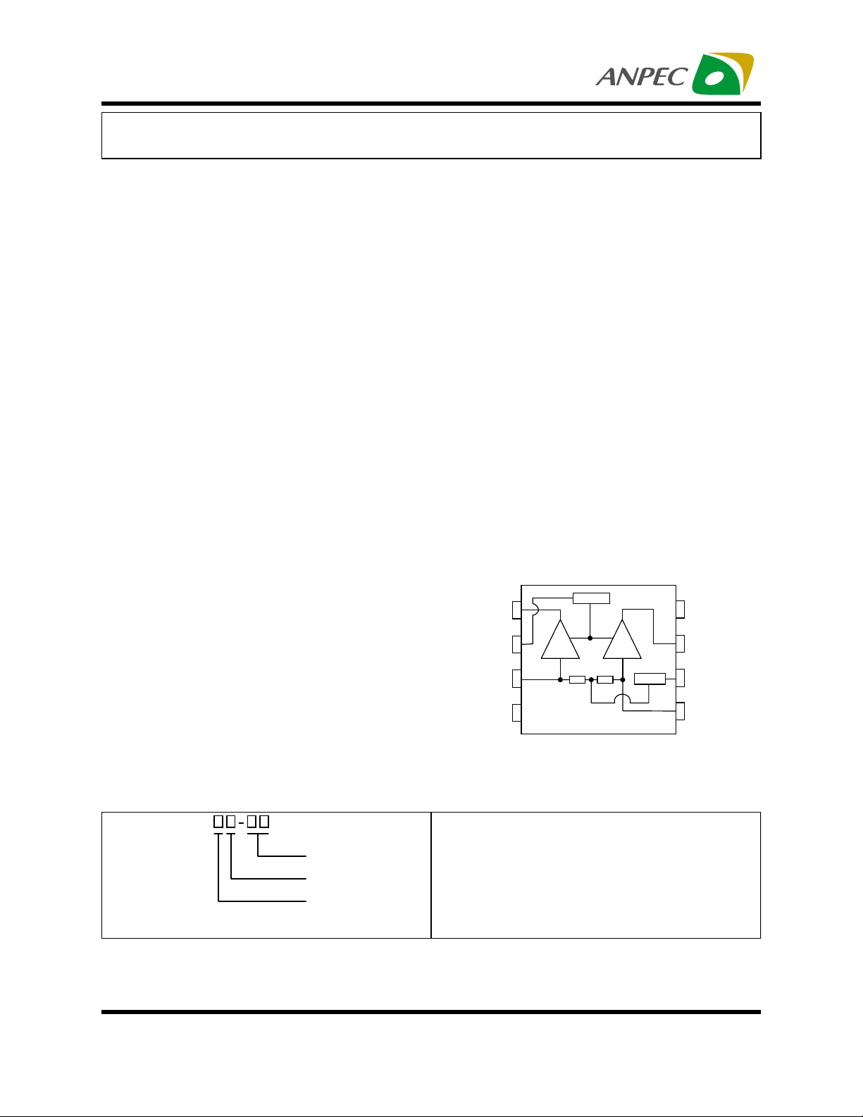
Block Diagram
Out A
Mute
Input A
1
2
3
MUTE
0dB
0dB
A
+
130k
B
+
Ω
Ω
130k
BIAS
8
7
6
V
DD
Out B
BIAS
V
4
SS
5
Input B
Ordering Information
APA4801
Handling Code
Temp. Range
Package Code
ANPEC reserves the right to make changes to improve reliability or manufacturability without notice, and advise
customers to obtain the latest version of relevant information to verify before placing orders.
Copyright ANPEC Electronics Corp.
Rev. A.5 - Apr., 2001
Package Code
J : PDIP-8 K : SOP-8
Temp. Range
I : - 40 to 85 C
Handling Code
TU : Tube
TR : Tape & Reel
°
www.anpec.com.tw1

APA4801
Function Pin Description
Pin Name I/O Function Description
Out A O A channel output pin
Mute I
Input A I A channel input terminal
V
SS
Input B I B channel input terminal
BIAS I Right channel bias input pin
OUT B O B channel output pin
V
DD
Absolute Maximum Ratings
Symbol Parameter Rating Unit
V
DD
t
SC(O)
T
T
T
STG
T
V
ESD
Note: 1. Human body model : C=100pF, R=1500Ω, 3 positive pulses plus 3 negative pulses
Supply Voltage 8 V
Output Short-circuit Duration, at TA=25°C, P
Operating Ambient Temperature range -40 to 85
A
Maximum Junction Temperature 150
J
Storage Temperature Range -65 to +150
Soldering Temperature,10 seconds 260
S
Electrostatic Discharge -3000 to 3000
Chip disable control input, high active and low for normal
operating
Power ground pin
Power input pin
tot
=1W
20 S
*1
C
°
C
°
C
°
C
°
V
Thermal Characteristics
Symbol Parameter Value Unit
R
THJA
Electrical Characteristics V
V
DD
VDD=5V
I
DD
V
I(OS)
Copyright ANPEC Electronics Corp.
Rev. A.5 - Apr., 2001
Thermal Res i stance fr om Jun ction to Ambie n t in Free Air
DIP-8
SO-8
=0dBV, VDD=5V, TA=25°C, f=1kHz (unless otherwise noted)
IN
109
210
APA4801Symbol Parameter Test Conditions
Min. Typ. Max.
Power Supply Voltage 2.7 5.5
Supply Current No Load 2.5 mA
Input Offset Voltage 5 50 mV
www.anpec.com.tw2
K/W
K/W
Unit
V

APA4801
Electrical Characteristics Cont.
APA4801Symbol Parameter Test Conditions
Min. Typ. Max.
I
Shunt Current 200
SD
Mu te l Mu te In pu t Volta ge 0.8 V
AV1- AV2Differential Channel
-0.5 0 0.5 dB
Volt ag e G ain
ATT Mute Attenuation fIN=1k, VIN =1 Vrms 75 70 dB
AC Characteristics
(THD+N
)/S
P
O
To tal Har moni c
Distortion plus Noise to
Signal Ratio
=160mW, RL=8Ω, f=1 kHz
P
O
=100mW, RL=16Ω, f=1 k H z
P
O
Output Power (THD+N)/S =0.1%, f=1kHz,
0.05
0.05
BW<80kHz
RL=8
Ω
RL=16
Ω
P
Output Power (THD+N)/S=10%, f=1kHz,
O
170
100
BW<80kHz
280
160
76 dB
PSRR Power Supply
R ejectio n Ratio
S/N Signal to Noise Ratio
RL=8
Ω
RL=16
Ω
C
=4.7 µF,V
B
=200mVrms,
RIPPLE
f=120Hz
R
=8
Ωµ
L
VDD=3V
I
Supply Current No Load 2.2 mA
DD
V
Input Offset Voltage 5 m V
I(OS )
I
SD
200
AC Characteristics
I
Shunt Current 150
SD
Mu te l Mu te Inp u t Voltag e 0.8 V
AV1- AV2Differential Channel
-0.5 0 0.5 dB
Volt ag e G ain
ATT Mute Attenuation fIN=1k ,VIN = 0.5Vrms 70 dB
(THD+
N)/S
To tal Har moni c
Distortion plus Noise to
Signal Ratio
P
=50mW, RL=8Ω, f=1 k H z
O
=25mW, RL=16Ω, f=1 kHz
P
O
0.1
0.1
S/N Signal to Noise Ratio
P
Output Power (THD+N)/S=0.1%, f=1kHz,
O
BW<80kHz
RL=8
Ω
RL=16
Ω
P
Output Power (THD+N)/S=10%, f=1kHz,
O
45
25
BW<80kHz
80
45
76 dB
PSRR Power Supply
R ejectio n Ratio
RL=8
Ω
RL=16
Ω
=4.7µF,V
C
B
f=120Hz
=200m Vrms,
RIPPLE
Unit
µ
mW
mW
Vrm s
µ
µ
Vrm s
µ
mW
mW
A
%
A
A
%
Copyright ANPEC Electronics Corp.
Rev. A.5 - Apr., 2001
www.anpec.com.tw3
APA4801
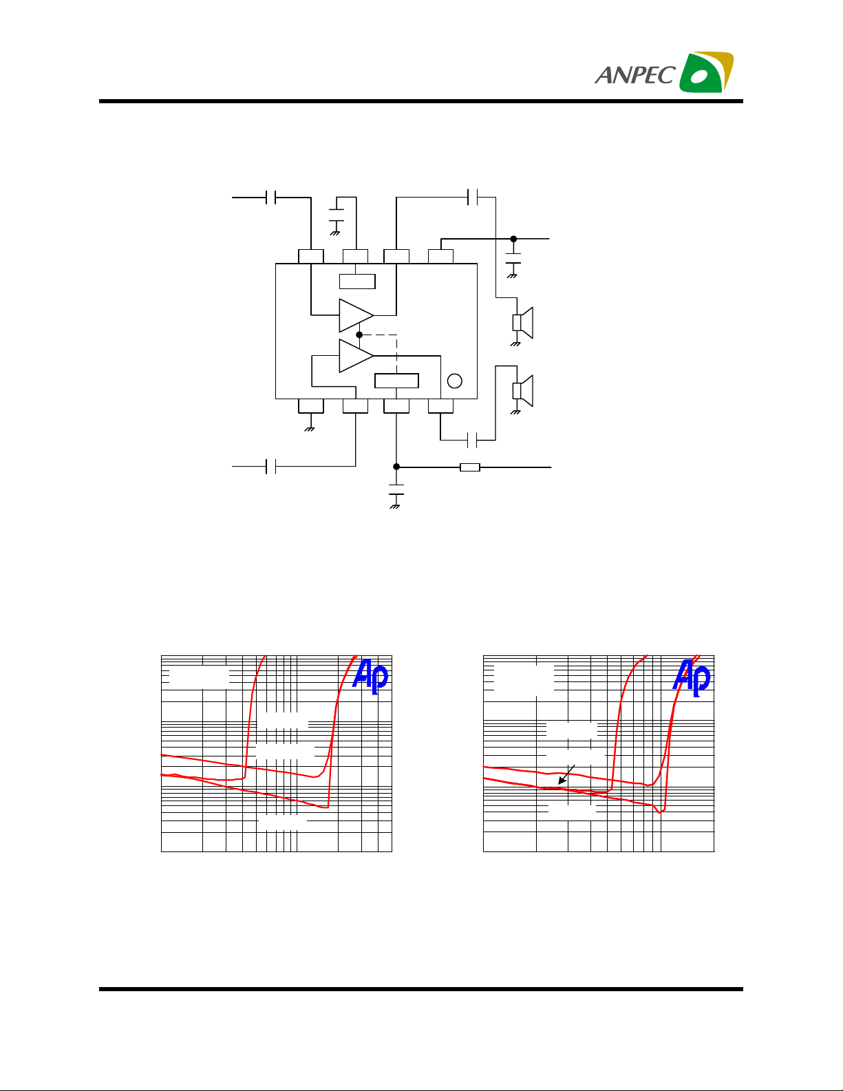
Test and Application Circuit
F
1
µ
V
INB
4.7
F
µ
57
4
V
SS
1µF
V
INA
68
BIAS
0dB
+
B
0dB
+
A
32 1
Input A
Mute
1µF
Out BInput B
BIAS
V
APA4801
MUTE
Out A
220µF
V
100µF
DD
V
MUTE
H : Speaker Action
L : Mute on
DD
220µF
100k
Ω
Typical Characteristics
THD+N vs Output Power
10
VDD= 5V
Ω
=8
R
L
1
THD+N (%)
0.1
0.01
10m 500m
f=20Hz
f=20kHz
f=1kHz
200m
Output Power (W)
THD+N vs Output Power
10
VDD= 5V
Ω
=16
R
L
1
f=20Hz
f=20kHz
THD+N (%)
0.1
f=1kHz
0.01
10m 200m
100m
Output Power (W)
Copyright ANPEC Electronics Corp.
Rev. A.5 - Apr., 2001
www.anpec.com.tw4

APA4801
Typical Characteristics Cont.
THD+N vs Frequency
10
VDD= 5V
=160mW
P
O
Ω
=8
R
L
NO FILTERS
1
THD+N (%)
0.1
0.01
20 20k100 1k 10k
Frequency (Hz)
THD+N vs Frequency
10
VDD= 5V
=100mW
P
O
Ω
=16
R
L
NO FILTERS
1
THD+N (%)
0.1
0.01
20 20k100 1k 10k
Frequency (Hz)
THD+N vs Output Power
10
VDD= 3V
Ω
=8
R
L
1
f=20kHz
THD+N (%)
0.1
0.01
10m 100m50m
f=20Hz
f=1kHz
Output Power (W)
THD+N vs Output Power
10
VDD= 3V
Ω
=16
R
L
1
THD+N (%)
0.1
0.01
10m 100m50m
f=20kHz
f=20Hz
Output Power (W)
f=1kHz
Copyright ANPEC Electronics Corp.
Rev. A.5 - Apr., 2001
www.anpec.com.tw5
 Loading...