


ANPEC APL1085-UC-TU, APL1085-UC-TR, APL1085-GC-TU, APL1085-GC-TR, APL1085-FC-TU Datasheet
...
Copyright ANPEC Electronics Corp.
Rev. B.5 - Jun., 2003
APL1085
www.anpec.com.tw1
ANPEC reserves the right to make changes to improve reliability or manufacturability without notice, and advise
customers to obtain the latest version of relevant information to verify before placing orders.
3A Low Dropout Fast Response Positive Adjustable Regulator and Fixed 3.3V
••
••
• Fast Transient Response
••
••
• Guaranteed Dropout Voltage at Multiple Cur-
rents
••
••
• Load Regulation : 0.05% Typ.
••
••
• Line Regulation : 0.03% Typ.
••
••
• Low Dropout Voltage : 1.2V Typ. at I
OUT
=3A
••
••
• Trimmed Current Limit : 3A Typ. at T
J
=125 °C
••
••
• On-Chip Thermal Limiting : 150 °C Typ.
••
••
• Standard 3-pin TO-220 , TO-252 and TO-263
Power Package
Features General Description
Applications
••
••
• Pentium
TM
Processor Supplies
••
••
• PowerPC
TM
Supplies
••
••
• Low Voltage Logic Supplies
••
••
• Battery-Powered Circuitry
••
••
• Post Regulator for Switching Power Supply
The APL1085 is a low dropout three-terminal adjustable regulator with 3A output current capability. In
order to obtain lower dropout voltage and faster transient response, which is critical for low voltage
applications, the APL1085 has been optimized. The
output available voltage range of adjustable version
is from 1.25~5.75V with an input supply below 7V ,
and the fixed 3.3V output voltage device is also
available.
Current limit is trimmed to ensure specified output
current and controlled short-circuit current. On-chip
thermal limiting provides protection against any combination of overload that would create excessive junction temperatures.
The APL1085 is available in both the through-hole
and surface mount versions of the industry standard
Front View APL1085 TO-263 Package
Front View APL1085 TO-252 Package
1
2
3
V
IN
V
OUT
ADJ
TAB is V
OUT
Front View APL1085 TO-220 Package
Pin Description
TAB is V
OUT
1
2
3
V
IN
V
OUT
ADJ
1
2
3
V
IN
V
OUT
ADJ
TAB is V
OUT
Copyright ANPEC Electronics Corp.
Rev. B.5 - Jun, 2003
APL1085
www.anpec.com.tw2
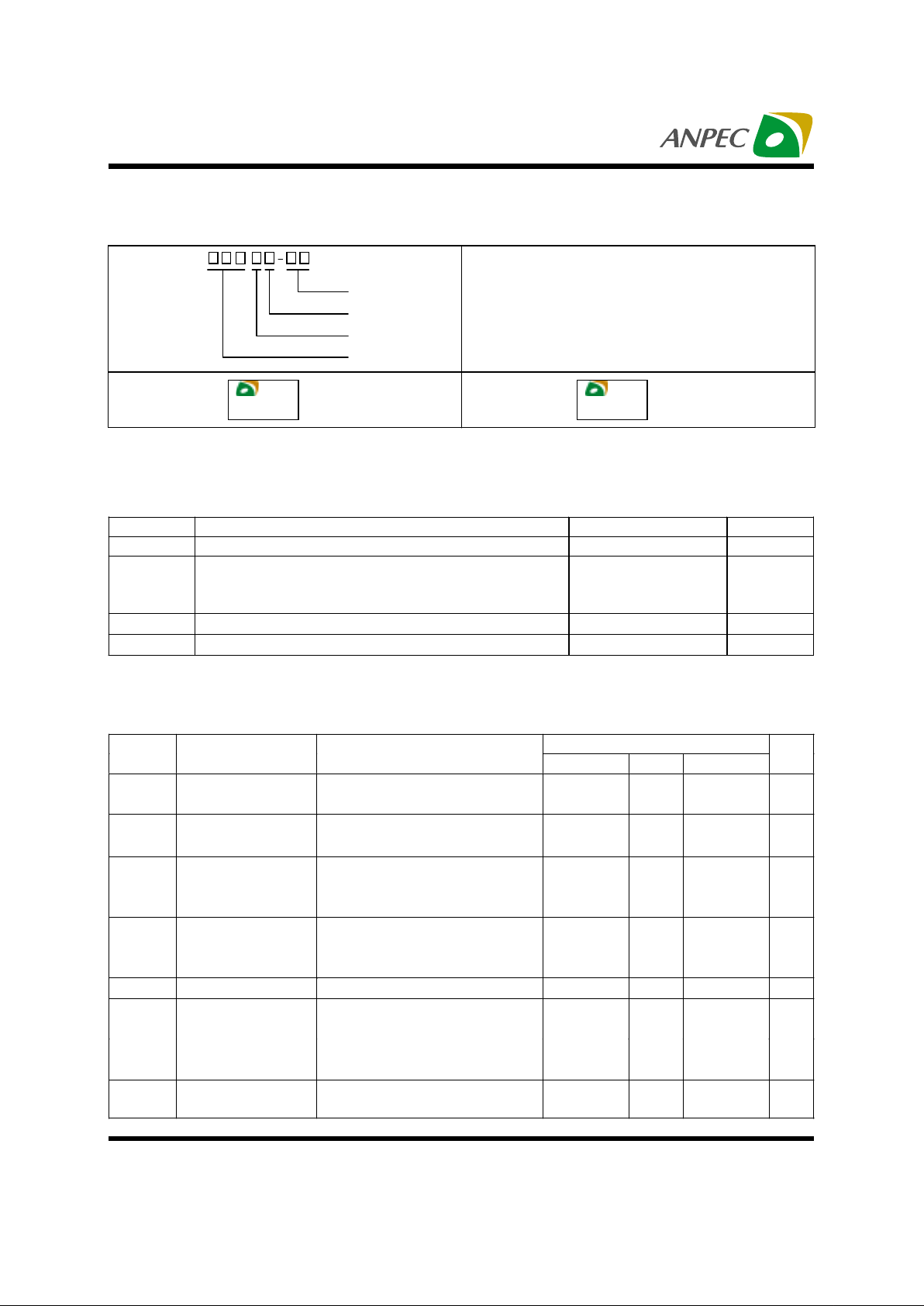
Ordering Information
Package Code
F : TO-220 G : TO-263 U : TO-252
Temp. Range
C : 0 to 70 C
Handling Code
TU : Tube TR : Tape & Reel
Voltage Code :
33 : 3.3V Blank : Adjustable Version
°
APL1085-
Handling Code
Temp. Range
Package Code
Voltage Code
APL1085:
APL1085
XXXXX
- Date Code
XXXXX
APL1085-33 :
APL1085
XXXXX
- Date Code
XXXXX
33
Symbol Parameter Rating Unit
V
I
Input Voltage 7 V
T
J
Operating Junction Temperature Range
Control Section
Power Transistor
0 to 125
0 to 150
°
C
T
STG
Storage Temperature Range -65 to +150
°
C
T
L
Lead Temperature (Soldering, 10 second) 260
°
C
Absolute Maximum Ratings
Electrical Characteristics
APL1085Symbol Parameter Test Conditions
Min. Typ. Max.
Unit
V
REF
Reference Voltage
1.5V≤(V
IN -VOUT
)
≤5.75V,
10mA≤ I
OUT
≤
3A, T
J
=0~125°C
1.225(-2%) 1.250 1.275(+2%) V
V
OUT
Output Voltage
APL1085-3.3
10mA≤ I
OUT
≤
3A, 4.75V≤V
IN
≤
7V,
T
J
=0~125°C
3.235(-2%) 3.300 3.365(+2%) V
REG
LINE
Line Regulation
APL1085
APL1085-3.3
T
J
=0~125°C, (Notes 1)
2.75V≤V
IN
≤
7V, I
OUT
=
10mA,
4.75V≤V
IN
≤
7V, I
OUT
=
0mA ,
0.03 0.2 %
REG
LOAD
Load Regulation
APL1085
APL1085-3.3
T
J
=25°C, (Notes 1)
(V
IN -VOUT
)
=3V, 10mA≤ I
OUT
≤
3A
V
I N
=5V, 0mA≤ I
OUT
≤
3A
0.05
0.05
0.3
0.5
%
V
D
Dropout Voltage
∆
V
REF
=1% ,I
OUT
=3A ,T
J
=0~125°C
1.3 1.4 V
(V
IN -VOUT
)
=1.7V, T
J
=25°
C
T
J
=
125°C
4.5
3.5
6.0
5.0
I
LIMIT
Current Limit
(V
IN -VOUT
)
=3V, T
J
=25°
C
T
J
=
125°C
5.0
4.0
6.5
5.5
A
I
ADJ
Adjust Pin Current
(V
IN -VOUT
)
=3V, I
OUT
=10mA,
T
J
=0∼
125°C
60 120
µ
A

Copyright ANPEC Electronics Corp.
Rev. B.5 - Jun, 2003
APL1085
www.anpec.com.tw3
NOTE 1: See thermal regulation specifications for changes in output voltage due to heating effects. Load and line regulations are
measured at a constant junction temperature by low duty cycle pulse testing.
Electrical Characteristics Cont.
APL1085Symbol Parameter Test Conditions
Min. Typ. Max.
Unit
∆
I
ADJ
Adjust Pin C urr e nt
Change APL1085
1.5V≤( V
IN -VOUT
)≤5.75V,
10mA≤ I
OUT
≤
3A
0.2 5
µ
A
I
LMIN
Minimum Load
Current APL1085
1.5V≤( V
IN -VOUT
)≤5.75V,
T
J
=0∼
125°C
210mA
I
Q
Quiescent Cur rent
APL1085-3.3
V
I N
=5V 8 13 mA
PSRR Ripple Re jection
F=120Hz, C
out
=22µF, Tant. ,
(V
IN -VOUT
)=3V, I
OUT
=3A
60 dB
L
S
Long -Term
Stability
T
J
=
125°C,1000Hrs.
0.03 1.0 %
V
N
RMS Output
Noise(% of V
OUT
)
T
J
=25°
C,10Hz?F?10kHz
0.003 %
θ
JC
Thermal
Resistance
Junction to Case
Control Circuitry/Power
Transistor
0.7/3.0
°
C/
W
Application Circuits
*Required for stability
APL1085:C2=10µF
* R1 is typically in range of 100Ω to 120Ω
(2.75V~7V)
APL1085
V
IN
+
10µ
F
C
1
(1.250V/ 3A)
Solid Tantalum
C
2*
V
OUT
+
(5V)
APL1085
V
IN
+
10µ
F
C
1
(3.3V/ 3A)
V
OUT
Solid Tantalum
C
2*
+
R1
R2
R1/(R1+R2)=1.250V/3.3V
Typical Regulator
5V to 3.3V Regulator

Copyright ANPEC Electronics Corp.
Rev. B.5 - Jun, 2003
APL1085
www.anpec.com.tw4
0 0.5 1 1.5 2 2.5 3
0.5
0.6
0.7
0.8
0.9
1.0
1.1
1.2
1.3
1.4
1.5
Typical Characteristics
TJ=125°C
TJ= 25°C
TJ= -50°C
TJ=0°C
-0.20
-0.15
-0.10
-0.05
0.0
0.05
0.10
∆
I =3A
-50 0 50 100 150
Temperature (°C)
-50 0 50 100 150
1.225
1.230
1.235
1.240
1.245
1.250
1.255
1.260
1.265
1.270
1.275
Temperature (°C)
Dropout Voltage vs Output Current
Dropout Voltage (V)
Output Current (A)
Reference Voltage vs Temperature
Reference Voltage (V)
Load Regulation vs Temperature
Output Voltage Deviation (%)
Temperature (°C)
Short-Circuit Current vs Temperature
Shout- Circuit Current (A)
4
5
6
7
8
9
10
11
12
13
14
-50 0 50 100 150
VIN-V
OUT (SHORT CIRCUIT)
=5V
VIN-V
OUT(SHORT CIRCUIT)
=3.3V
 Loading...