

ANPEC APL5309-45DC-TR, APL5309-45BC-TR, APL5309-45AC-TR, APL5309-43DC-TR, APL5309-43BC-TR Datasheet
...
Low IQ, Low Dropout 300mA Fixed Voltage Regulator
Copyright ANPEC Electronics Corp.
Rev. A.5 - Apr., 2003
APL5308/9
www.anpec.com.tw1
ANPEC reserves the right to make changes to improve reliability or manufacturability without notice, and advise
customers to obtain the latest version of relevant information to verify before placing orders.
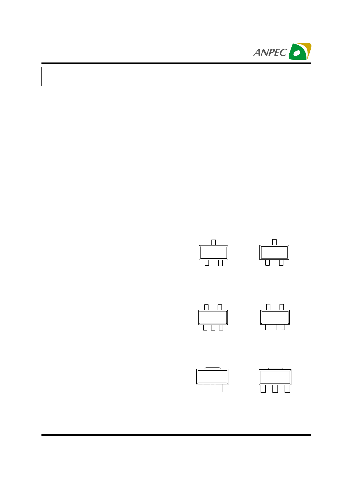
SOT-23 (T op V iew)
APL5309
GND
12
3
V
OUTVIN
APL5309
SOT-89 (T op View)
GND VINVOUT
123
TAB is GND
Features
The APL5308/9 series are micropower, low dropout
linear regulators, which operate from 2.7V to 6V input voltage and deliver up to 300mA. Typical dropout
voltage is only 400mV at 300mA loading. Designed
for use in battery-powered system, the low 60µA quiescent current makes it an ideal choice. Design with
an internal P-channel MOSFET pass transistor, the
APL5308/9 maintain a low supply current, independent of the load current and dropout voltage. Other
features include thermal-shutdown protection current
limit protection to ensure specified output current and
controlled short-circuit current. The APL5308/9 regu-
lators come in a miniature SOT-23, SOT-23-5 and
SOT-89 packages.
Applications
• 5V to 3.3~4.5V Linear Regulators
• 3.3V to 1.5~2.5V Linear Regulators
• CD-ROM, CD-R/W and DVD Player
• Networking System, LAN Card, ADSL/Cable
Modem, Cable Set-Top Box
• PC Peripherals
••
••
• Low Quiescent Current : 60µA (No load)
••
••
• Low Dropout Voltage : 400mV (@300mA)
••
••
• Fixed Output Voltage : 1.5V ~ 4.5V
by step 0.1V increment
••
••
• Stable with 1uF Output Capacitor
••
••
• Stable with Aluminum, Tantalum or Ceramic
Capacitors .
••
••
• No Protection Diodes Needed
••
••
• Built in Thermal Protection
••
••
• Built in Current Limit Protection
••
••
• Controlled Short Circuit Current : 50mA
••
••
• Fast Transient Response
••
••
• Short Setting Time
••
••
• SOT-23 ,SOT-23-5 and SOT-89 Packages
Pin Configuration
SOT-23 (T op V iew)
GND
12
3
V
OUT
V
IN
APL5308
General Description
V
IN
GND
V
OUT
NC
NC
123
45
SOT-23-5 (T op V iew)
APL5309
APL5308
SOT-89 (T op View)
GND VIN VOUT
123
TAB is V
IN
V
IN
GND V
OUT
NCNC
123
45
SOT-23-5 (T op V iew)
APL5308

Copyright ANPEC Electronics Corp.
Rev. A.5 - Apr., 2003
APL5308/9
www.anpec.com.tw2
Package Code
A : S O T -23 B : S O T -23 -5 D : SOT -89
Temp . Range
C : 0 to 7 0 C
Handling Code
TR : Tape & Reel
Voltage Code :
15 : 1.5V ~ 45 : 4.5V
APL5308/9 -
Handling Code
Temp . Range
Package Code
Voltage Code
APL5308/9
XXXXX 15
XXX XX - Date Code ; 15 - 1.5VAPL5308/9 -15 D :
Ordering and Marking Information
°
Product Name Marking Product Name Marking
APL5308-15A/B 389X APL5309-15A/B 399X
APL5308-16A/B 38AX APL5309-16A/B 39AX
APL5308-17A/B 38BX APL5309-17A/B 39BX
APL5308-18A/B 38CX APL5309-18A/B 39CX
APL5308-19A/B 38DX APL5309-19A/B 39DX
APL5308-20A/B 38EX APL5309-20A/B 39EX
APL5308-21A/B 38FX APL5309-21A/B 39FX
APL5308-22A/B 38GX APL5309-22A/B 39GX
APL5308-23A/B 38HX APL5309-23A/B 39HX
APL5308-24A/B 38IX APL5309-24A/B 39IX
APL5308-25A/B 38JX APL5309-25A/B 39JX
APL5308-26A/B 38KX APL5309-26A/B 39KX
APL5308-27A/B 38LX APL5309-27A/B 39LX
APL5308-28A/B 38MX APL5309-28A/B 39MX
APL5308-29A/B 38NX APL5309-29A/B 39NX
APL5308-30A/B 38OX APL5309-30A/B 39OX
APL5308-31A/B 38PX APL5309-31A/B 39PX
APL5308-32A/B 38QX APL5309-32A/B 39QX
APL5308-33A/B 38RX APL5309-33A/B 39RX
APL5308-34A/B 38SX APL5309-34A/B 39SX
APL5308-35A/B 38TX APL5309-35A/B 39TX
APL5308-43A/B 38UX APL5309-43A/B 39UX
APL5308-45A/B 38VX APL5309-45A/B 39VX
Marking Information
SOT-23 and SOT-23-5 packages
The last character “X” in the marking is for data code.
Copyright ANPEC Electronics Corp.
Rev. A.5 - Apr., 2003
APL5308/9
www.anpec.com.tw3
Pin Description
PIN
No. Name
I/O Description
1VINI Supply vol tage input.
2GND
Ground pins of the circuitry, and all ground pins must be soldered
To PCB with proper power dissipation.
3V
OUT
O Output pin of the regulator.
Symbol Parameter Rating Unit
VIN, V
OUT
Input Voltage or Out Voltage 6 V
SOT-23 357
SOT-23-5 357R
TH,JA
Thermal Resistance – Junction to Ambient
SOT-89 180
°C/W
P
D
Power Dissipation
Internally
W
T
J
Operating Junction Temperature °C
Control Section 0 to 125
Power Transistor 0 to 150
T
STG
Storage Temperature Range -65 to +150 °C
T
L
Lead Temperature (Soldering, 10 second) 260 °C
Absolute Maximum Ratings
Electrical Characteristics
Unless otherwise noted these specifications apply over full temperature, CIN=COUT=1µF, TJ=0 to 125°C.
Typical values refer to TJ=25°C.
APL5308/9
Symbol Parameter Test Conditions
Min. Typ. Max.
Unit
V
IN
Input Voltage 2.7 6 V
V
OUT
Output Voltage V
OUT
+1.0V< VCC<6.0V, 0mA< I
OUT
< I
MAX
V
OUT
-2
%
V
OUT
V
OUT
+2
%
V
I
LIMIT
Circuit Current Limit
V
IN=VOUT
+1V
650 mA
I
SHORT
Short Current V
OUT
=0V 50 mA
I
OUT
Load Current
V
IN=VOUT
+1V 300 mA
REG
LINE
Line Regulation V
OUT
+1V< VCC<6.0V, I
OUT
=1mA 1 10 mV
REG
LOAD
Load Regulation VIN =V
OUT
+1V, 0mA< I
OUT
< I
MAX
10
25
mV
Load Transient VIN= V
OUT
+1V , I
OUT
=1mA-300mA in 1µs150250mV
1.5V≤V
OUT
<2.0V 1 1.2
2.0V≤V
OUT
<2.5V 0.8 0.9
2.5V≤V
OUT
<3V 0.6 0.7
V
DROP
Dropout Voltage
(Note1)
I
OUT
=300mA
3V≤V
OUT
≤
3.5V 0.4 0.5
V
Copyright ANPEC Electronics Corp.
Rev. A.5 - Apr., 2003
APL5308/9
www.anpec.com.tw4
Electrical Characteristics (Cont.)
Unless otherwise noted these specifications apply over full temperature, CIN=COUT=1µF, TJ=0 to 125°C.
Typical values refer to T
J=25°C.
APL5308/9
Symbol Parameter Test Con ditions
Min. Typ. Max.
Unit
PSRR Ri pple Rejection
F≤1kHz, 1Vpp at V
IN
= V
OUT
+1.0V
45 55 dB
No load 60 100
I
Q
Quiescent Current
I
OUT
=300mA 450 500
µ
A
OTS
Over Temperature
150
°
C
Over Temperature
Hysteresis 30
°
C
TC
Output Voltage
Temperature
Coefficient
50 ppm/°C
C
OUT
Output Capaci tor 2.2
µ
F
ESR 0.01 0.1 1 Ohm
Note1 : Dropout voltage definition : VIN-VOUT when VOUT is 2% below the value of VOUT for VIN = VOUT+1V
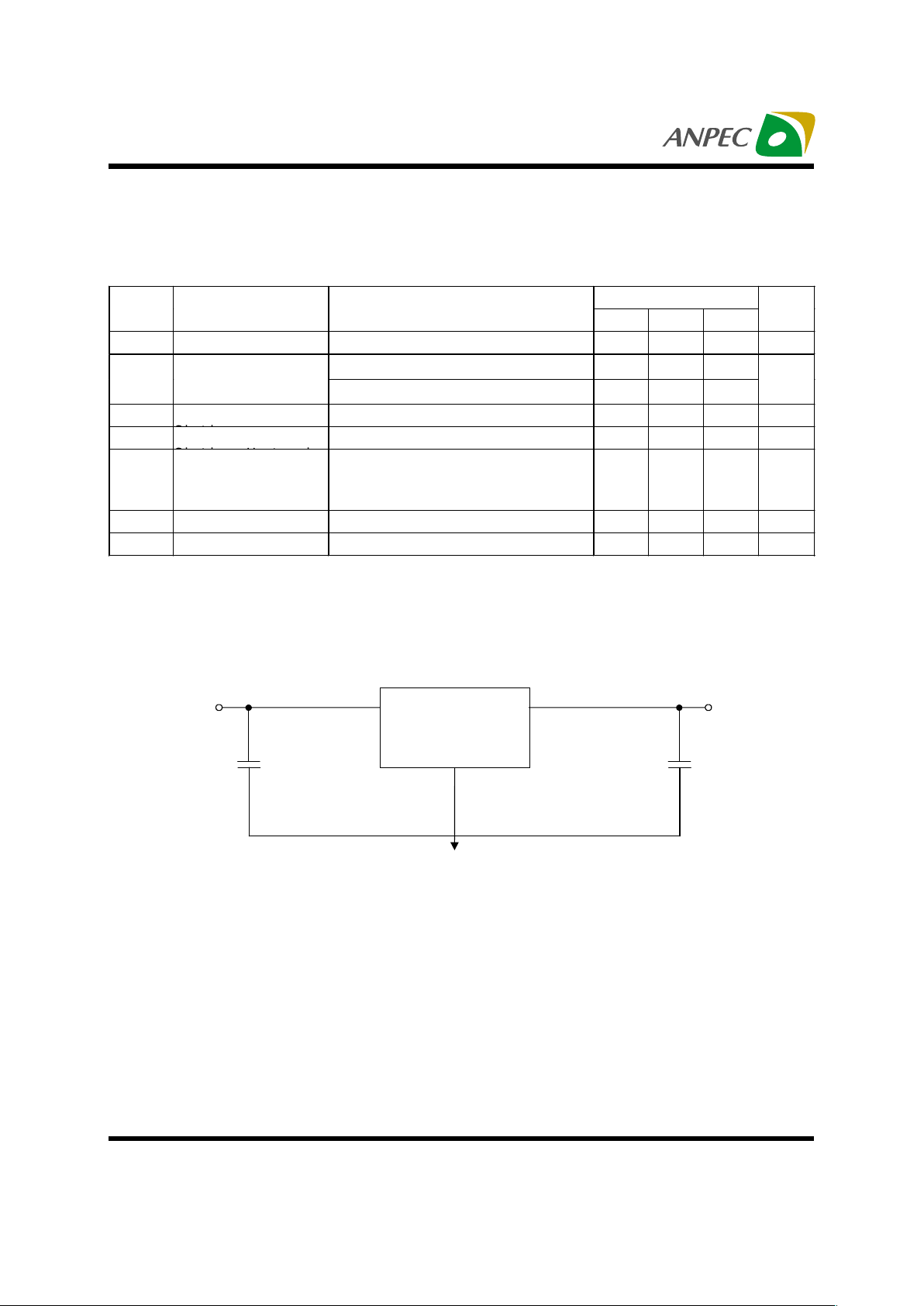
Application Circuit
V
OUT
V
IN
GND
VOUT
C
IN
1µF
APL5308/9
INP UT
2.7V to 6V
C
OUT
2.2µF
Copyright ANPEC Electronics Corp.
Rev. A.5 - Apr., 2003
APL5308/9
www.anpec.com.tw5
0
0.5
1
1.5
2
2.5
3
3.5
0123456
0
50
100
150
200
250
300
350
400
450
0 100 200 300 400 500
0
50
100
150
200
250
300
350
400
450
0123456
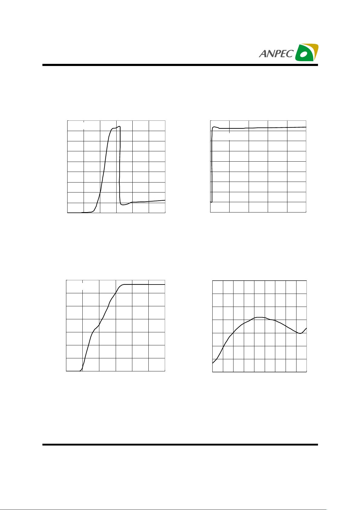
Typical Characteristics
Quiescent Current vs. Input Voltage
Input Voltage (V)
Quiescent Current (µA)
Quiescent Current vs. Output Current
Quiescent Current (µA)
Output Current (mA)
Output Voltage vs. Input V oltage
Input Voltage (V)
Output Voltage (V)
APL5308/9-33
VIN=5V
I
OUT
=0mA
APL5308/9-33
APL5308/9-33
I
OUT
=0mA
3.28
3.28
3.29
3.29
3.30
3.30
3.31
3.31
-40-200 20406080100120140
Output Voltage vs. Temperature
Temperature (°C )
Output Voltage (V)
APL5308/9-33

Copyright ANPEC Electronics Corp.
Rev. A.5 - Apr., 2003
APL5308/9
www.anpec.com.tw6
-8 0
+
0
-7 0
-6 0
-5 0
-4 0
-3 0
-2 0
-1 0
20 200
k
50 100 200500 1k 2k 5k10k20k50k100
k
0
100
200
300
400
500
600
700
800
0 100 200 300
Typical Characteristics
PSRR vs. Frequency
Frequency (H
Z)
PSRR (dB)
vIN =5V
IOUT =50mA
Output Current (mA)
Dropout Voltage (mV)
APL5308/9-33
Dropout Voltage vs. Output Current
Load-Transient Response
Output Voltage (100mV/div)
Time (100µs/div)
VOUT
Time (200µs/div)
Line-Transient Response
VIN=4.5V~5.5V
COUT=1µF
IOUT=10mA
Output Voltage (10mV/div)
APL5308/9-33
APL5308/9-33
VIN=5V
COUT=1µF
VOUT
IOUT=1mA~300mA
APL5308/9-33

Copyright ANPEC Electronics Corp.
Rev. A.5 - Apr., 2003
APL5308/9
www.anpec.com.tw7
SOT-23
Packaging Information
D
E H
S
e
A
A1
L
C
B
3
2
1
Millimeters Inches
Dim
Min. Max. Min. Max.
A 1.00 1.30 0.039 0.051
A1 0.00 0.10 0.000 0.004
B 0.35 0.51 0.014 0.020
C 0.10 0.25 0.004 0.010
D 2.70 3.10 0.106 0.122
E 1.40 1.80 0.055 0.071
e 1.90 BSC 0.075 BSC
H 2.40 3.00 0.094 0.118
L 0.37 0.0015

Copyright ANPEC Electronics Corp.
Rev. A.5 - Apr., 2003
APL5308/9
www.anpec.com.tw8
Packaging Information
SOT-23-5
e1
E1 E
b
12
3
45
e
D
A2
A
A1 L 2
L
L 1
a
Millimeters Inches
Dim
Min. Max. Min. Max.
A 0.95 1.45
0.037 0.057
A1 0.05 0.15
0.002 0.006
A2 0.90 1.30
0.035 0.051
D2.83.00
0.110 0.118
E2.63.00
0.102 0.118
E1 1.5 1.70
0.059 0.067
L 0.35 0.55
0.014 0.022
L1 0.20 BSC 0.008 BSC
L2 0.5 0.7
0.020 0.028
N5 5
α
0
°
10
°
0
°
10
°

Copyright ANPEC Electronics Corp.
Rev. A.5 - Apr., 2003
APL5308/9
www.anpec.com.tw9
SOT-89 (Reference EIAJ ED-7500A Reg stration SC-62)
Packaging Information
D
D1
e
B1
e1
B
123
L
H
E
C
a
a
A
Millimeters Inches
Dim
Min. Max. Min. Max.
A 1.40 1.60 0.055 0.063
B 0.40 0.56 0.016 0.022
B1 0.35 0.48 0.014 0.019
C 0.35 0.44 0.014 0.017
D 4.40 4.60 0.173 0.181
D1 1.35 1 .83 0 .053 0.072
e 1.50 BSC 0.059 BSC
e1 3.00 BSC 0.118 BSC
E 2.29 2.60 0.090 0.102
H 3.75 4.25 0.148 0.167
L 0.80 1.20 0.031 0.047
α
10
°
10
°
Copyright ANPEC Electronics Corp.
Rev. A.5 - Apr., 2003
APL5308/9
www.anpec.com.tw10
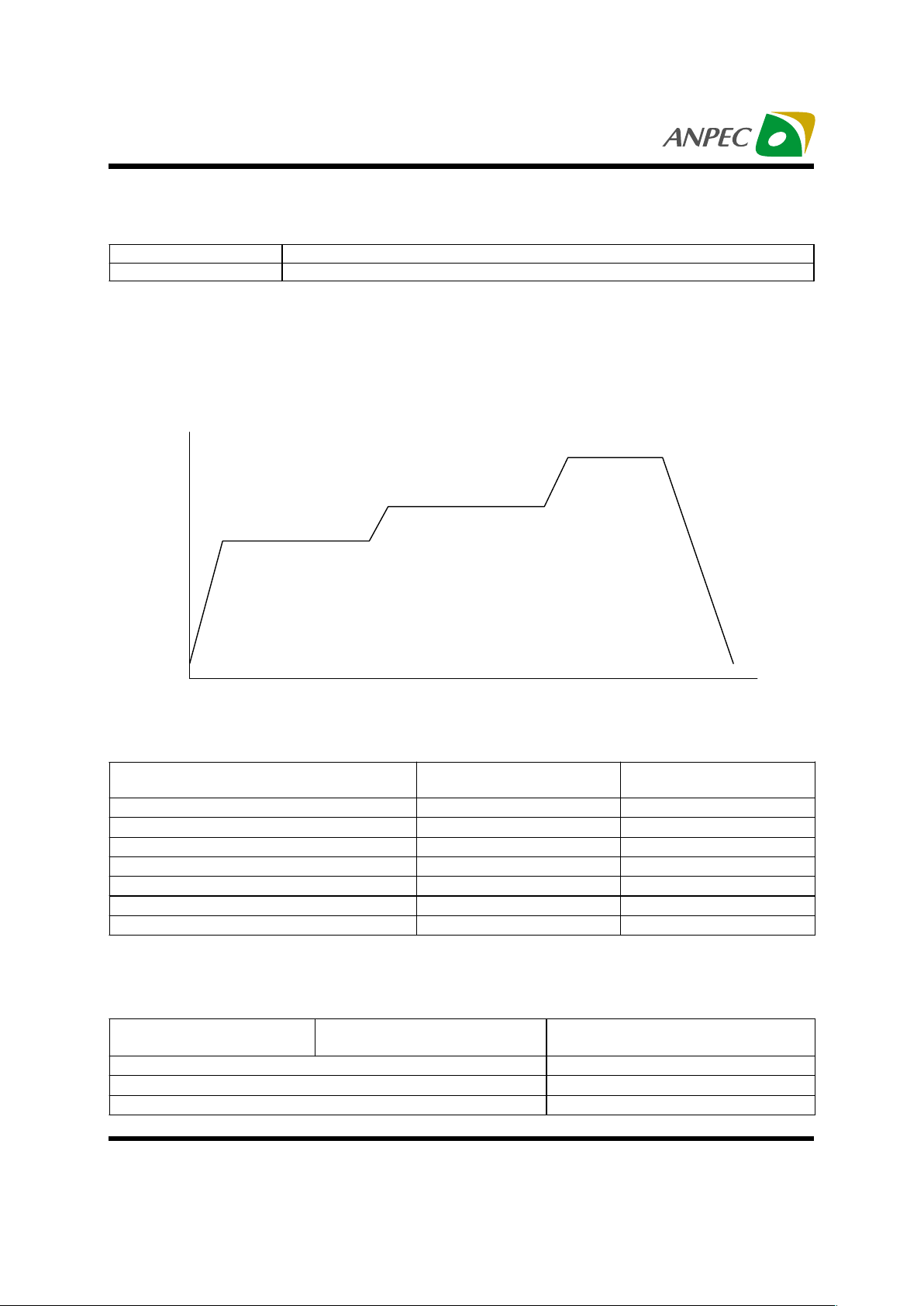
Physical Specifications
Pre-heat temperature
183 C
Peak temperature
Time
°
temperature
Classification Reflow Profiles
Convection or IR/
Convection
VPR
Average ramp-up rate(183°C to Peak) 3°C/second max. 10 °C /second max.
Preheat temperature 125 ± 25°C)
120 seconds max
Temperature maintained above 183°C
60 – 150 seconds
Time within 5°C of actual peak temperature
10 –20 seconds 60 seconds
Peak temperature range
220 +5/-0°C or 235 +5/-0°C 215-219°C or 235 +5/-0°C
Ramp-down rate
6 °C /second max. 10 °C /second max.
Time 25°C to peak temperature
6 minutes max.
Package Reflow Conditions
pkg. thickness
≥≥≥≥
2.5mm
and all bgas
pkg. thickness < 2.5mm and
pkg. volume
≥≥≥≥
350 mm³
pkg. thickness < 2.5mm and pkg.
volume < 350mm³
Convection 220 +5/-0 °C Convection 235 +5/- 0 °C
VPR 215-219 °C VPR 235 +5/-0 °C
IR/Convection 220 +5/-0 °C IR/Convection 235 +5/-0 °C
Terminal Material Solder-Plated Copper (Solder Material : 90/10 or 63/37 SnPb)
Lead Solderability Meets EIA Specification RSI86-91, AN SI/J-ST D -0 02 Category 3.
Reference JEDEC Standard J-STD-020A APRIL 1999
Reflow Condition (IR/Convection or VPR Reflow)

Copyright ANPEC Electronics Corp.
Rev. A.5 - Apr., 2003
APL5308/9
www.anpec.com.tw11
R e lia bility tes t p r o g ra m
Test item M ethod Description
SOLDERABILITY MIL-STD-883D-2003
245°C , 5 SEC
HO LT M IL-STD-883D-1005.7
1000 Hrs Bias @ 125 °C
PCT JESD-22-B, A102
168 Hrs, 100 % RH , 121°C
TST M IL-STD-883D-1011.9
-65°C ~ 150°C, 200 Cycles
ESD MIL-STD-883D-3015.7 VHBM > 2KV, VMM > 200V
La tc h -Up JE S D 78 10 ms , Itr > 100mA
Carrier Tape
A
J
B
T2
T1
C
t
Ao
E
W
Po
P
Ko
Bo
D1
D
F
P1
Application
A B C J T1 T2 W P E
178±160 ± 1.0 12 .0 2.5 ± 0.15 9.0 ± 0.5 1.4
8.0+ 0.3
- 0.3
4.0 1.75
F D D1 Po P1 Ao Bo Ko t
SOT-23
3.5 ± 0.05 1.5 +0.1
F
0.1MIN 4.0 2.0 ± 0.05 3.1 3.0 1.3 0.2±0.03
Application
A B C J T1 T2 W P E
178 ±172 ± 1.0 13.0 + 0.2 2.5 ± 0.15 8.4 ± 2 1 .5 ± 0.3 8 .0 ± 0.3 4 ± 0.1 1 .7 5± 0.1
F D D1 Po P1 Ao Bo Ko t
SOT-23-5
3.5 ± 0.05 1.5± 0.1 1.5± 0.1 4.0 ± 0.1 2 .0 ± 0.1 3.15 ± 0.1 3.2± 0.1 1.4± 0.1 0.2±0.033
Application
A B C J T1 T2 W P E
178 ±170 ± 213.5 ± 0.15 3 ± 0.15 14 ± 2 1.3 ± 0.3
12 + 0.3
12 - 0.1
8 ± 0.1 1 .7 5± 0.1
F D D1 Po P1 Ao Bo Ko t
SOT-89
5.5 ± 0.05 1.5± 0.1 1.5± 0.1 4.0 ± 0.1 2 .0 ± 0.1 4.8 ± 0.1 4.5± 0.1 1 .8 0± 0.1 0 .3±0.013

Copyright ANPEC Electronics Corp.
Rev. A.5 - Apr., 2003
APL5308/9
www.anpec.com.tw12
Application Carrier Width Cover Tape Width Devices Per Reel
SOT- 23
8 5.3 3000
SOT- 23-5
8 5.3 3000
SOT- 89
12 9.3 1000
Cover Tape Dimensions
Anpec Electronics Corp.
Head Office :
5F, No. 2 Li-Hsin Road, SBIP,
Hsin-Chu, T aiwan, R.O.C.
T el : 886-3-5642000
Fax : 886-3-5642050
Taipei Branch :
7F, No. 137, Lane 235, Pac Chiao Rd.,
Hsin Tien City, Taipei Hsien, Taiwan, R. O. C.
T el : 886-2-89191368
Fax : 886-2-89191369
Customer Service
 Loading...