


查询APA2069供应商
APA2120/2121
Stereo 2-W Audio Power Amplifier (with DC_Volume Control)
Features
• Low operating current with 14mA
• Improved depop circuitry to eliminate turn-on
and turn off transients in outputs
• High PSRR
• 32 steps volume adjustable by DC voltage w ith
hysteresis
• 2W pe r channel output power into 4Ω load at 5V,
BTL mode
• Two outpu t modes allowable with BTL and SE
modes selected by SE/BTL pin
• Low current consumption in shutdown mode
(50µA)
• Short C ircuit Protection
• Power off depop circuit integration
• TSSOP-24 with or without thermal pad package
General Description
APA2120/1 is a monolithic integrated circuit, which
provides precise DC volume control, and a stereo
bridged audio po wer amplifiers capable of producing
2. 7W(2.0W) into 3Ω with less than 10% (1.0%)
THD+N. The attenuator range of the volume control
in APA2120/1 is f rom 20dB (DC_Vol=0V) to -80dB
(DC_Vol=3.54V) wit h 32 steps. The advantage of
internal gain se tting can be less components and PCB
area. Both of the depop circuitry and the thermal
shut down protection circuitry are integrated in
APA2120/1, that reduce pops and clicks noise during power up or shutdown mode operation. It also
improves the power of f pop noise and protects the
chip from being destroyed by over temperature and
short current failure. To simplify the audio system
Applications
design, APA2120/1 combines a stereo bridge-tied
loads (BTL) mode for speaker drive and a stereo
• NoteBook PC
• LCD Monitor or TV
single-end (SE) mode for headphone drive into a
single chip, where both modes are easily switched
by the SE/BTL input control pin signal. Besides, the
multiple input selection is used for portable audio
system.
Ordering and Marking Information
APA2120/1
Lead Free Code
Handling Code
Temp. Range
Package Code
APA2120/1 R :
* TSSOP-P is a standard TSSOP package with a thermal pad exposure on the bottom of the package.
ANPEC reserves the right to make changes to improve reliability or manufacturability without notice, and advise
customers to obtain the latest version of relevant information to verify before placing orders.
Copyright ANPEC Electronics Corp.
Rev. A.1 - Mar., 2003
APA2120/1
XXXXX
Package Code
R : TSSOP-P *
Temp. Range
I : - 40 to 85 C
Handling Code
TU : Tube TR : Tape & Reel
TY : Tray
Lead Free Code
L : Lead Free Device Blank : Original Device
XXXXX - Date Code
°
www.anpec.com.tw1
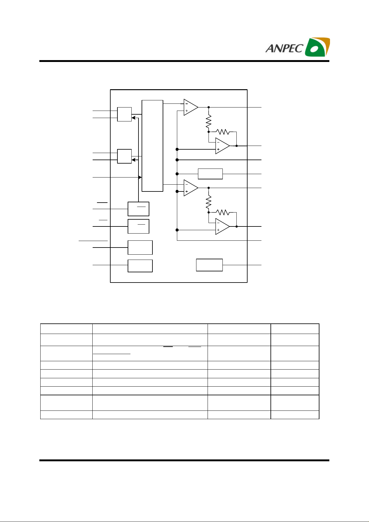
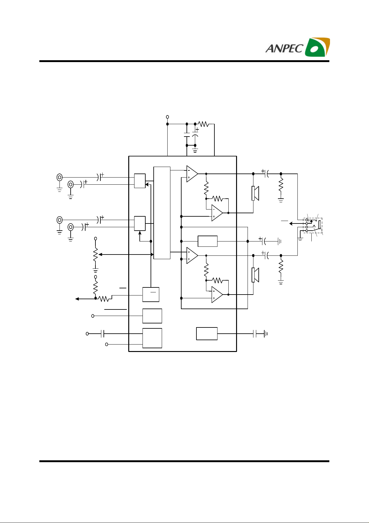
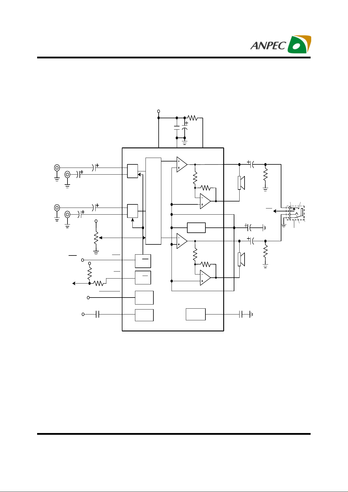
APA2120/2121
Block Diagram
LLINEIN
LHPIN
RLINEIN
RHPIN
VOLUME
HP/LINE
SE/BTL
SHUTDOWN
PCBEEP
MUX
MUX
HP/LINE
SE/BTL
Shutdown
ckt
PC-BEEP
ckt
Volume
Control
BYPASS
Clock Gen
LOUT+
LOUT-
LBYPASS
BYPASS
ROUT+
ROUT-
RBYPASS
CLK
For APA2121
Absolute Maximum Ratings
(Over operating free-air temperature range unless otherwise noted.)
Symbol Parameter Rating Unit
V
DD
V
IN
T
A
T
J
T
STG
T
S
V
ESD
P
D
Note:
1.APA2120/1 integrated internal thermal s hutdown protection when junction temperature ramp up to 150°C
2.Human body model: C=100pF, R=1500Ω, 3 positives pulse plus 3 negative pulses
3.Machine model: C=200pF, L=0.5µF, 3 positive pulses plus 3 negative pulses
Copyright ANPEC Electronics Corp.
Rev. A.1 - Mar., 2003
Supply Voltage Range -0.3 to 6 V
Input Voltage Range, SE/BTL, HP/LINE,
SHUTDOWN, PCBEN
-0.3 to VDD+0.3 V
Operating Ambient Temperature Range -40 to 85
Maximum Junction Temperature Intermal Limited*
1
Storage Temperature Range -65 to +150
Soldering Temperature,10 seconds 260
2
3
Electrostatic Discharge
-3000 to 3000*
-200 to 200*
Power Dissipation Intermal Limited
°
C
°
C
°
C
°
C
V
www.anpec.com.tw2
APA2120/2121
Typ.
Max.
Unit
Recommended Operating Conditions
Min. Max. Unit
Supply Voltage, V
DD
High level threshold voltage, V
Low level threshold voltage, V
Common mode input voltage, V
IH
SE/BTL , HP/LINE 4
SHUTDOWN, PCBEN 1.0
SHUTDOWN, PCBEN 2
IL
ICM
SE/BTL , HP/LINE 3
4.5 5.5 V
VDD-1.0 V
Thermal Characteristics
Symbol Parameter Value Unit
R
Thermal Resistance from Junction to Ambient in Free Air
THJA
TSSOP-P*
* 5 in2 printed circuit b oard with 2oz trace and copper pad through 9 25mil diameter vias.
45
The the rmal pad on the TSSOP_P package with solder on the printed circuit board.
Electrical Characteristics
VDD=5V, -20°C<TA<85 °C (unless otherwise noted)
°
C/W
V
V
Symbol Parameter Test Condition
VDD
Supply Voltage 4.5 5.5 V
SE/BTL=0V
IDD
ISD
IIH
IIL
V
OS
Copyright ANPEC Electronics Corp.
Rev. A.1 - Mar., 2003
Supply Current
Supply Current in Shutdown
Mode
SE/BTL=5V
SE/BTL=5V
SHUTDOWN=0V
High input Current 900 nA
Low Input Current 900 nA
Output Differential Voltage 5 mV
APA2120/1
Min.
14 25
8.0 15
50
www.anpec.com.tw3
mA
µ
A
APA2120/2121
Electrical Cha racteristics (Cont.)
Operating Chara cteristics, BTL mode
VDD=5V,TA=25°C,RL=4Ω, Gain=2V/V (unless otherwise noted)
Symbol Parameter Test Condition
THD=10%, RL=3Ω, Fin=1kHz
THD=10%, RL=4Ω, Fin=1kHz
PO
THD+N
PSRR
Maximum Output Power
Total Harmonic Distortion Plus
Noise
Power Ripple Rejection Ratio
THD=10%, RL=8Ω, Fin=1kHz
THD=1%, RL=3Ω, Fin=1kHz
THD=1%, RL=4Ω, Fin=1kHz
THD=0.5%, RL=8Ω, Fin=1kHz
PO=1.5W, RL=4Ω, Fin=1kHz
PO=1W, RL=8Ω, Fin=1kHz
VIN=0.1Vrms, RL=8Ω, CB=1µF,
Fin=120Hz
APA2120/1
Min. Typ. Max.
2.7
2.3
1.5
2.0
1.9
1 1.1
0.05
0.07
60 dB
Unit
W
%
Xtalk
S/N
Channel Separation
Signal to Noise Ratio
CB=1µF, RL=8Ω, Fin=1kHz
PO=1.1W, RL=8Ω, A_wieght
Operating Characteristics, SE mode
VDD=5V,TA=25°C,RL=4Ω, Gain=1V/V (unless otherwise noted)
Symbol Parameter Test Condition
THD=10%, RL=8Ω, Fin=1kHz
THD=10%, RL=32Ω, Fin=1kHz
P
O
Maximum Output Power
THD=1%, RL=8Ω, Fin=1kHz
THD=1%, RL=32Ω, Fin=1kHz
THD+N
PSRR
Xtalk
S/N
Total Harmonic Distortion Plus
Noise
Power Ripple Rejection Ratio
Channel Separation
Signal to Noise Ratio
PO=250mW, RL=8Ω, Fin=1kHz
PO=75mW, RL=32Ω, Fin=1kHz
VIN=0.1Vrms, RL=8Ω, CB=1µF,
Fin=120Hz
CB=1µF, RL=32Ω, Fin=1kHz
PO=75mW, SE, RL=32Ω, A_wieght
90 dB
95 dB
APA2120/1
Min. Typ. Max.
400
110
320
90
0.08
0.08
48 dB
100
100 dB
Unit
mW
%
dB
Copyright ANPEC Electronics Corp.
Rev. A.1 - Mar., 2003
www.anpec.com.tw4
APA2120/2121
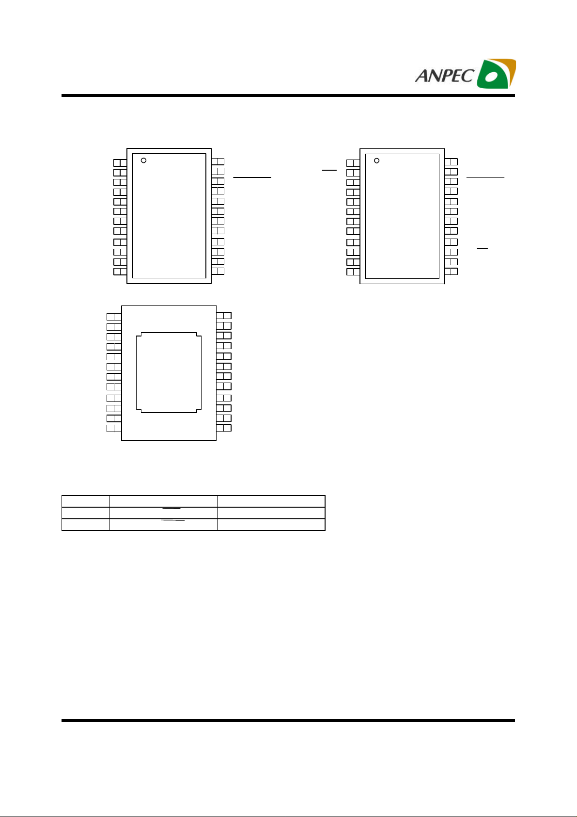
Pin Description
GND
PCBEN
VOLUME
LOUT+
LLINEIN
LHPIN
PVDD
RBYPASS
LOUT-
LBYPASS
BYPASS
GND
1
2
3
4
5
6
7
8
9
10
11
12
APA2120
TOP View
Thermal
Pad
24
23
22
21
20
19
18
17
16
15
14
13
GND
RLINEIN
SHUTDOWN
ROUT+
RHPIN
VDD
PVDD
CLK
ROUTSE/BTL
PC-BEEP
GND
GND
HP/LINE
VOLUME
LOUT+
LLINEIN
LHPIN
PVDD
RBYPASS
LOUT-
LBYPASS
BYPASS
GND
1
2
3
4
5
6
7
8
9
10
11
12
APA2121
TOP View
24
23
22
21
20
19
18
17
16
15
14
13
GND
RLINEIN
SHUTDOWN
ROUT+
RHPIN
VDD
PVDD
CLK
ROUTSE/BTL
PC-BEEP
GND
APA2120/1
Bottom View
Multiple Input Selection PCBEEP Control Input
APA2120 SE/BTL PCBEN
APA2121 HP/LINE -
Copyright ANPEC Electronics Corp.
Rev. A.1 - Mar., 2003
www.anpec.com.tw5
APA2120/2121
Pin Function Description
Pin
Name No
GND
PCBEN 2 I/P BEEP mode control input, active H, for APA2120 only
HP/LINE 2 I/P
VOLUME 3 Input signal for internal volume gain setting.
LOUT+ 4 O/P
LLINEIN 5 I/P
LHPIN 6 O/P
PVDD 7,18 Supply voltage only for power amplifier.
RBYPASS 8 I/P Right channel bypass voltage.
LOUT- 9 O/P
LBYPASS 10 I/P
BYPASS 11 Bias voltage generator
PC_BEEP
SE/BTL 15 I/P
ROUT- 16 O/P
CLK 17 Clock signal generator
VDD 19
RHPIN 20 I/P
ROUT+ 21 O/P
SHUTDOWN 22 I/P
RLINEIN 23 I/P
1,12,
13,24
Config.
14 I/P
Description
Ground connection, Connected to thermal pad.
Multi-input selection input, headphone mode when held high, line-in
mode when held low for APA2121 only.
Left channel positive output in BTL mode and SE mode.
Left channel line input terminal, selected when HP/LINE is held low.
Left channel headphone input terminal, selected when HP/LINE is
held high.
Left channel negative output in BTL mode and high impedance in
SE mode.
Left channel bias voltage generator.
PCBEP signal input
Output mode control input, high for SE output mode and low for
BTL mode.
Right channel negative output in BTL mode and high impedance in
SE mode.
Supply voltage for internal circuit excepting power amplifier.
Right channel headphone input terminal, selected when HP/LINE is
held high.
Right channel positive output in BTL mode and SE mode.
It will be into shutdown mode when pull low.
Right channel line input terminal, selected when HP/LINE is held
low.
Copyright ANPEC Electronics Corp.
Rev. A.1 - Mar., 2003
www.anpec.com.tw6
APA2120/2121
Control Input Ta ble
For APA2120
SE/BTL SHUTDOWN PC-BEEP Operating mode
X L Disable Shutdown mode
L H Disable Line input, BTL out
H H Disable HP input, SE out
X X Enable PCBEEP input, BTL out
For APA2121
SE/BTL HP/LINE SHUTDOWN PC-BEEP Operating mode
X X L Disable Shutdown mode
L L H Disable Line input, BTL out
L H H Disable HP input, BTL out
H L H Disable Line input, SE out
H H H Disable HP input, BTL out
X X X Enable PCBEEP input, BTL out
Copyright ANPEC Electronics Corp.
Rev. A.1 - Mar., 2003
www.anpec.com.tw7
APA2120/2121
Typical Application Circuit
APA2120
L-LINE
R-LINE
L-HP
R-HP
1µF
1µF
50kΩ
100kΩ
1µF
1µF
VDD
VDD
100kΩ
LLINEIN
LHPIN
RLINEIN
RHPIN
VOLUME
SE/BTL
MUX
MUX
SE/BTL
VDD
0.1µF
VDD PVDDGND
Volume
Control
0Ω
100µF
BYPASS
LOUT+
LOUT-
LBYPASS
BYPASS
ROUT+
ROUT-
4Ω
2.2µF
4Ω
220µF
220µF
SE/BTL
1kΩ
1kΩ
Control
Pin
Headphone Jack
Tip
Ring
Sleeve
Shutdown
SHUTDOWN
Signal
0.47µF
BEEP
Signal
PCBEN
PCBEEP
PCBEN
Signal
Copyright ANPEC Electronics Corp.
Rev. A.1 - Mar., 2003
Shutdown
ckt
PC-BEEP
ckt
Clock Gen
RBYPASS
CLK
47nF
www.anpec.com.tw8
APA2120/2121
Typical Application Circuit
APA2121
L-LINE
R-LINE
L-HP
R-HP
HP/LINE
Signal
1µF
1µF
100kΩ
1µF
1µF
50kΩ
VDD
100kΩ
LLINEIN
RLINEIN
VOLUME
HP/LINE
VDD
SE/BTL
LHPIN
RHPIN
MUX
MUX
HP/LINE
SE/BTL
VDD
VDD PVDDGND
Volume
Control
0Ω
100µF0.1µF
BYPASS
LOUT+
LOUT-
LBYPASS
BYPASS
ROUT+
ROUT-
4Ω
2.2µF
4Ω
220µF
220µF
SE/BTL
1kΩ
1kΩ
Control
Pin
Headphone Jack
Ring
Sleeve
Tip
Shutdown
SHUTDOWN
Signal
BEEP
Signal
PCBEEP
0.47µF
Copyright ANPEC Electronics Corp.
Rev. A.1 - Mar., 2003
Shutdown
ckt
PC-BEEP
ckt
Clock Gen
RBYPASS
CLK
47nF
www.anpec.com.tw9
APA2120/2121
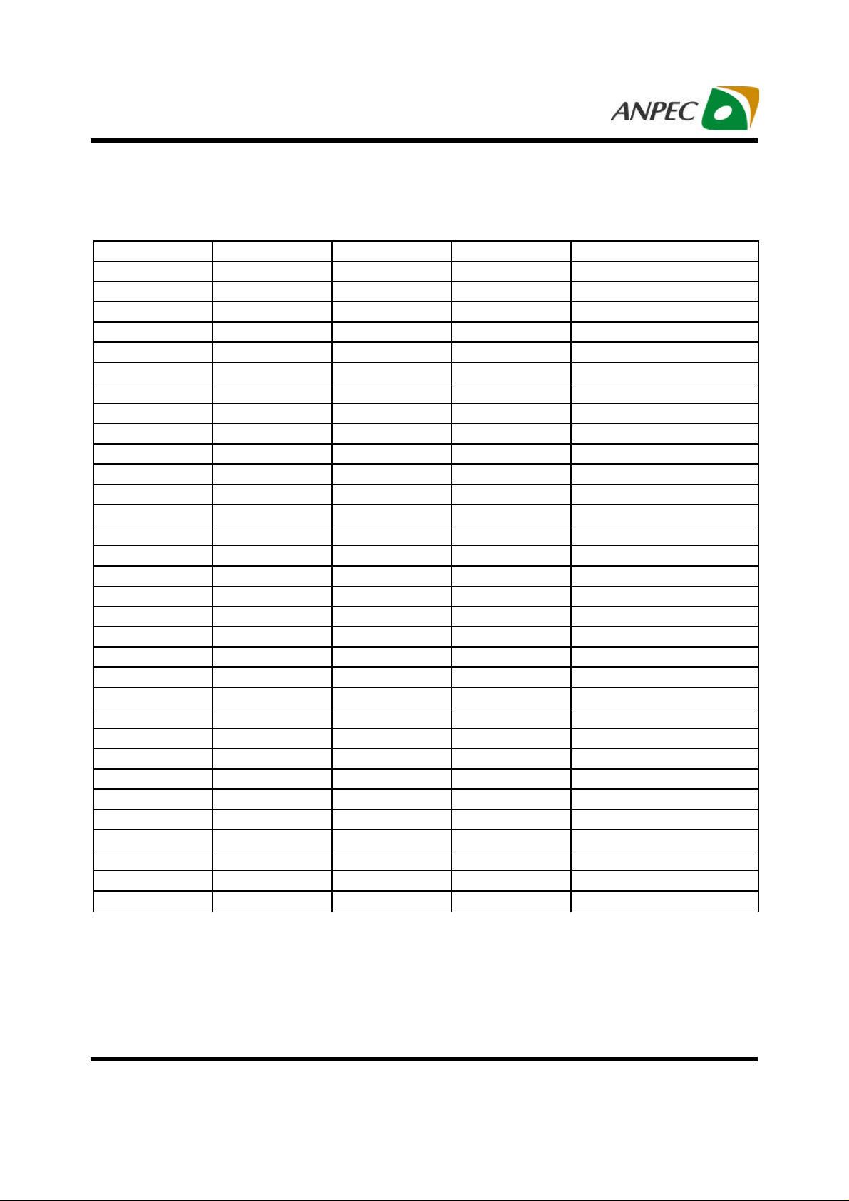
Volume Control Table_BTL Mode
Supply Voltage Vdd=5V
Gain(dB) High(V) Low(V) Hysteresis(mV) Recommended Voltage(V)
20 0.12 0.00 0
18 0.23 0.17 52 0.20
16 0.34 0.28 51 0.31
14 0.46 0.39 50 0.43
12 0.57 0.51 49 0.54
10 0.69 0.62 47 0.65
8 0.80 0.73 46 0.77
6 0.91 0.84 45 0.88
4 1.03 0.96 44 0.99
2 1.14 1.07 43 1.10
0 1.25 1.18 41 1.22
-2 1.37 1.29 40 1.33
-4 1.48 1.41 39 1.44
-6 1.59 1.52 38 1.56
-8 1.71 1.63 37 1.67
-10 1.82 1.74 35 1.78
-12 1.93 1.85 34 1.89
-14 2.05 1.97 33 2.01
-16 2.16 2.08 32 2.12
-18 2.28 2.19 30 2.23
-20 2.39 2.30 29 2.35
-22 2.50 2.42 28 2.46
-24 2.62 2.53 27 2.57
-26 2.73 2.64 26 2.69
-28 2.84 2.75 24 2.80
-30 2.96 2.87 23 2.91
-32 3.07 2.98 22 3.02
-34 3.18 3.09 21 3.14
-36 3.30 3.20 20 3.25
-38 3.41 3.32 18 3.36
-40 3.52 3.43 17 3.48
-80 5.00 3.54 16 5
Copyright ANPEC Electronics Corp.
Rev. A.1 - Mar., 2003
www.anpec.com.tw10

APA2120/2121
Typical Characteristics
THD+N vs. Frequency
10
VDD=5V
RL=3Ω
Po=1.75W
BTL
1
THD+N (%)
0.1
0.01
20 20k100 1k
AV=10
Frequency (Hz)
THD+N vs. Frequency
10
VDD=5V
RL=4Ω
Po=1.5W
BTL
AV=2
AV=5
THD+N vs. Output Power
10
VDD=5V
RL=3Ω
AV=2
BTL
1
THD+N (%)
0.1
0.01
10m 3100m 1 2
f=20kHz
f=1kHz
f=20Hz
Output Power (W )
THD+N vs. Output Power
10
VDD=5V
RL=4Ω
AV=2
BTL
1
0.1
THD+N (%)
0.01
20 20k50 100 200 500 1k 2k 5k
AV=2
AV=5
AV=10
Frequency (W)
Copyright ANPEC Electronics Corp.
Rev. A.1 - Mar., 2003
1
f=20kHz
THD+N (%)
0.1
0.01
100m 3200m 500m 800m 2
f=1kHz
f=20Hz
Output Power (W )
www.anpec.com.tw11

APA2120/2121
Typical Characte ristics (Cont.)
THD+N vs. Frequency
10
VDD=5V
RL=8Ω
Po=1.0W
BTL
1
THD+N (%)
0.1
0.01
20 20k100 1k
AV=2
AV=5
AV=10
Frequency (Hz)
THD+N vs. Frequency
10
VDD=5V
RL=8Ω
Po=250mW
SE
THD+N vs. Output Power
10
VDD=5V
RL=8Ω
AV=2
BTL
1
f=20kHz
0.1
THD+N (%)
f=1kHz
f=20Hz
0.01
10m 2100m 1
Output Power (W )
THD+N vs. Output Power
10
VDD=5V
RL=8Ω
AV=2
BTL
1
AV=5
THD+N (%)
0.1
0.01
20 20k100 1k
AV=1
AV=2.5
Frequency (Hz)
Copyright ANPEC Electronics Corp.
Rev. A.1 - Mar., 2003
1
f=20kHz
0.1
THD+N (%)
f=20Hz
f=1kHz
0.01
10m 500m
100m
Output Power (W )
www.anpec.com.tw12

APA2120/2121
Typical Characte ristics (Cont.)
THD+N vs. Frequency
10
VDD=5V
RL=16Ω
Po=100mW
SE
1
THD+N (%)
AV=2
0.1
0.01
20 20k50 100 200 500 1k 2k 5k
AV=1
AV=2.5
Frequency (Hz)
THD+N vs. Frequency
10
VDD=5V
RL=32Ω
Po=75mW
SE
1
THD+N vs. Output Power
10
VDD=5V
RL=16Ω
AV=1
BTL
1
f=20Hz
THD+N (%)
0.1
0.01
10m 300m
f=20kHz
f=1kHz
100m
Output Power (W )
THD+N vs. Output Power
10
VDD=5V
5
RL=32Ω
AV=1
BTL
1
f=20kHz
THD+N (%)
0.1
0.01
20 20k100 1k
AV=2.5
AV=1
AV=5
Frequency (Hz)
Copyright ANPEC Electronics Corp.
Rev. A.1 - Mar., 2003
THD+N (%)
0.01
f=20Hz
0.1
f=1kHz
10m 200m50m 100m
Output Power (W )
www.anpec.com.tw13

APA2120/2121
Typical Characte ristics (Cont.)
THD+N vs. Frequency
10
VDD=5V
RL=10Ω
Vo=1VRMS
SE
1
THD+N (%)
0.1
0.01
20 20k100 1k
AV=2.5
AV=1
AV=5
Frequency (Hz)
Crosstalk vs. Frequency
+0
VDD=5V
RL=8Ω
Po=1.0W
-20
AV=2
BTL
-40
THD+N vs. Output Sw ing
10
VDD=5V
RL=10Ω
AV=1
SE
1
THD+N (%)
0.1
0.01
100m 3500m
Output Sw ing (VRMS)
Crosstalk vs. Frequency
+0
VDD=5V
RL=32Ω
Po=75mW
-20
AV=1
SE
-40
f=1kHz
f=20kHz
f=20Hz
1
2
-60
-80
Crosstalk (dB)
-100
-120
20 20k100 1k
R-ch to L-ch
Frequency (Hz)
Copyright ANPEC Electronics Corp.
Rev. A.1 - Mar., 2003
L-ch to R-ch
-60
-80
Crosstalk (dB)
-100
-120
R-ch to L-ch
20 20k100 1k
Frequency (Hz)
L-ch to R-ch
www.anpec.com.tw14

APA2120/2121
Typical Characte ristics (Cont.)
Noise Floor vs. Freq uency
100u
50u
20u
10u
5u
Noise Floor (µVRMS)
2u
1u
20 20k100 1k
Frequency (Hz)
Noise Floor vs. Freq uency
100u
VDD=5V
RL=10KΩ
50u
AV=1
SE
20u
10u
5u
Noise Floor (µVRMS)
2u
1u
20 20k100 1k
No Filter
A-Weight
No Filter
A-Weight
VDD=5V
RL=8Ω
AV=2
BTL
Noise Floor vs. Freq uency
100u
VDD=5V
RL=32Ω
50u
AV=1
SE
20u
No Filter
10u
5u
A-Weight
Noise Floor (µVRMS)
2u
1u
20 20k100 1k
Frequency (Hz)
Power Dissipation vs. Output Pow er
0.2
0.18
0.16
0.14
0.12
0.1
0.08
0.06
Power Dissipation (W)
RL=32Ω
0.04
0.02
0
0 0.05 0.1 0.15 0.2 0.25 0.3 0.35 0.4
RL=16Ω
RL=8Ω
VDD=5V
AV=1
SE
Frequency (Hz)
Copyright ANPEC Electronics Corp.
Rev. A.1 - Mar., 2003
Output Power (W )
www.anpec.com.tw15

APA2120/2121
Typical Characte ristics (Cont.)
Power Dissipation vs. Output Pow er
1.8
1.6
1.4
1.2
1
0.8
0.6
0.4
Power Dissipation (W)
0.2
0
0 0.5 1 1.5 2 2.5
RL=8Ω
RL=3Ω
RL=4Ω
Output Power (W )
Output Po wer vs. Supply Voltage
VDD=5V
AV=2
BTL
Supply Current vs. Supply Voltage
20
17.5
15
12.5
10
7.5
5
Suuply Current (mA)
2.5
1 1.5 2 2.5 3 3.5 4 4.5 5 5.5
BTL
SE
Supply Vo ltage (V)
Output Po wer vs. Supply Voltage
No Load
2.0
RL=8Ω
1.8
AV=2
BTL
1.6
1.4
1.2
1.0
0.8
0.6
Output Power (W)
0.4
0.2
0
2.5 3 3.5 4 4.5 5 5.5
THD+N=10%
THD+N=1%
Supply Vo ltage (V)
Copyright ANPEC Electronics Corp.
Rev. A.1 - Mar., 2003
160
RL=32Ω
AV=1
140
SE
120
100
80
60
40
Output Power (mW)
20
0
2.5 3 3.5 4 4.5 5 5.5
THD+N=10%
THD+N=1%
Supply Vo ltage (V)
www.anpec.com.tw16

APA2120/2121
Typical Characte ristics (Cont.)
Output Pow er vs. Load Resistance
3
VDD=5V
AV=2
BTL
2.5
2
1.5
1
Output Power (W)
0.5
THD+N=1%
0
4 8 121620242832 36404448525660 64
THD+N=10%
Load Resistance (Ω)
Close Loop Response
+12
VDD=5V
RL=8Ω
AV=2
+10
BTL
CO=330µF
+8
Output Pow er vs. Load Resistance
0.7
VDD=5V
AV=1
0.6
SE
0.5
0.4
0.3
0.2
Output Power (W)
0.1
THD+N=1%
0
4 8 12 16 20 24 28323640 44485256 6064
THD+N=10%
Load Resistance (Ω)
Close Loop Response
+6
VDD=5V
RL=32Ω
AV=1
+4
SE
CO=330µF
+2
+6
AV=2
+4
Loop Gain (dB)
+2
-0
20 20k100 1k
AV=5
AV=10
Frequency (Hz)
Copyright ANPEC Electronics Corp.
Rev. A.1 - Mar., 2003
+0
AV=1
-2
Loop Gain (dB)
-4
-6
20 20k100 1k
AV=2.5
AV=5
Frequency (Hz)
www.anpec.com.tw17

APA2120/2121
Typical Characte ristics (Cont.)
PSRR vs. Freq uency
+0
-20
-40
-60
-80
TT
VDD=5V
Vin=100mVRMS
RL=8Ω
Cbypass=2.2µF
BTL
SE
Ripple Rejection Ratio (dB)
20 20k100 1k
Frequency (Hz)
Copyright ANPEC Electronics Corp.
Rev. A.1 - Mar., 2003
www.anpec.com.tw18

APA2120/2121
Application Descriptions
BTL Operation
The APA2120/1 output stage (power amplif ier) has
two pairs of ope rational amplifiers internally, allowed
for d ifferent amplifier configurations.
OUT+
Volume Control
amplifier output
signal
Circuit
Vbias
OP1
RL
OUT-
OP2
Figure 1: APA2120/1 internal configuration
(each channel)
The po wer amplifier’s OP1 gain is setting by intern al
unity-gain and input audio signal is come from internal volume co ntrol amplifier, while the second amplifier OP2 is internally fixed in a unity-gain, inverting
configuration. Figure 1 shows that the output of OP1
is co nnected to the input to OP2, which results in the
output signals of w ith both amplifiers with identical in
magnitude, but out of phase 180°. Consequently,
the differential gain for each channel is 2 x (Gain of
SE mode).
By d riving the load differentially through outputs OUT+
and OUT-, an amplifier configuration commonly re-
BTL Operation (Cont.)
Four times the output power sa me conditions. A BTL
configuration, such as the one used in APA2120/1,
also creates a second advantage over SE amplifiers.
Since the differential outputs, ROUT+, RO UT-,
LOUT+, and LOUT-, are biased at half-supply, no
need DC voltage exists across the load. This eliminates the need for an output coup ling capacitor which
is required in a single supply, SE configuration.
Single-Ended Operation
Consider the single-supply SE configuration shown
Application Circuit. A cou pling capacitor is required
to block the DC offse t voltage from reaching the load.
These cap acitors can be quite large (approximately
33µF to 1000µF) so they tend to be expensive, occupy valuable PCB area, and have the additional
drawback of limiting low-frequency perf ormance of
the system (refer to the Output Coupling Capacitor).
The rules described still hold with the addition of the
following relationship:
1
Cbypass x 125kΩ
1
≤
RiCi
<<
1
R LCC
(1)
Output SE/BTL Operation
ferred to as bridged mode is established. BTL mode
operation is different from the classical single-ended
SE amplifier configuration where one side of its load
is connected to ground.
A BTL amplifier design h as a few distinct advantages
over the SE configuration, as it provides differential
drive to the load, thus doubling the output swing for a
specified supply voltage.
Copyright ANPEC Electronics Corp.
Rev. A.1 - Mar., 2003
The ability of the APA2120/1 to easily switch between
BTL and SE modes is o ne of its most important costs
saving features. This feature eliminates the requirement for an add itional headphone amplifier in applications w here internal stereo speakers are driven in
BTL mode bu t external headphone or speakers must
be accommodated.
www.anpec.com.tw19

APA2120/2121
Application Descriptions (Cont.)
Output SE/BTL Ope ration (Cont.) Output SE/BTL Operation (Cont.)
Internal t o the APA2120/1, two separate amplifiers
drive OUT+ and OUT- (see Figure 1). The SE/BTL
input controls the operation of the follower amplifier
that drives LOUT- and ROU T-.
• When SE/BTL is held low, the OP2 is turn on and
the APA2120/1 is in the BTL mode.
• When SE/ BTL is held high, the OP2 is in a high
out put impedance state, which configures the
APA2120/1 as SE driver from OUT+. IDD is reduced
by app roximately one-half in SE mode.
Control of the SE/BTL input can be a logic-level TTL
source or a resistor divider network or the stereo
headphone jack with switch pin as shown in Application Circuit.
1kΩ
VDD
100kΩ
Control
Pin
Ring
Resistor 1 kΩ then pulls low the SE/BTL pin, enabling
the BTL function.
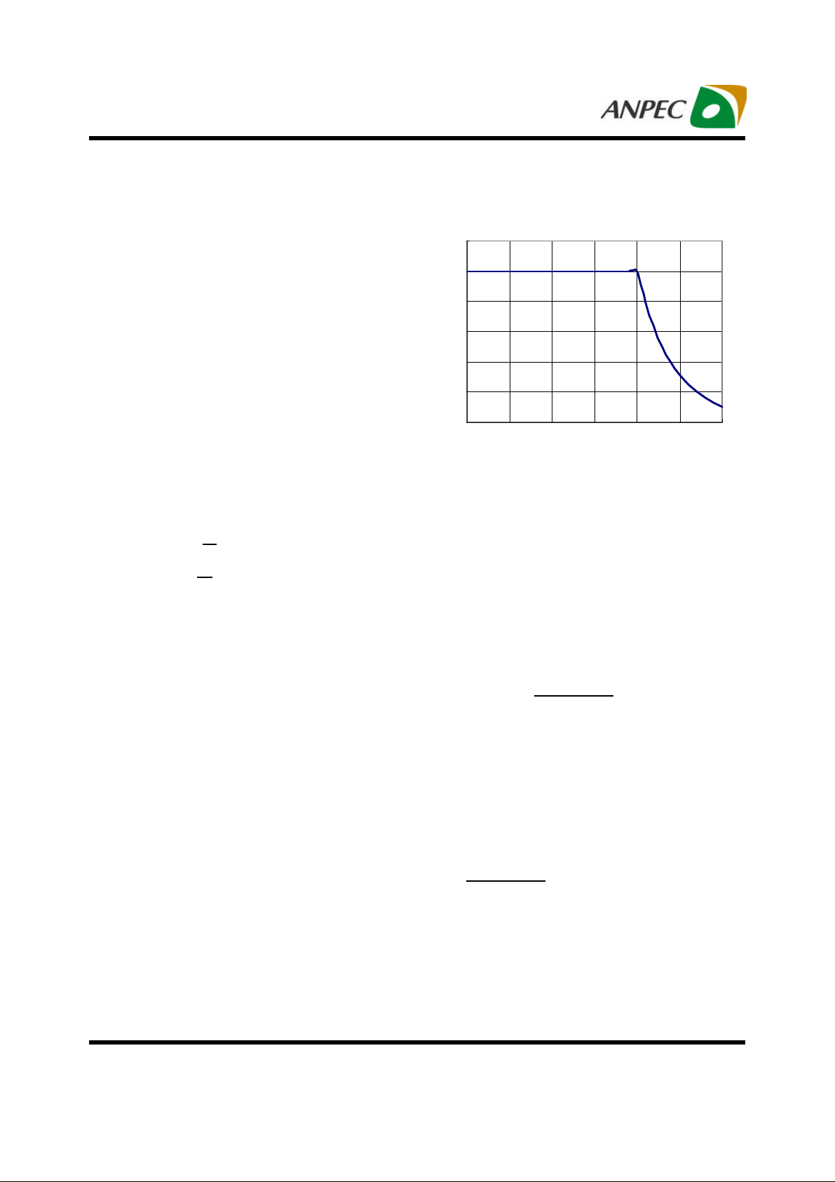
Volume Control Function
APA2120/1 has an internal stereo volume control
whose setting is a function of th e DC voltage applied
to the VOLUME input pin. The APA2120/1 volume
control consists of 32 steps that are individually selected by a variable DC voltage level on the VOLUME control pin. The range of the steps, controlled
by the DC voltage, are from 20dB to -80dB. Each
gain step corresponds to a specific input voltage
range, as shown in table. To minimize the effect of
noise on the volume con trol pin, which can affect the
selected gain level, hysteresis and clock delay are
implemented. The amount of hysteresis co rresponds
to half of the step w idth, as shown in volume control
SE/BTL
Sleeve
Tip
Headphone Jack
Figure 2: SE/BTL input selection by phonejack plug
In Figure 2, input SE/BTL operates as follows :
When the phonejack plug is inserted, the 1kΩ resistor is disconnected and the SE/BTL input is pulled
high and e nables the SE mode. When the input goes
high, the OUT- amplifier is shutdown causing the
speaker to mute. The OUT+ amplifier then drives
through the output capacitor (CC) into the headp hone
jack. When there is no headphone plugged into the
system, the contact pin of the h eadphone jack is connecte d from the signal pin, the voltage divider set up
by resistors 100kΩ and 1kΩ.
Copyright ANPEC Electronics Corp.
Rev. A.1 - Mar., 2003
graph.
Gain_BTL mode
20
16
12
8
4
0
-4
-8
-12
-16
-20
-24
-28
-32
-36
-40
-44
0 0.2 0.4 0.6 0.8 1 1.2 1.4 1.6 1.8 2 2.2 2.4 2.6 2.8 3 3.2 3.4 3.6 3.8
APA2021 volume control curve
Figure 3: Gain setting vs VOLUME pin voltage
www.anpec.com.tw20
Forward
Backward
(V)
APA2120/2121
Application Descriptions (Cont.)
Volume Control Function (Cont.)
For highest accuracy, the voltage shown in the ‘recommended voltage’ column of the table is used to
select a desired gain. This recommended voltage is
exactly halfway between the tw o nearest transitions.
The gain levels are 2dB/step from 20dB to -40 dB in
BTL mode, and the last step at -80dB a s mute mode.
Input Resistance, Ri
The gain f or each audio input of the APA2120/1 is
set by the int ernal resistors (Ri and Rf) of volume
control amplifier in inverting configura tion.
SE Gain =
BTL Gain
RF
-
=
AV
Ri
RF
-2 x
=
Ri
(2)
(3)
BTL mode op eration brings the factor of 2 in the gain
equation due to the inverting amplifier mirroring the
voltage swing across the load. For the varying gain
setting, APA2120/1 gene rates each input resistance
on figure 4. The input resistance will affect the low
Ri(kΩ)
120
100
80
60
40
20
0
-40 -30 -20 -10 0 10 20
Ri vs Gain(BTL)
Gain(dB)
Figure 4: Input resistance vs Gain setting
Input Capacitor, Ci
In th e typical application an input capacitor, Ci, is required to allow the a mplifier to bias the input signal to
the proper DC level for optimum operation. In this
case, Ci and the minimum input impedance Ri (10kΩ)
form a high-pass filter w ith the corner frequency determined in th e follow equation :
FC(highpass)=
1
2πx10kΩxCi
(4)
frequ ency performance of audio signal. The minmum
input resistance is 10kΩ when gain setting is 20dB
and the resistan ce will ramp up when close loop gain
below 20dB. The input resistance has wide variation
(+/-10%) caused by process variation.
Copyright ANPEC Electronics Corp.
Rev. A.1 - Mar., 2003
The value of Ci is important to consider as it directly
affects th e low frequency performance of the circuit.
Con sider the example where Ri is 10kΩ and the specification calls for a flat b ass response down to 100Hz.
Equation is reconfigured as follow :
Ci=
2πx10kΩxfC
1
(5)
Consider to in put resistance variation, the Ci is 0.16µF
so one wo uld likely choose a value in the range
of 0.22µF to 1.0µF.
www.anpec.com.tw21

APA2120/2121
Application Descriptions (Cont.)
Input Ca pacitor, Ci (Cont.)
A further consideration for this capacitor is the leakage path from the input source through the input ne twork (Ri+Rf , Ci) to the load. This leakage current
creates a D C offset voltage at the input to the amplifier that reduces useful headroom, especially in high
gain applications. For this reason a low-lea kage tantalum or ceramic capacitor is th e best choice. When
polarized capacitors are used, the positive side of
the capa citor should face the amplifier input in most
applications as the DC level there is held at VDD/2,
which is likely higher that the source DC level.
sPlease note that it is important to confirm the capacitor polarity in the a pplication.
Effective B ypass Capacitor, Cbypass
As other pow er amplifiers, proper supply bypassing
Effective B ypass Capacitor, Cbypass (Cont.)
The eff ective capacitance is the Cbypass=(Cb//
CLbyasss//CRbypass). W hen absolute minimum
cost and/or component space is required, one bypass capacitor can be used.
To avoid start-up pop noise occurred, the bypass
voltage should rise slow er than the input bias voltage
and th e relationship shown in equation (6) should be
maintained.
1
Cbypass x 125kΩ
The b ypass capacitor is fed thru from a 125kΩ resistor inside the amplifier and the 100kΩ is maximum
input resistance of (Ri+ Rf). Bypass capacitor, Cb,
values o f 3.3µF to 10µF ceramic or tantalum low-ESR
capacitors are recommended for the best THD and
noise performance.
<<
1
100kΩ x Ci
(6)
is critical for low noise performance and high pow er
supply rejection.
The capa citors located on both the bypass and power
supply pins should be as close to the device as
possible. The effect of a larger bypass capacitor will
improve PSRR du e to increased supply stability. Typical applications employ a 5V regu lator with 1.0µF and
a 0.1µF bypass capacitor as supply filtering. This
does not eliminate the need for bypa ssing the supply
nodes of the APA2120/1. The selection of bypass
capacitors, especially Cbypass, is thus dependent
upon desired PSRR requirements, click and pop
performance.
On t he chip, there are three bypass pins for used,
and they are tied together in the internal circuit.
Copyright ANPEC Electronics Corp.
Rev. A.1 - Mar., 2003
The bypass capacitance also effects to the start up
time. It is determined in the following equa tion :
Tstart up = 5 x (Cbypass x 125KΩ)
Output Coupling Capacitor, Cc
In the typical single-supply SE configuration, an output coupling capacitor (Cc) is required to block the
DC bias at the outp ut of the amplifier thus preventing
DC currents in the load. As with the input coupling
capacitor, the output coupling capacitor and impedance of the load form a high-pass filter governed by
equation.
FC(highpass)=
1
2πRLCC
www.anpec.com.tw22
(7)
(8)

APA2120/2121
Application Descriptions (Cont.)
Output Coupling Capacitor, Cc (Cont.)
For example, a 330µF capacitor with an 8Ω speaker
would attenuate low frequencies below 60.6Hz. The
main disadvantage, from a performance standpoint,
is the load impedance is typically small, which drives
the low-frequency corner higher degrading the bass
response. Large values of CC are required to pass
low frequencies into the load.
Power Supply Decoupling, Cs
The APA2120/1 provides PVDD a nd VDD two inde pendent power inputs for used. PVDD is used for power
amplifier only and VDD is used for volume control
amplifier and internal circuit excepting power amplifier.
The APA2120/1 is a h igh-performance CMOS audio
amplif ier that requires adequate power supply
decoupling to ensure the output total harmonic distortion (THD) is as low as possible. Power supply
decoupling also prevents the oscillations causing by
long lead length between the amplifier and the
speaker. The optimum decoupling is achieved by
using two different typ e capacitors that target on different type of noise on the power supply leads.
For h igher frequency transients, spikes, or digital hash
on the line, a good low eq uivalent-series-resistance
(ESR) ceramic capacitor, typically 0.1µF placed as
close as possible to the device VDD and PVDD lead
works best. For filtering lower-frequency noise
Optimizing Depop C ircuitry
Circuitry h as been included in the APA2120/1 to minimize the amount of popping noise at power-up and
when coming out of shutdown mode. Popping occurs whenever a voltage step is applied to the
speaker. I n order to eliminate clicks and pops, all
capacitors must be fully discharged before turn-on.
Rapid on /off switching of the device or the shutdown
function will cause the click and pop circuitry.
The value of Ci will also affect turn-on pops. (Re fer
to Eff ective Bypass Capacitance) The bypass voltage ramp up should be slower than input bias voltage.
Although the bypass pin current source cannot be
modified, th e size of Cbypass can be changed to alter the device turn-on time and the amount of clicks
and p ops. By increasing the value of Cbypass, turnon pop can be reduced. However, the tradeoff for
usin g a larger bypass capacitor is to increase the turnon time for this device. Th ere is a linear relationship
between the size of Cbypass and the t urn-on time.
In a SE configuration, the output cou pling capacitor,
CC, is of particular concern.
This capacitor discharges through the internal 10kΩ
resistors. D epending on the size of CC, the time constant can b e relatively large. To reduce transients in
SE mode, an external 1kΩ resistor can be placed in
parallel with the internal 10kΩ resistor. The tradeoff
for using this resistor is an increase in quiescent
current. In the most cases, choosing a small value
signals, a large aluminum electrolytic capacitor of
10µF or greater placed near the audio power amplifier is recommended.
Copyright ANPEC Electronics Corp.
Rev. A.1 - Mar., 2003
of Ci in the range of 0.33µF to 1µF, Cb being equal to
4.7µF and an external 1kΩ resistor should be placed
in parallel with the internal 1 0kΩ resistor should pro-
duce a virtually clickless and popless turn-on.
www.anpec.com.tw23

APA2120/2121
Application Descriptions (Cont.)
Optimizing Depop Circuitry (Cont.)
A high gain amplifier intensifies the problem as the
small delta in voltage is multiplied by the gain. So it
is advantageous to use low-gain configurations.
Shutdown Function
In order to reduce power consumption while not in
use, the APA2120/1 contains a shutdown pin to externally turn o ff the amplifier bias circuitry. This shutdown feature turn s the amplifier off when a logic low
is placed on the SHUTDOW N pin. The trigger point
between a logic high and logic low level is typically
2.0V. It is best to switch between ground and the supply VDD to provide maximum device performance.
By switching the SHUTDOWN pin to low, the amplifier enters a low-curren t state, IDD<50µA. APA2 120/1
is in shutdown mode, e xcept PC-BEEP detect circuit.
Input H P/LINE Operation (Cont.)
This logic-low voltage at the SE/BTL pin makes
APA2 120 into LINE input mode operation. It becomes
HP input mode w hen phonejack plugged.
An internal multiplexor selects the input to connect to
the amplifier based on the state of the HP/LINE pin
of the APA2121.
• To select the LINE inputs, set HP/LINE pin to low
level.
• To en able the HP(headphone) inputs, set HP/LINE
pin to high level.
As APA2121 , HP/LINE input multiplexor, and SE/BTL
output operating mode have independent control
paths, which can be used for multiple audio input
system. This function will be the same as APA2120
when HP/LINE and SE/BTL are tied together.
PC-BEEP Detection
On normal operating, SHUTDOWN pin pull to high
level to keeping the I C out of the shutdown mode.
The SHU TDOWN pin should be tied to a definite voltage to avoid unwanted state changes.
Input HP/LINE Operation
APA2 120/1 amplifier has two separate inputs for each
of the left and right stereo channels. The APA2120
and APA212 1 have different control input by SE/BTL
and HP/LINE, respectively.
APA2120 internal multiplexor is selected by SE/BTL
control inp ut. Refer to the ‘Output SE/BTL Opera tion’,
the voltage divider of 100kΩ and 1kΩ sets the voltage at the SE/BTL pin to be approximately 50mV
when no phonejack plugged into the system.
Copyright ANPEC Electronics Corp.
Rev. A.1 - Mar., 2003
APA2120/1 integrates a BEEP detect circuit for
NOTEBOOK PC. When BEEP signal is provided on
PCBEEP input pin, the BEEP mode is active.
APA2120/1 will force to BTL mode and the internal
gain is fixed at -10dB. The PCBEEP signa l becomes
the amplif ier input signal and plays on the speaker
without coupling capacitor. It will be out o f shutdown
mode w henever BEEP mode is enabled. APA2120/
1 will return to previous setting w hen it is out of BEEP
mode. The input impedance is 100kΩ on PCBEEP
input p in.
APA2120 provides extra PCBEN control input signal
to force IC into BEEP mode. The BEEP mode will b e
enabled when PCBEN goes to high level. When
BEEP mode is overridden, the signal from PCBEEP
will pass to speaker directly.
www.anpec.com.tw24

APA2120/2121
Application Descriptions (Cont.)
Clock Generator BTL Amplifier Efficiency (Cont.)
APA2120/1 integrates a clock block to a void volume
control fun ction abnormal when VOLUME control signal with spike or noise. APA2120/1 changes each
step of volume gain after f our clock cycles to make
sure control signal ready. It provides 130kHz frequency if no capacitor place on CLK pin to ground.
The larger capacitance will slow down the and clock
frequen cy. A capacitor 33nF between CLK to ground
and w ill generates 147Hz frequency on CLK pin.
BTL A mplifier Efficiency
An easy-to-use equation to calculate efficiency starts
out as being equal to the ratio of power from the power
supply to the power delivered to the load.
The following eq uations are the basis for calculating
amplifier efficiency.
VP
√2
VPxVP
2RL
PO
PSUP
RL
VPxVP
2RL
2VP
πRL
2VP
πRL
Efficiency =
Where :
PO = =
VORMS =
PSUP = VDD x IDDAVG = VDD x
Efficiency of a BTL configuration :
VORMS x VORMS
PO
( ) / (VDD x ) =
=
PSUP
πVP
4VDD
(9)
(10)
(11)
(12)
Note that the eff iciency of the amplifier is quite low
for lower pow er levels and rises sharply as power to
the load is increase d resulting in a nearly flat internal
power dissipation over the normal operating range.
Note th at the internal dissipation at full output power
is less than in the half power range. Calculating the
efficiency f or a specific system is the key to proper
power supp ly design. For a stereo 1W audio system
with 8Ω loads and a 5V supply, the maximum draw
on the power sup ply is almost 3W.
A final point to remember about linear amplifiers
(either SE or BTL) is how to manipulate the terms in
the efficiency equation to utmost advantage when
possible. Note that in equation, VDD is in the
denominator. This indicates that as VDD goes down,
efficiency goes up. In other w ords, use the efficiency
analysis to choose the correct supply voltage and
speaker impedance for the application.
Po (W) Efficiency (%) IDD(A) VPP(V) PD (W)
0.25 31.25 0.16 2.00 0.55
0.50 47.62 0.21 2.83 0.55
1.00 66.67 0.30 4.00 0.5
1.25 78.13 0.32 4.47 0.35
**High peak voltages cause the THD to increase.
Table 1 calculates e fficiencies for four different output pow er levels.
Copyright ANPEC Electronics Corp.
Rev. A.1 - Mar., 2003
Table 1. Efficiency Vs Output Power in 5-V/8Ω BTL
Systems
www.anpec.com.tw25

APA2120/2121
Application Descriptions (Cont.)
Power Dissipation
Whether the power amplifier is operated in BTL or
SE modes, power dissipation is a major concern. In
equation13 states the maximum power dissipation
point for a SE mod e operating at a given supply voltage and driving a specified load.
2
SE mode : PD,MAX= (13)
VDD
2
2π RL
In BTL mode operation, the output voltage swing is
doubled as in SE mode. Thus the maximum power
dissipation point for a BTL mode operating at the
same given conditions is 4 times a s in SE mode.
2
BTL mode : PD,MAX= (14)
4VDD
2
2π RL
Since the APA2120/1 is a dual channel power
amplifier, the maximum internal powe r dissipation is
2 times tha t both of equations depending on the mode
of operation. Even with this substantial increase in
power dissipation, the APA2120/1 does not require
ext ra heatsink. The power dissipat ion from
equation14 , assuming a 5V-power supply and an 8Ω
load, must not be greater than the power dissipation
that results from the equ ation15 :
PD,MAX=
TJ,MAX - TA
θJA
(15)
For TSSOP-24 package with thermal pad, the thermal resistance (θJA) is equal to 45οC/W.
Since the maximum junction temperature (T
J,MAX
) of
APA2120/1 is 150οC and the ambient temperature
(TA) is defined by th e power system design, the maximum powe r dissipation which the IC package is able
to hand le can be obtained from equation16.
Power Dissipation (Cont.)
Once the pow er dissipation is greater than the maximum limit (P
), either th e supply voltage (VDD) must
D,MAX
be decreased, the load impedance (RL) must be increased or the ambient temperature should be
reduced.
Thermal Pad Conside rations
The thermal pad must be connected to ground. The
packag e with thermal pad of the APA2120/1 requires
special attention on thermal design. If the thermal
design issues are not properly addressed, the
APA2120/1 4Ω will go into thermal shutdown when
driving a 4Ω load.
The thermal pad on the bottom of the APA2120/1
should b e soldered down to a copper pad on the circuit board. Heat can be conducted away from the
thermal pad through the copper plane to ambient. If
the copper plane is not on the top surface of the circuit board, 8 to 10 vias of 13 mil or smaller in diameter should be used to th ermally couple the thermal
pad to the bottom plane.
For good thermal conduction, the vias must be plated
through and solder filled. The copper plane used to
conduct heat away from t he thermal pad should be
as large as practical.
If the ambient t emperature is higher than 25°C, a
larger copper plane or forced-air cooling will be required to keep the APA2120/1 junction temperature
below the thermal shutdown temperature (150°C). In
higher ambient temperature, higher a irflow rate and/
or larger copper area will be required to keep the IC
out of th ermal shutdown.
Copyright ANPEC Electronics Corp.
Rev. A.1 - Mar., 2003
www.anpec.com.tw26

APA2120/2121
Packa ging Information
TSSOP/ TSSOP-P (Reference JEDEC Reg istration MO-153)
e
N
2 x E / 2
1 2
3
EXPOSED THERMAL
PAD ZONE
Dim
(THERMALLY ENHANCED VARIATIONDS ONLY)
Min. Max. Min. Max.
A 1.2 0.047
A1 0.00 0.15 0.000 0.006
A2 0.80 1.05 0.031 0.041
b 0.19 0.30 0.007 0.012
6.4 (N=20PIN)
D
7.7 (N=24PIN)
9.6 (N=28PIN)
4.2 BSC (N=20PIN)
D1
4.7 BSC (N=24PIN)
3.8 BSC (N=28PIN)
e 0.65 BSC 0.026 BSC
E 6.40 BSC 0.252 BSC
E1 4.30 4.50 0.169 0.177
3.0 BSC (N=20PIN)
E2
3.2 BSC (N=24PIN)
2.8 BSC (N=28PIN)
L 0.45 0.75 0.018 0.030
L1 1.0 REF 0.039REF
R 0.09 0.004
R1 0.09 0.004
S 0.2 0.008
φ
1 0° 8° 0° 8°
φ
2 12° REF 12° REF
φ
3 12° REF 12° REF
Copyright ANPEC Electronics Corp.
Rev. A.1 - Mar., 2003
D
e/2
D1
BOTTOM VIEW
E1 E
b
b
E2
0.25
( 3)
A1
( 2)
GAUGE
PLANE
S
L
(L1)
Millimeters Inches
6.6 (N=20PIN)
7.9 (N=24PIN)
9.8 (N=28PIN)
0.252 (N=20PIN)
0.303 (N=24PIN)
0.378 (N=28PIN)
0.165 BSC (N=20PIN)
0.188 BSC (N=24PIN)
0.150 BSC (N=28PIN)
0.118 BSC (N=20PIN)
0.127 BSC (N=24PIN)
0.110 BSC (N=28PIN)
A2
A
1
0.260 (N=20PIN)
0.311 (N=24PIN)
0.386 (N=28PIN)
www.anpec.com.tw27

APA2120/2121
Physical Specifications
Terminal Material Solder -Plated Copper (Solder Material : 90/10 or 63/37 SnPb), 100%Sn
Lead Solderability Meets EIA Specification RSI86-91, ANSI/J-STD-002 Category 3.
Reflow Condition (IR/Convection or VPR Reflow)
T
P
Ramp-up
T
L
Tsmax
Tsmin
Temperature
ts
Preheat
25
°
t 25 C to Peak
Classifica tin Reflow Profile s
tp
Ramp-down
Time
Critical Zone
TL to T
t
L
P
Profile Feature
Average ramp-up rate
(TL to TP)
Preheat
-
Temperature Min (Tsmin)
-
Temperature Mix (Tsmax)
-
Time (min to max)(ts)
Tsmax to T
L
Sn-Pb Eutectic Assembly Pb-Free Assembly
Large Body Small Body Large Body Small Body
3°C/second max. 3°C/second max.
100°C
150°C
60-120 seconds
- Ramp-up Rate
Tsmax to TL
-
Temperature(TL)
-
Time (tL)
Peak Temperature(Tp)
Time within 5°C of actual Peak
Temperature(tp)
225 +0/-5°C 240 +0/-5°C 245 +0/-5°C 250 +0/-5°C
10-30 seconds
Ramp-down Rate
Time 25°C to Peak Temperature
Note: All temperatures refer to topside of the package. Measured on the body surface.
Copyright ANPEC Electronics Corp.
Rev. A.1 - Mar., 2003
60-150 seconds
6°C/second max. 6°C/second max.
6 minutes max. 8 minutes max.
183°C
10-30 seconds 10-30 seconds 20-40 seconds
150°C
200°C
60-180 seconds
3°C/second max
217°C
60-150 seconds
www.anpec.com.tw28

APA2120/2121
Application
ABCJT1T2WPE
TSSOP- 24
7.5 ±0.1
1.5 +0.1
1.5 min
4.0 ±0.1
2.0 ±0.1
6.9 ±0.1
8.3 ±0.1
1.5 ±0.1
0.3±0.05
Reliab ility Test Program
Test item Method Description
SOLDERABILITY MIL-STD-883D-2003
HOLT MIL-STD-883D-1005.7
PCT JESD-22-B,A102
TST MIL-STD-883D-1011.9
ESD MIL-STD-883D-3015.7 VHBM > 2KV, VMM > 200V
Latch-Up JESD 78 10ms, 1tr > 100mA
Carrier Tape & Reel Dimensions
245°C, 5 SEC
1000 Hrs Bias @125°C
168 Hrs, 100%RH, 121°C
-65°C~150°C, 200 Cycles
t
E
F
W
A
Po
J
P
P1
Ao
C
D
Bo
Ko
D1
T2
B
T1
330 ±1 100 ref 13 ±0.5 2 ±0.5 16.4 ±0.2 2 ±0.2 16 ±0.3 12 ±0.1 1.75±0.1
F D D1 Po P1 Ao Bo Ko t
Copyright ANPEC Electronics Corp.
Rev. A.1 - Mar., 2003
(mm)
www.anpec.com.tw29

APA2120/2121
Cover Tape Dimensions
Application Carrier Width Cover Tape Width Devices Per Reel
TSSOP- 24 16 21.3 2000
Customer Service
Anpec Electronics Corp.
Head Office :
5F, No. 2 Li-Hsin Road, SBIP,
Hsin-Chu, Ta iwan, R.O.C.
Tel : 886-3-5642000
Fax : 886-3-56 42050
Taipei Branch :
7F, No. 1 37, Lane 235, Pac Chiao Rd.,
Hsin Tien City, Taipei Hsien, Taiw an, R. O. C.
Tel : 886-2-89191368
Fax : 886-2-891 91369
Copyright ANPEC Electronics Corp.
Rev. A.1 - Mar., 2003
www.anpec.com.tw30

 Loading...