


|
VERTEX STANDARD CO., LTD. |
|
|
|
4-8-8 Nakameguro, Meguro-Ku, Tokyo 153-8644, Japan |
||
|
VERTEX STANDARD |
|
|
|
US Headquarters |
|
|
FT-250R |
10900 Walker Street, Cypress, CA 90630, U.S.A. |
||
YAESU UK LTD. |
|
|
|
Unit 12, Sun Valley Business Park, Winnall Close |
|||
Winchester, Hampshire, SO23 0LB, U.K. |
|
|
|
Technical Supplement |
VERTEX STANDARD HK LTD. |
|
|
Unit 5, 20/F., Seaview Centre, 139-141 Hoi Bun Road, |
|||
|
Kwun Tong, Kowloon, Hong Kong |
|
|
|
( |
) |
PTY., LTD. |
|
VERTEX STANDARD AUSTRALIA |
|
|
© |
Normanby Business Park, Unit 14/45 Normanby Road |
||
2009 VERTEX STANDARD CO., LTD. EH038N90A |
Notting Hill 3168, Victoria, Australia |
|
|
|
|
|
|
|
|
|
|
Introduction
This manual provides the technical information necessary for servicing the FT-250R
VHF FM Transceiver.
Servicing this equipment requires expertise in handing surface-mount chip components. Attempts by non-qualified persons to service this equipment may result in permanent damage not covered by the warranty, and may be illegal in some countries.
Two PCB layout diagrams are provided for each double-sided board in this transceiver. Each side of the board is referred to by the type of the majority of components installed on that side (“Side A” or “Side B”). In most cases one side has only chip components (surface-mount devices), and the other has either a mixture of both chip and leaded components (trimmers, coils, electrolytic capacitors, ICs, etc.), or leaded components only.
While we believe the information in this manual to be correct, VERTEX STANDARD assumes no liability for damage that may occur as a result of typographical or other errors that may be present. Your cooperation in pointing out any inconsistencies in the technical information would be appreciated.
Important Note |
|
The transceiver was assembled using Pb (lead) free solder, based on the RoHS |
|
specification. |
|
Only lead-free solder (Alloy Composition: Sn-3.0Ag-0.5Cu) should be used |
|
for repairs performed on this apparatus. The solder stated above utilizes the |
|
alloy composition required for compliance with the lead-free specification, |
|
and any solder with the above alloy composition may be used. |
|
Contents |
|
Specifications .................................................................................................................................................................... |
2 |
Exploded View & Miscellaneous Parts ....................................................................................................................... |
3 |
Block Diagram .................................................................................................................................................................. |
5 |
Circuit Description .......................................................................................................................................................... |
7 |
Alignment ........................................................................................................................................................................ |
10 |
Board Units (Schematics, Layouts & Parts) |
|
Main Unit .................................................................................................................................................................... |
15 |
VR Unit ....................................................................................................................................................................... |
31 |
SW Unit ....................................................................................................................................................................... |
32 |
DUMMY Unit ............................................................................................................................................................ |
32 |
Specifications
GENERAL
Frequency coverage (MHz): |
RX: 136 to 174 |
|
TX: 144 to 146 (148) |
Channel steps: |
5, 10, 12.5, 15, 20, 25 & 50 kHz |
Frequency Stability: |
±5 ppm @ 14° to 140° F (–10° to +60° C) |
Standard repeater shift: |
600 kHz |
Emission type: |
F2D, F3E |
Supply voltage: |
Nominal: 7.2 V DC, Negative Ground |
|
Operating: 6.0 to 16.0 VDC, Negative Ground (EXT DC Jack) |
Current consumption: |
Receive: 150 mA; |
|
Standby, Saver off : 38 mA |
|
Standby, Saver on : 23 mA |
|
Auto Power Off : 8 mA |
|
Transmit (HIGH) : 1.3 A; |
|
(MID) : 900 mA; |
|
(LOW) : 500 mA; |
Operating Temperature: |
–4° to 140° F (–20 °C to +60 °C) |
Case size (WHD): |
2.3" (W) x 4.3" (H) x 1.1" (D) (58 x 108.5 x 26.5 mm) (w/o knob & antenna) |
Weight (approx.): |
11.5 Oz (325g) w/FNB-83, Antenna and BeltClip |
RECEIVER
Circuit type: |
Double-conversion superheterodyne |
Intermediate Frequency: |
1st: 21.7 MHz |
|
2nd: 450 kHz |
Sensitivity: |
0.16 µV for 12 dB SINAD |
Adjacent channel selectivity: |
65 dB |
Intermodulation: |
65 dB |
Audio output: |
0.7 W @16 ohms for 10% THD (@7.4V) Internal Speaker |
|
0.4 W @8 ohms for 10% THD (@7.4V) External Jack |
TRANSMITTER
Power output: |
5.0 W (High) / 2.0 W (Middle) / 0.5 W (Low) (@7.2 V) |
Modulation system: |
variable reactance |
Maximum deviation: |
±5 kHz |
Spurious emissions: |
At least 60 dB below |
Microphone type: |
2-kilohm condenser |
Specifications are subject to change without notice, and are guaranteed within the 144 MHz amateur band only. Frequency ranges will vary according to transceiver version; check with your dealer.
2 |
FT-250R Technical Supplement |
|
|
|
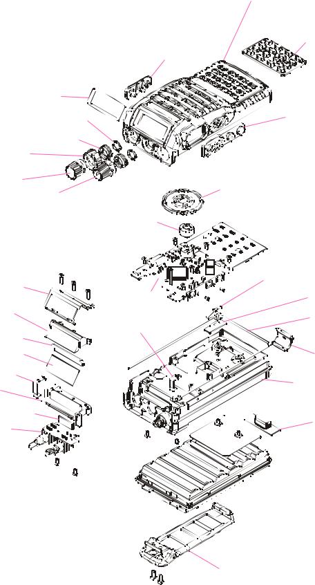
Exploded View & Miscellaneous Parts |
||
REF. |
VXSTD P/N |
Description |
Qty. |
|
|
c |
U07230102 |
PAN HEAD SCREW M2×3NI #1 |
1 |
|
|
d |
U9900101 |
PAN HEAD SCREW M1.7×14NI #2 |
1 |
|
|
e |
U9900098 |
TAPTITE SCREW M2×7NI #3 |
3 |
CP9485001 |
|
f |
U9900063 |
TAPTITE SCREW M2×3.3Ni |
2 |
||
FRONT CASE ASS'Y |
|||||
g |
U9900068 |
TAPTITE SCREW M2×4Ni #3 |
9 |
||
|
|||||
h |
U9900086 |
TAPTITE SCREW M1.7×2.5B |
2 |
|
|
i |
U02206007 |
SEMS SCREW SM2.6x6B |
2 |
|
|
Non-designated parts are available only as part of a designated assembly.
RA1111800
WINDOW
|
RA1128200 |
RA0211500 |
RUBBER KNOB |
RUBBER CAP |
|
RA0111400 |
RA0210300 |
|
RUBBER KNOB |
||
RING NUT |
||
|
||
RA0210600 |
|
|
RUBBER PACKING |
|
|
RA1112100 |
|
|
KNOB |
|
|
RA1111900 |
M4090198 |
|
VOLUME KNOB |
||
RA1112000 |
SPEAKER |
|
ENCODER KNOB |
|
|
|
RA0110200 |
|
|
HOLDER RUBBER |
RA0210100 |
|
RA0210700 |
|
TERMINAL PLATE |
|
HOLDER |
MAIN Unit |
RA1063600 |
|
||
RA020950A |
|
SPACER |
LIGHT GUIDE |
RA010690A |
RA021020A |
|
RUBBER PACKING |
|
RA0211100 |
TERMINAL PLATE L |
|
INTER CONNECTOR |
|
|
G6090137 |
|
RA055770C |
LCD |
|
LATCH NAIL |
RA010700A |
|
|
TERMINAL PLATE R |
|
CP9482001 |
RA0209600 |
|
|
|
REAR CASE ASSY |
|
BRACKET |
|
|
RA0211200 |
|
|
INTER CONNECTOR |
|
DUMMY Unit |
VR Unit |
|
|
|
|
CP9486001
BELT CLIP ASS'Y
FT-250R Technical Supplement |
3 |
Exploded View & Miscellaneous Parts
Note
4 |
FT-250R Technical Supplement |

Block Diagram
FT-250R Technical Supplement |
5 |
Block Diagram
Note:
6 |
FT-250R Technical Supplement |
Receive Signal Path
Incoming RF from the antenna jack is delivered to the RF Unit and passes through a low-pass filter and high-pass filter consisting of coils L1001, L1002, L1003, L1004, L1014 & L1015, capacitors C1001, C1002, C1003, C1004, C1006, C1007, C1042, C1044, C1045, C1046 & C1047, and antenna switching diode D1001 (RLS135).
Signals within the frequency range of the transceiver are then amplified by Q1011 (2SC5006) and enter a varac- tor-tuned band-pass filter consisting of coils L1016, L1017 & L1018, capacitors C1049, C1050, C1051, C1052, C1053, C1054, C1056, C1057, C1058, C1059, C1060, C1061, C1062 & C1063, and diodes D1004, D1005 & D1006 (all HVC350B) before delivery to the first mixer, Q1013
(3SK296ZQ).
Buffered output from the VCO is amplified by Q1018 (2SC5374) to provide a pure first local signal between 122.3 and 126.3 MHz according to the transceiver version and the programmed receiving frequency for injection to the first mixer Q1013. The 21.7 MHz first mixer product then passes through monolithic crystal filter XF1001 (21R12A4, 6 kHz BW) to strip away unwanted mixer products, and the IF signal is then amplified by Q1014
(2SC4400).
The amplified first IF signal is applied to FM IF subsystem IC Q1017 (TA31136FN), which contains the second mixer, limiter amplifier, noise amplifier, and S-meter amplifier.
A second local signal is generated by the reference oscillator section of the PLL subsystem IC Q1030 (MB15A01PFV1) using 21.25 MHz crystal X1001; a 450 kHz second IF is produced when this signal is mixed with the first IF signal within Q1017.
The second IF then passes through the main selectivity element, ceramic filter CF1001 (CFWM450E) to strip away all but the desired signal; it is then applied to the limiter amplifier in Q1017, which removes amplitude variations in the 450kHz IF, before detection of the speech by the ceramic discriminator CD1001 (JTBM450CX24).
Detected audio from Q1017 is applied to a low-pass filter consisting of capacitors C1208, C1209 & C1210, resistors R1320, R1321, R1322, R1323 & R1324, and Q1060 (NJM2902V), then passes through the audio mute gate Q1044 and Q1063 (both 2SC4081) to the buffer amplifier Q1043 (2SC4617); it is then passed through the deemphasis network consisting of capacitor C1057 and resistor R1208 to a high-pass filter consisting of capacitors C1058, C1059 & C1060, resistors R1209 & R1210, and
Q1064 (NJM2902V).
Circuit Description
The processed audio passes through the another audio mute gate Q1041 and Q1042 (both 2SC4081) to the volume control potentiometer VR3001 on the VR Unit, then is delivered to the audio amplifier Q1053 (DTA2822L), which provides up to 0.5 Watt to the headphone jack or an 8-W loudspeaker.
Squelch Control
The squelch circuitry consists of a noise amplifier, bandpass filter, noise detector & noise comparator within
Q1017, audio control gate Q1041, Q1042, Q1044, Q1063
(all 2SC4081), microprocessor Q1035 (M3826AEFGP), and squelch controller S3001 on the VR Unit.
When no carrier received, noise at the output of the detector stage in Q1017 is amplified and band-pass filtered by the noise amplifier section of Q1017 and the network between pins 7 and 8, and then rectified by the noise detector section of Q1017. The resulting DC squelch control voltage outputs at pin 13 of Q1017, then it is passed to pin 4 of the microprocessor Q1035.
If no carrier is received, this signal causes pins 44 and 47 of Q1035 to go “Low” and pin 54 to go “High.” Pin 47 disables the supply voltage to the audio amplifier Q1053 (TDA2822L), and pin 54 activates the audio control gates Q1041, Q1042, Q1044, Q1063, Q1049 and Q1050. Thus, the microprocessor Q1035 blocks output from the audio amplifier, and silences the receiver, while no signal is being received (and during transmission, as well). Meanwhile, pin 44 signals Q1056 (2SC4081) to hold the green (Busy) half of the LED D3001 (BRPY1211F) on the VR Unit off.
When a carrier appears at the discriminator, noise is removed from the output, causing pin 4 of Q1035 to go “low” and the microprocessor to activate the audio amplifier, audio mute gate, and “Busy” LED.
The microprocessor then checks for CTCSS or CDCSS code squelch information, if enabled, or for DTMF data on the optional DTMF Unit. If not transmitting and CTCSS or CDCSS is not activated, or if the received tone or code matches that programmed, the microprocessor stops scanning (if active) and allows audio to pass through the audio amplifier Q1053 to the loudspeaker by enabling the supply voltage to it via Q1047 (2SB1132Q), Q1048
(UMW1).
FT-250R Technical Supplement |
7 |
Circuit Description
Transmit Signal Path
Speech input from the microphone is amplified by Q1064 (NJM2902V), then filtered and sent to any installed optional signaling unit. The audio which returns from the optional unit then is passed to the pre-emphasis network.
The processed audio may then be mixed with a CTCSS tone generated by the microprocessor Q1035 (M3826AEFGP); it is then delivered to D1010 (HSC277) for frequency modulation of the PLL carrier (up to ±5kHz from the unmodulated carrier) at the transmitting frequency.
If an external microphone is used, PTT switching is controlled by Q1054 (UMZ2N), which signals the microprocessor Q1035 when the impedance at the microphone jack drops.
If a CDCSS code is enabled for transmission, the code is generated by microprocessor Q1035 and delivered to D1015 (HVC350B) for CDCSS modulating.
If DTMF is enabled for transmission, the tone is generated by the microprocessor Q1035 and applied to the splatter filter section in place of the speech audio. Also, the tone is amplified for monitoring in the loudspeaker.
The modulated signal from the VCO Q1023 (2SC5374) is buffered by Q1022 and Q1018 (both 2SC5374). The lowlevel transmit signal is amplified by Q1010 (2SC5226-5) and Q1009 (2SK3074); it is then applied to the final amplifier Q1008 (RD07MVS1A), which provides up to 5 watts output power.
The transmit signal then passes through the antenna switch D1001 (RLS135) and is low-pass filtered to suppress harmonic spurious radiation before delivery to the antenna.
Automatic Transmit Power Control
Drain current of the final amplifier Q1008 (RD07MVS1A) is sampled by R1028 and R1035. The resulting DC is fed back through the APC amplifier Q1003 (NJM2904V) to the driver amplifier Q1009 (2SK3074) and final amplifier Q1008, for control of the power output.
The microprocessor selects either “High” or “Low” power levels.
Transmit Inhibit
When the PLL is unlocked, pin 7 of PLL subsystem IC Q1030 (MB15A01PFV1) goes to a logic “Low.” The resulting DC unlock control voltage is passed through the inversion amplifier Q1032 (2SA1774) to pin 8 of the microprocessor Q1035. While the PLL is unlocked, pin 15 of Q1035 remains “Low,” disabling the gate voltages of driver amplifier Q1009 (2SK3074) and final amplifier Q1008 (RD07MVS1A), thereby disabling the transmitter.
Spurious Suppression
Generation of spurious products by the transmitter is minimized by the fundamental carrier frequency being equal to final transmitting frequency, modulated directly in the transmit VCO. Additional harmonic suppression is provided by a low-pass filter consisting of coils L1001, L1002, L1003, L1006, L1007 & L1008 and capacitors C1001, C1002, C1003, C1004, C1006, C1007, C1019, C1020, C1021 & C1022, resulting in more than 60 dB of harmonic suppression prior to delivery to the antenna.
PLL Frequency Synthesizer
The PLL circuitry on the Main Unit consists of VCO Q1023 (2SC5374), VCO buffers Q1022 and Q1019 (both 2 S C 5 3 7 4 ) , a n d P L L s u b s y s t e m I C Q 1 0 3 0 (MB15A01PFV1), which contains a reference divider, se- rial-to-parallel data latch, programmable divider, phase comparator, and charge pump.
Stability is maintained by a regulated 3.3 V supply provided via Q1051 (S-812C33AUA) and 21.25 MHz reference frequency crystal X1001, as well as the reference oscillator’s temperature compensating thermistor and capacitors.
While receiving, VCO Q1023 oscillates between 122.3 and 126.3 MHz according to the transceiver version and the programmed receiving frequency. The VCO output is buffered by Q1022 and Q1019, then applied to the prescaler section of Q1030. There the VCO signal is divided by 64 or 65, according to a control signal from the data latch section of Q1030, before being sent to the programmable divider section of Q1030.
The data latch section of Q1030 also receives serial dividing data from the microprocessor, Q1035, which causes the pre-divided VCO signal to be further divided in the programmable divider section, depending upon the desired receive frequency, so as to produce a 5 kHz or 6.25 kHz derivative of the current VCO frequency.
Meanwhile, the reference divider section of Q1030 divides the 21.25 MHz crystal reference X1001, by 4250 (or 3400) to produce the 5 kHz (or 6.25 kHz) loop reference (respectively).
The 5 kHz (or 6.25 kHz) signal from the programmable divider (derived from the VCO) and that derived from the reference oscillator are applied to the phase detector section of Q1030, which produces a pulsed output with pulse duration depending on the phase difference between the input signals.
8 |
FT-250R Technical Supplement |
Circuit Description
This pulse train is filtered to DC and returned to the varactor D1011 (HVC350B). Changes in the level of the DC voltage applied to the varactor affect the reference in the tank circuit of the VCO according to the phase difference between the signals derived from the VCO and the crystal reference oscillator.
The VCO is thus phase-locked to the crystal reference oscillator. The output of the VCO Q1023, after buffering by Q1022 and amplification by Q1018, is applied to the first mixer as described previously.
For transmission, the VCO Q1023 oscillates between 144 and 148 MHz according to the model version and programmed transmit frequency. The remainder of the PLL circuitry is shared with the receiver. However, the dividing data from the microprocessor is such that the VCO frequency is at the actual transmit frequency (rather than offset for IFs, as in the receiving case). Also, the VCO is modulated by the speech audio applied to D1010 (HSC277), as described previously.
Receive and transmit buses select which VCO is made active by Q1020 (DTA144TE). When the power saving feature is active, the microprocessor Q1035 (M3826AEFGP) periodically signals switches the Q1033 (DTA114TE) and Q1034 (2SC4081) for the PLL subsystem IC Q1030 to conserve power and shortens the lock-up time.
Miscellaneous Circuits
Push-To-Talk Transmit Activation
The PTT switch is connected to pin 28 of microprocessor Q1035 (M3826AEFGP), so that when the PTT switch is closed, pin 6 of Q1035 goes “High.” This signals the microprocessor to activate the TX/RX controller Q1028 (UMW1), which then disables the receiver by disabling the 5 V supply bus at Q1026 (DTA143XE) to the frontend, FM IF subsystem IC Q1017 (TA31136FN).
At the same time, Q1027 (2SA1586Y) activates the transmit 5V supply line to enable the transmitter.
FT-250R Technical Supplement |
9 |
Alignment
Introduction
The FT-250R is carefully aligned at the factory for the specified performance across the amateur band. Realignment should therefore not be necessary except in the event of a component failure. Only an authorized Vertex Standard representative should perform all component replacement and service, or the warranty policy may be void.
The following procedures cover the adjustments that are not normally required once the transceiver has left the factory. However, if damage occurs and some parts subsequently are replaced, realignment may be required. If a sudden problem occurs during normal operation, it is likely due to component failure; realignment should not be done until after the faulty component has been replaced.
We recommend that servicing be performed only by authorized Vertex Standard service technicians who are experienced with the circuitry and fully equipped for repair and alignment. If a fault is suspected, contact the dealer from whom the transceiver was purchased for instructions regarding repair. Authorized Vertex Standard service technicians realign all circuits and make complete performance checks to ensure compliance with factory specifications after replacing any faulty components.
Those who do undertake any of the following alignments are cautioned to proceed at their own risk. Problems caused by unauthorized attempts at realignment are not covered by the warranty policy. Also, Vertex Standard reserves the right to change circuits and alignment procedures in the interest of improved performance, without notifying owners.
Under no circumstances should any alignment be attempted unless the normal function and operation of the transceiver are clearly understood, the cause of the malfunction has been clearly pinpointed and any faulty components replaced, and realignment determined to be absolutely necessary.
Required Test Equipment
The following test equipment (and familiarity with its use) is necessary for complete realignment. Correction of problems caused by misalignment resulting from use of improper test equipment is not covered under the warranty policy. While most steps do not require all of the equipment listed, the interactions of some adjustments may require that more complex adjustments be performed afterwards.
Do not attempt to perform only a single step unless it is clearly isolated electrically from all other steps. Have all test equipment ready before beginning and, follow all of the steps in a section in the order presented.
RF Signal Generator with calibrated output level at 200 MHz
Deviation Meter (linear detector)
In-line Wattmeter with 5% accuracy at 200 MHz
50-Ohm 10-W RF Dummy Load
8-Ohm AF Dummy Load
Regulated DC Power Supply adjustable from 3 to 16.5 VDC, 2A
Frequency Counter: 0.2-ppm accuracy at 200 MHz
AF Signal Generator
AC Voltmeter
DC Voltmeter: high impedance
VHF Sampling Coupler
SINAD Meter
Alignment Preparation & Precautions
A 50-Ohm RF load and in-line wattmeter must be connected to the main antenna jack in all procedures that call for transmission; alignment is not possible with an antenna. After completing one step, read the next step to see if the same test equipment is required. If not, remove the test equipment (except dummy load and wattmeter, if connected) before proceeding.
Correct alignment requires that the ambient temperature be the same as that of the transceiver and test equipment, and that this temperature be held constant between 68 ~ 86° F (20° ~ 30° C). When the transceiver is brought into the shop from hot or cold air, it should be allowed some time to come to room temperature before alignment. Whenever possible, alignments should be made with oscillator shields and circuit boards firmly affixed in place. Also, the test equipment must be thoroughly warmed up before beginning.
Note: Signal levels in dB referred to in the alignment procedure are based on 0dBµ = 0.5µV.
10 |
FT-250R Technical Supplement |
 Loading...