

Texas Instruments CD74HCT238M, CD74HCT238E, CD74HCT138M96, CD74HCT138M, CD74HCT138E Datasheet
...
CD74HC138, CD74HCT138,
/
j
[ /Title
(CD74
HC138
,
CD74
HCT13
8,
CD74
HC238
,
CD74
HCT23
8)
Subect
(High
Speed
Data sheet acquired from Harris Semiconductor
SCHS147A
October 1997 - Revised February 1999
Features
• Select One Of Eight Data Outputs
Active Low for 138, Active High for 238
• l/O Port or Memory Selector
• Three Enable Inputs to Simplify Cascading
• Typical Propagation Delay of 13ns at V
C
= 15pF, TA = 25oC
L
• Fanout (Over Temperature Range)
- Standard Outputs. . . . . . . . . . . . . . . 10 LSTTL Loads
- Bus Driver Outputs . . . . . . . . . . . . . 15 LSTTL Loads
• Wide Operating Temperature Range . . . -55
• Balanced Propagation Delay and Transition Times
• Significant Power Reduction Compared to LSTTL
Logic ICs
• HC Types
- 2V to 6V Operation
- High Noise Immunity: N
at VCC = 5V
• HCT Types
- 4.5V to 5.5V Operation
- Direct LSTTL Input Logic Compatibility,
V
= 0.8V (Max), VIH = 2V (Min)
IL
- CMOS Input Compatibility, I
= 30%, NIH = 30% of V
IL
≤ 1µA at VOL, V
l
CC
= 5V,
o
CD74HC238, CD74HCT238
High Speed CMOS Logic 3-to-8 Line Decoder/
Demultiplexer Inverting and Non-Inverting
C to 125oC
CC
OH
Pinout
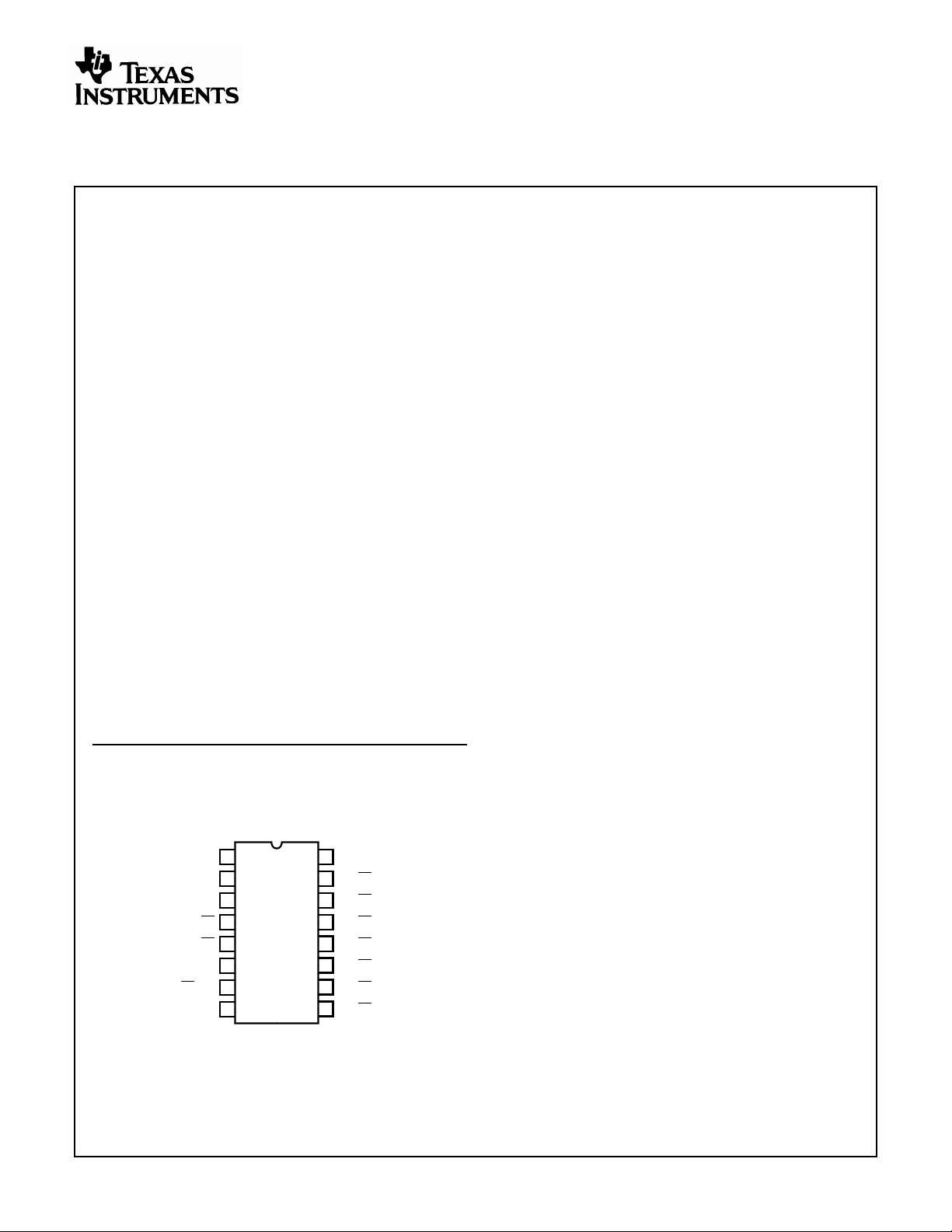
CD74HC138, CD74HCT138, CD74HC238, CD74HCT238
(PDIP, SOIC)
TOP VIEW
V
1
A0
A1
2
A2
3
4
E1
5
E2
E3
6
GND
7
8
(Y7) Y7
Signal names in parentheses are for ’HC238 and ’HCT238.
CAUTION: These devices are sensitive to electrostatic discharge. Users should follow proper IC Handling Procedures.
Copyright
© 1999, Texas Instruments Incorporated
16
15
14
13
12
11
10
9
CC
Y0)
Y0 (
Y1 (Y1)
Y2 (Y2)
Y3 (Y3)
Y4 (
Y4)
Y5)
Y5 (
Y6 (
Y6)
1
CD74HC138, CD74HCT138, CD74HC238, CD74HCT238
Description
The Harris CD74HC138, CD74HC238 and CD74HCT138,
CD74HCT238 are high speed silicon gate CMOS decoders
well suited to memory address decoding or data routing
applications. Both circuits feature low power consumption
usually associated with CMOS circuitry, yet have speeds
comparable to low power Schottky TTL logic. Both circuits
have three binary select inputs(A0, A1 and A2). If the device
is enabled, these inputs determine which one of the eight
normally high outputs of the HC/HCT138 series will go low
or which of the normally low outputs of the HC/HCT238
series will go high.
Two active low and one active high enables (
E1, E2, and E3)
are provided to ease the cascading of decoders. The
decoder’s 8 outputs can drive 10 low power Schottky TTL
equivalent loads.
Ordering Information
PKG.
PART NUMBER TEMP. RANGE (oC) PACKAGE
CD74HC138E -55 to 125 16 Ld PDIP E16.3
NO.
Ordering Information
PKG.
PART NUMBER TEMP. RANGE (oC) PACKAGE
CD74HCT138E -55 to 125 16 Ld PDIP E16.3
CD74HC238E -55 to 125 16 Ld PDIP E16.3
CD74HCT238E -55 to 125 16 Ld PDIP E16.3
CD74HC138M -55 to 125 16 Ld SOIC M16.15
CD74HCT138M -55 to 125 16 Ld SOIC M16.15
CD74HC238M -55 to 125 16 Ld SOIC M16.15
CD74HCT238M -55 to 125 16 Ld SOIC M16.15
CD74HC138SM -55 to 125 16 Ld SSOP M16.209
NOTES:
1. When ordering, use the entire partnumber. Add the suffix 96 to
obtain the variant in the tape and reel.
2. Wafer and die for this part number is available which meets all
electrical specifications. Please contact your local sales office or
Harris customer service for ordering information.
NO.
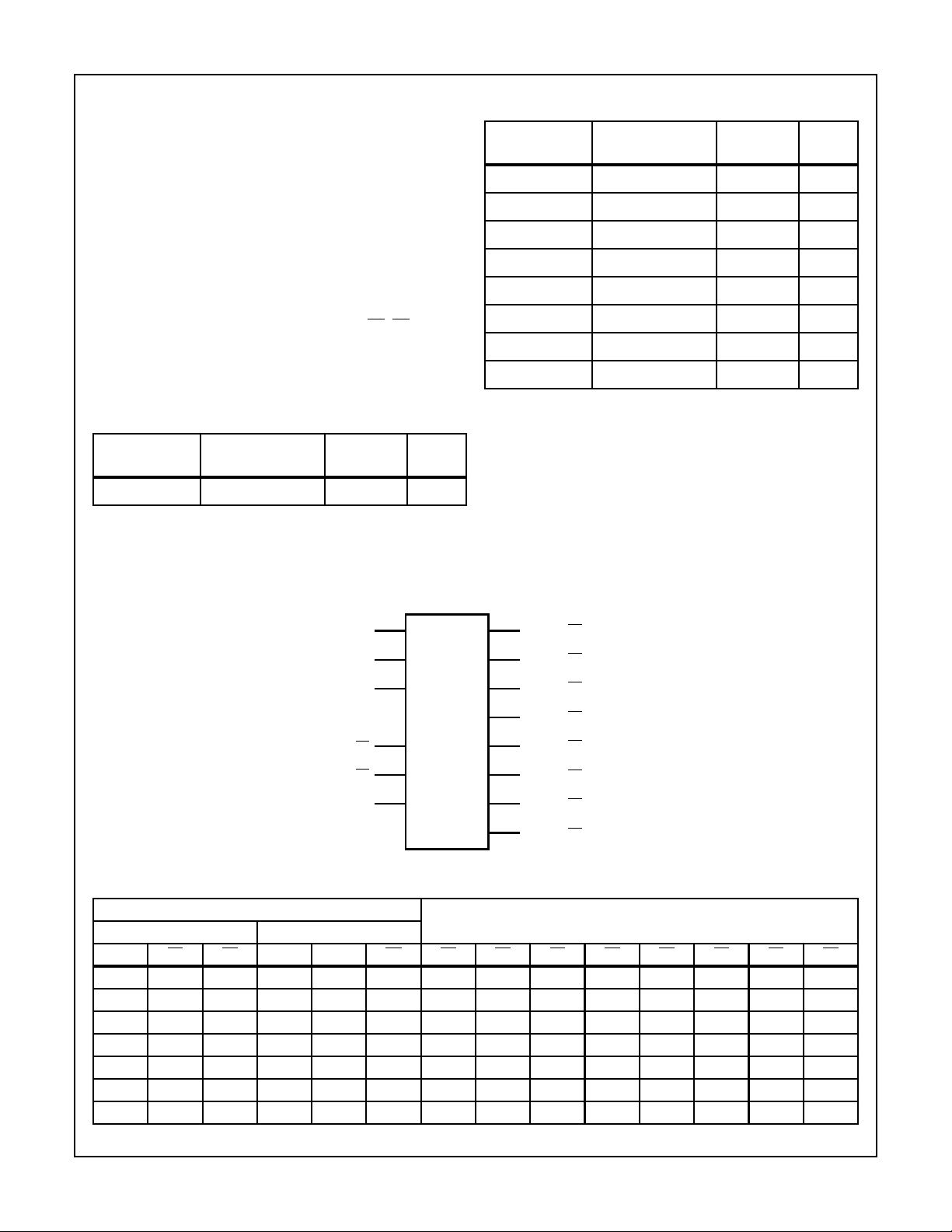
Functional Diagram
HC/HCT
HC/HCT
238
Y1
Y2
Y3
Y4
Y5
Y6
Y7
138
Y0
Y1
Y2
Y3
Y4
Y5
Y6
Y7
OUTPUTSENABLE ADDRESS
1
A0 Y0
2
A1
3
A2
4
E1
5
E2
6
E3
15
14
13
12
11
10
9
7
TRUTH TABLE CD74HC138, CD74HCT138
INPUTS
E3 E2 E1 A2 A1 A0 Y0 Y1 Y2 Y3 Y4 Y5 Y6 Y7
XXHXXXHHHHHHHH
LXXXXXHHHHHHHH
XHXXXXHHHHHHHH
HLLLLLLHHHHHHH
HLLLLHHLHHHHHH
HLLLHLHHLHHHHH
HL LLHHHHHLHHHH
2
CD74HC138, CD74HCT138, CD74HC238, CD74HCT238
TRUTH TABLE CD74HC138, CD74HCT138
INPUTS
OUTPUTSENABLE ADDRESS
E3
HLLHLLHHHHLHHH
HLLHLHHHHHHLHH
HLLHHLHHHHHHLH
HLLHHHHHHHHHHL
NOTE: H = High Voltage Level, L = Low Voltage Level, X = Don’t Care
E3
XXHXXXLLLLLLLL
LXXXXXLLLLLLLL
XHXXXXLLLLLLLL
HLLLLLHLLLLLLL
HLLLLHLHLLLLLL
HLLLHLLLHLLLLL
HLLLHHLLLHLLLL
HLLHLLLLLLHLLL
HLLHLHLLLLLHLL
HLLHHLLLLLLLHL
HLLHHHLLLLLLLH
NOTE: H = High Voltage Level, L = Low Voltage Level, X = Don’t Care
E2 E1 A2 A1 A0 Y0 Y1 Y2 Y3 Y4 Y5 Y6 Y7
TRUTH TABLE CD74HC238, CD74HCT238
INPUTS
OUTPUTSENABLE ADDRESS
E2 E1 A2 A1 A0 Y0 Y1 Y2 Y3 Y4 Y5 Y6 Y7
3
CD74HC138, CD74HCT138, CD74HC238, CD74HCT238
Absolute Maximum Ratings Thermal Information
DC Supply Voltage, VCC. . . . . . . . . . . . . . . . . . . . . . . . -0.5V to 7V
DC Input Diode Current, I
IK
For VI < -0.5V or VI > VCC + 0.5V. . . . . . . . . . . . . . . . . . . . . .±20mA
DC Output Diode Current, I
OK
For VO < -0.5V or VO > VCC + 0.5V . . . . . . . . . . . . . . . . . . . .±20mA
DC Output Source or Sink Current per Output Pin, I
O
For VO > -0.5V or VO < VCC + 0.5V . . . . . . . . . . . . . . . . . . . .±25mA
DC VCC or Ground Current, I
CC orIGND
. . . . . . . . . . . . . . . . . .±50mA
Operating Conditions
Temperature Range (TA) . . . . . . . . . . . . . . . . . . . . . -55oC to 125oC
Supply Voltage Range, V
HC Types . . . . . . . . . . . . . . . . . . . . . . . . . . . . . . . . . . . . .2V to 6V
HCT Types . . . . . . . . . . . . . . . . . . . . . . . . . . . . . . . . .4.5V to 5.5V
DC Input or Output Voltage, VI, VO . . . . . . . . . . . . . . . . . 0V to V
Input Rise and Fall Time
2V . . . . . . . . . . . . . . . . . . . . . . . . . . . . . . . . . . . . . . 1000ns (Max)
4.5V. . . . . . . . . . . . . . . . . . . . . . . . . . . . . . . . . . . . . . 500ns (Max)
6V . . . . . . . . . . . . . . . . . . . . . . . . . . . . . . . . . . . . . . . 400ns (Max)
CAUTION: Stresses above those listed in “Absolute Maximum Ratings” may cause permanent damage to the device. This is a stress only rating and operation
of the device at these or any other conditions above those indicated in the operational sections of this specification is not implied.
NOTE:
3. θJA is measured with the component mounted on an evaluation PC board in free air.
CC
Thermal Resistance (Typical, Note 3) θJA (oC/W)
PDIP Package. . . . . . . . . . . . . . . . . . . . . . . . . . . . . 90
SOIC Package. . . . . . . . . . . . . . . . . . . . . . . . . . . . . 115
SSOP Package . . . . . . . . . . . . . . . . . . . . . . . . . . . . 155
Maximum Junction Temperature. . . . . . . . . . . . . . . . . . . . . . .150oC
Maximum Storage Temperature Range . . . . . . . . . .-65oC to 150oC
Maximum Lead Temperature (Soldering 10s). . . . . . . . . . . . .300oC
(SOIC - Lead Tips Only)
CC
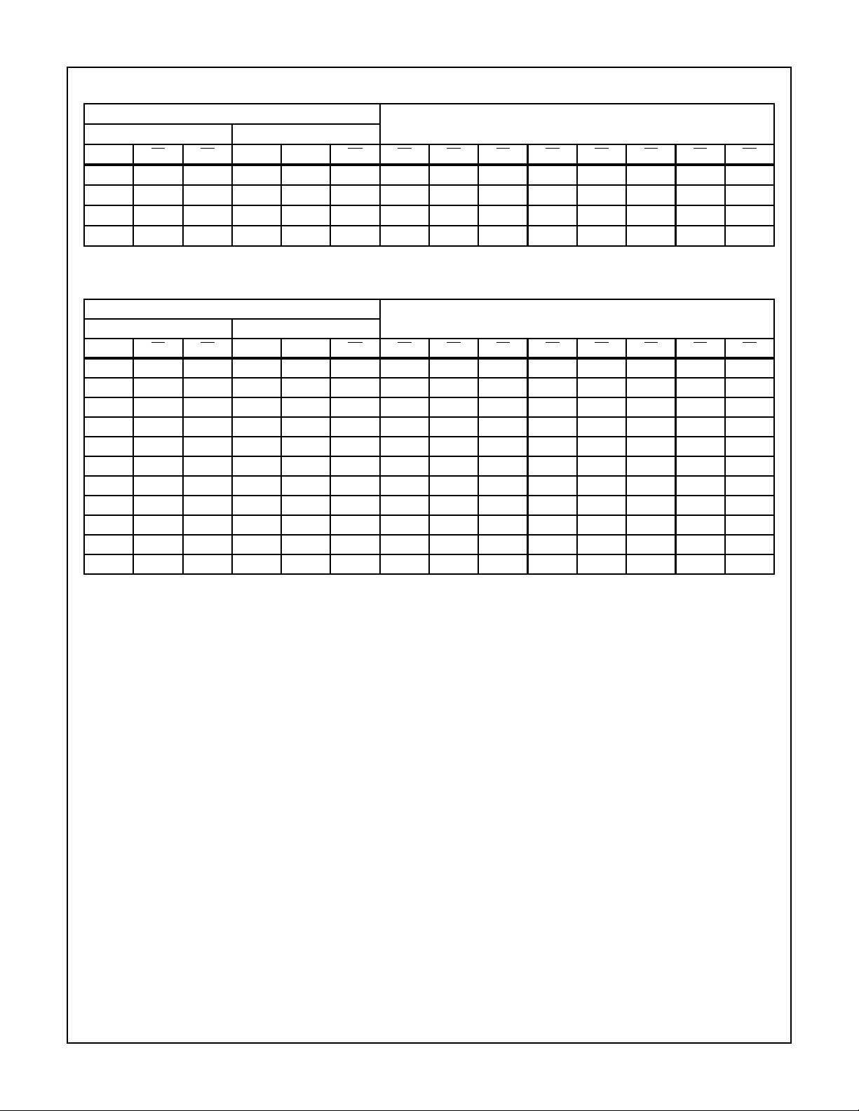
DC Electrical Specifications
PARAMETER SYMBOL
HC TYPES
High Level Input
Voltage
Low Level Input
Voltage
High Level Output
Voltage
CMOS Loads
High Level Output
Voltage
TTL Loads
Low Level Output
Voltage
CMOS Loads
Low Level Output
Voltage
TTL Loads
Input Leakage
Current
Quiescent Device
Current
V
IH
V
IL
V
OH
V
OL
I
I
I
CC
TEST
CONDITIONS
(V) IO(mA) MIN TYP MAX MIN MAX MIN MAX
I
V
CC
(V)
o
C -40oC TO 85oC -55oCTO125oC
25
UNITSV
- - 2 1.5 - - 1.5 - 1.5 - V
4.5 3.15 - - 3.15 - 3.15 - V
6 4.2 - - 4.2 - 4.2 - V
- - 2 - - 0.5 - 0.5 - 0.5 V
4.5 - - 1.35 - 1.35 - 1.35 V
6 - - 1.8 - 1.8 - 1.8 V
VIHor VIL-0.02 2 1.9 - - 1.9 - 1.9 - V
-0.02 4.5 4.4 - - 4.4 - 4.4 - V
-0.02 6 5.9 - - 5.9 - 5.9 - V
- - ---- - - - V
-4 4.5 3.98 - - 3.84 - 3.7 - V
-5.2 6 5.48 - - 5.34 - 5.2 - V
VIHor VIL0.02 2 - - 0.1 - 0.1 - 0.1 V
0.02 4.5 - - 0.1 - 0.1 - 0.1 V
0.02 6 - - 0.1 - 0.1 - 0.1 V
- - ---- - - - V
4 4.5 - - 0.26 - 0.33 - 0.4 V
5.2 6 - - 0.26 - 0.33 - 0.4 V
VCC or
-6--±0.1 - ±1-±1µA
GND
VCC or
0 6 - - 8 - 80 - 160 µA
GND
4

CD74HC138, CD74HCT138, CD74HC238, CD74HCT238
DC Electrical Specifications (Continued)
TEST
CONDITIONS
PARAMETER SYMBOL
HCT TYPES
High Level Input
Voltage
Low Level Input
Voltage
High Level Output
Voltage
V
IH
V
IL
V
OH
CMOS Loads
High Level Output
Voltage
TTL Loads
Low Level Output
Voltage
V
OL
CMOS Loads
Low Level Output
Voltage
TTL Loads
Input Leakage
Current
Quiescent Device
Current
Additional Quiescent
Device Current Per
I
I
I
CC
∆I
CC
Input Pin: 1 Unit Load
(Note 4)
NOTE:
4. For dual-supply systems theoretical worst case (V
(V) IO(mA) MIN TYP MAX MIN MAX MIN MAX
I
- - 4.5 to
- - 4.5 to
VIHor VIL-0.02 4.5 4.4 - - 4.4 - 4.4 - V
VIHor VIL0.02 4.5 - - 0.1 - 0.1 - 0.1 V
VCCand
GND
VCC or
GND
V
CC
-2.1
o
C -40oC TO 85oC -55oCTO125oC
V
CC
(V)
25
UNITSV
2--2- 2 - V
5.5
- - 0.8 - 0.8 - 0.8 V
5.5
-4 4.5 3.98 - - 3.84 - 3.7 - V
4 4.5 - - 0.26 - 0.33 - 0.4 V
0 5.5 - ±0.1 - ±1-±1µA
0 5.5 - - 8 - 80 - 160 µA
- 4.5 to
- 100 360 - 450 - 490 µA
5.5
= 2.4V, VCC = 5.5V) specification is 1.8mA.
I
HCT Input Loading Table
INPUT UNIT LOADS
A0-A2 1.5
E1, E2 1.25
E3 1
NOTE: Unit Load is ∆ICClimit specified in DC Electrical Table, e.g.,
360µA max at 25oC.
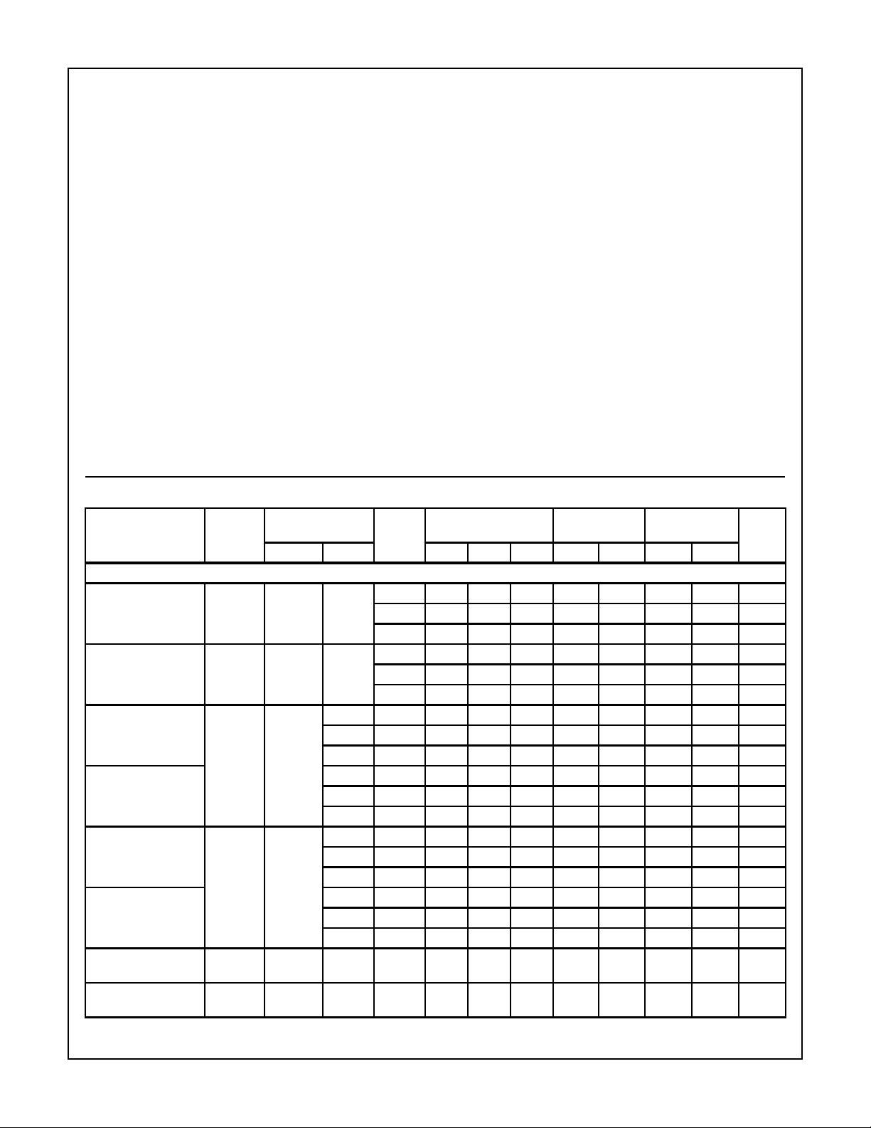
Switching Specifications Input t
PARAMETER SYMBOL
HC TYPES
Propagation Delay t
Address to Output 4.5 - - 30 - 38 - 45 ns
, tf = 6ns
r
CONDITIONS V
PLH,tPHLCL
CL= 15pF 5 - 13 - - - - - ns
C
-40oC TO
85oC -55oC TO 125oC
TEST
CC
(V)
25
o
C
= 50pF 2 - - 150 - 190 - 225 ns
= 50pF 6 - - 26 - 33 - 38 ns
L
UNITSMIN TYP MAX MIN MAX MIN MAX
5

Switching Specifications Input t
PARAMETER SYMBOL
Enable to Output
HC/HCT138
Output Transition Time
(Figure 1)
Power Dissipation
Capacitance, (Notes 5, 6)
Input Capacitance C
HCT TYPES
Propagation Delay
Address to Output t
Enable to Output
HC/HCT138
Enable to Output
HC/HCT238
Output Transition Time
(Figure 2)
Power Dissipation
Capacitance, (Notes 5, 6)
Input Capacitance C
NOTES:
5. C
is used to determine the dynamic power consumption, per gate.
PD
6. PD = V
2
fi(CPD + CL) where: fi = Input Frequency, CL = Output Load Capacitance, VCC = Supply Voltage.
CC
t
PLH,tPHLCL
t
TLH
C
PLH
t
PLH
t
PLH,tPHLCL
t
TLH
C
, tf = 6ns (Continued)
r
-40oC TO
85oC -55oC TO 125oC
TEST
25
o
C
CONDITIONS VCC(V)
= 50pF 2 - - 150 - 190 - 265 ns
4.5 - - 30 - 38 - 53 ns
6 - - 26 - 33 - 45 ns
, t
THLCL
= 50pF 2 - - 75 - 95 - 110 ns
4.5 - - 15 - 19 - 22 ns
6 - - 13 - 16 - 19 ns
CL= 15pF 5 - 67 - - - - - pF
PD
IN
, t
PHLCL
, t
PHLCL
- - - - 10 - 10 - 10 pF
= 50pF 4.5 - - 35 - 44 - 53 ns
C
= 15pF 5 - 14 - - - - - ns
L
= 50pF 4.5 - - 35 - 44 - 53 ns
= 15pF 4.5 - - 40 - 50 - 60 ns
, t
THLCL
PD
IN
= 50pF 4.5 - - 15 - 19 - 22 ns
CL= 15pF 5 - 67 - - - - - pF
- - - - 10 - 10 - 10 pF
UNITSMIN TYP MAX MIN MAX MIN MAX
Test Circuits and Waveforms
tr = 6ns tf = 6ns
V
t
TLH
CC
GND
t
PHL
90%
50%
10%
t
90%
50%
10%
PLH
INPUT
t
INVERTING
OUTPUT
THL
FIGURE 7. HC AND HCU TRANSITION TIMES AND PROPAGA-
TION DELAY TIMES, COMBINATION LOGIC
= 6ns
t
PLH
t
f
1.3V
10%
t
90%
TLH
tr = 6ns
INPUT
t
INVERTING
OUTPUT
THL
t
2.7V
1.3V
0.3V
PHL
FIGURE 8. HCT TRANSITION TIMES AND PROPAGATION
DELAY TIMES, COMBINATION LOGIC
6
3V
GND

IMPORTANT NOTICE
T exas Instruments and its subsidiaries (TI) reserve the right to make changes to their products or to discontinue
any product or service without notice, and advise customers to obtain the latest version of relevant information
to verify, before placing orders, that information being relied on is current and complete. All products are sold
subject to the terms and conditions of sale supplied at the time of order acknowledgement, including those
pertaining to warranty, patent infringement, and limitation of liability.
TI warrants performance of its semiconductor products to the specifications applicable at the time of sale in
accordance with TI’s standard warranty. Testing and other quality control techniques are utilized to the extent
TI deems necessary to support this warranty . Specific testing of all parameters of each device is not necessarily
performed, except those mandated by government requirements.
CERT AIN APPLICATIONS USING SEMICONDUCT OR PRODUCTS MAY INVOLVE POTENTIAL RISKS OF
DEATH, PERSONAL INJURY, OR SEVERE PROPERTY OR ENVIRONMENTAL DAMAGE (“CRITICAL
APPLICATIONS”). TI SEMICONDUCTOR PRODUCTS ARE NOT DESIGNED, AUTHORIZED, OR
WARRANTED TO BE SUITABLE FOR USE IN LIFE-SUPPORT DEVICES OR SYSTEMS OR OTHER
CRITICAL APPLICA TIONS. INCLUSION OF TI PRODUCTS IN SUCH APPLICATIONS IS UNDERST OOD TO
BE FULLY AT THE CUSTOMER’S RISK.
In order to minimize risks associated with the customer’s applications, adequate design and operating
safeguards must be provided by the customer to minimize inherent or procedural hazards.
TI assumes no liability for applications assistance or customer product design. TI does not warrant or represent
that any license, either express or implied, is granted under any patent right, copyright, mask work right, or other
intellectual property right of TI covering or relating to any combination, machine, or process in which such
semiconductor products or services might be or are used. TI’s publication of information regarding any third
party’s products or services does not constitute TI’s approval, warranty or endorsement thereof.
Copyright 1999, Texas Instruments Incorporated
 Loading...